
THS6052, THS6053
175 mA,
▒
12 V ADSL CPE LINE DRIVERS
SLOS293D ¡ JUNE 2000 ¡ REVISED DECEMBER 2001
1
POST OFFICE BOX 655303
À
DALLAS, TEXAS 75265
D
Remote Terminal ADSL Line Driver
¡ Ideal for Both Full Rate ADSL and G.Lite
¡ Compatible With 1:1 Transformer Ratio
D
Low 2.7 pA/
Hz Noninverting Current Noise
¡ Reduces Noise Feedback Through
Hybrid Into Downstream Channel
D
Wide Supply Voltage Range
▒
5 V to
▒
15 V
¡ Ideal for
▒
12-V Operation
D
Wide Output Swing
¡ 42 Vpp Differential Output Voltage,
R
L
= 200
,
▒
12-V Supply
D
High Output Current
¡ 175 mA (typ)
D
High Speed
¡ 110 MHz (¡3 dB, G=8,
▒
12 V)
¡ 1500 V/
Á
s Slew Rate (G = 8,
▒
12 V)
D
Low Distortion, Single-Ended, G = 8
¡ ¡83 dBc (250 kHz, 2 Vpp, 100-
load)
D
Low Power Shutdown (THS6053)
¡ 300-
Á
A Total Standby Current
D
Thermal Shutdown and Short Circuit
Protection
D
Standard SOIC, SOIC PowerPAD, and
TSSOP PowerPAD
Package
D
Evaluation Module Available
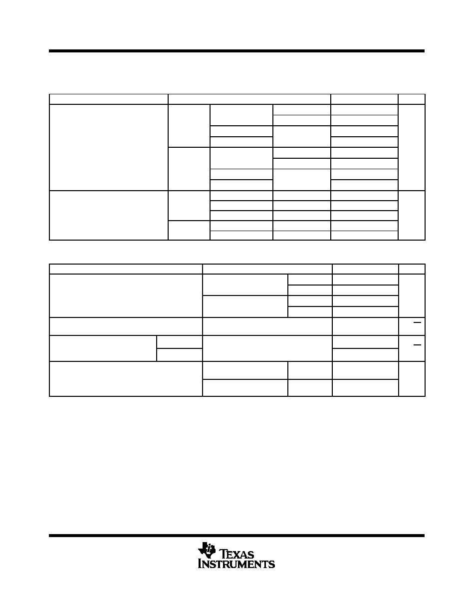
1
2
3
4
8
7
6
5
D1 OUT
D1 IN¡
D1 IN+
V
CC¡
V
CC+
D2 OUT
D2 IN¡
D2 IN+
THS6052
SOIC (D) AND
SOIC PowerPAD
(DDA) PACKAGE
(TOP VIEW)
1
2
3
4
5
6
7
14
13
12
11
10
9
8
D1 OUT
D1 IN¡
D1 IN+
V
CC¡
N/C
GND
N/C
V
CC+
D2 OUT
D2 IN¡
D2 IN+
N/C
SHUTDOWN
N/C
THS6053
SOIC (D) AND
TSSOP PowerPAD
(PWP) PACKAGE
(TOP VIEW)
description
The THS6052/3 is a high-speed line driver ideal for driving signals from the remote terminal to the central office
in asymmetrical digital subscriber line (ADSL) applications. It can operate from
▒
12-V supply voltages while
drawing only 5.2 mA of supply current per channel. It offers low ¡83 dBc total harmonic distortion driving a 100-
load (2 Vpp). The THS6052/3 offers a high 42-Vpp differential output swing across a 200-
load from a
▒
12-V
supply. The THS6053 features a low-power shutdown mode, consuming only 300
Á
A quiescent current per
channel. The THS6052/3 is packaged in a standard SOIC, SOIC PowerPAD
, and TSSOP PowerPAD
packages.
_
+
+12 V
750
VI+
_
+
¡12 V
750
VI¡
50
1:1
15.4 dBm
Delivered
to Telephone
Line
50
THS6052
Driver 1
THS6052
Driver 2
100
210
0.68
Á
F
RELATED PRODUCTS
DEVICE
THS6042/3
THS6092/3
OPA2677
THS6062
DESCRIPTION
350-mA,
▒
12 ADSL CPE line driver
275-mA, +12 V ADSL CPE line driver
380-mA, +12 V ADSL CPE line driver
Low noise ADSL receiver
Copyright
2001, Texas Instruments Incorporated
PRODUCTION DATA information is current as of publication date.
Products conform to specifications per the terms of Texas Instruments
standard warranty. Production processing does not necessarily include
testing of all parameters.
Please be aware that an important notice concerning availability, standard warranty, and use in critical applications of
Texas Instruments semiconductor products and disclaimers thereto appears at the end of this data sheet.
PowerPAD is a trademark of Texas Instruments.

THS6052, THS6053
175 mA,
▒
12 V ADSL CPE LINE DRIVERS
SLOS293D ¡ JUNE 2000 ¡ REVISED DECEMBER 2001
2
POST OFFICE BOX 655303
À
DALLAS, TEXAS 75265
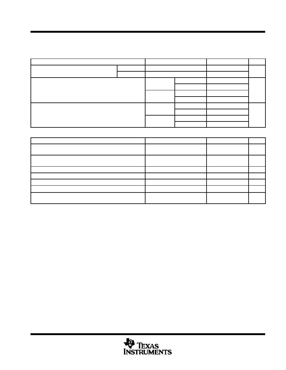
AVAILABLE OPTION
PACKAGED DEVICE
EVALUATION
TA
SOIC-8
(D)
SOIC-8 PowerPAD
(DDA)
SOIC-14
(D)
TSSOP-14
(PWP)
EVALUATION
MODULES
0
░
C to 70
░
C
THS6052CD
THS6052CDDA
THS6053CD
THS6053CPWP
THS6052EVM
THS6053EVM
¡ 40
░
C to 85
░
C
THS6052ID
THS6052IDDA
THS6053ID
THS6053IPWP
--
absolute maximum ratings over operating free-air temperature (unless otherwise noted)
Supply voltage, V
CC+
to V
CC¡
33
V
. . . . . . . . . . . . . . . . . . . . . . . . . . . . . . . . . . . . . . . . . . . . . . . . . . . . . . . . . . . . . . .
Input voltage
▒
V
CC
. . . . . . . . . . . . . . . . . . . . . . . . . . . . . . . . . . . . . . . . . . . . . . . . . . . . . . . . . . . . . . . . . . . . . . . . . . . .
Output current (see Note 1)
275 mA
. . . . . . . . . . . . . . . . . . . . . . . . . . . . . . . . . . . . . . . . . . . . . . . . . . . . . . . . . . . . . .
Differential input voltage
▒
4 V
. . . . . . . . . . . . . . . . . . . . . . . . . . . . . . . . . . . . . . . . . . . . . . . . . . . . . . . . . . . . . . . . . . .
Maximum junction temperature
150
░
C
. . . . . . . . . . . . . . . . . . . . . . . . . . . . . . . . . . . . . . . . . . . . . . . . . . . . . . . . . . . .
Total power dissipation at (or below) 25
░
C free-air temperature
See Dissipation Ratings Table
. . . . . . . . . . .
Operating free-air temperature, T
A
: Commercial 0
░
C to 70
░
C
. . . . . . . . . . . . . . . . . . . . . . . . . . . . . . . . . . . . . . . .
Industrial
¡ 40
░
C to 85
░
C
. . . . . . . . . . . . . . . . . . . . . . . . . . . . . . . . . . . . . . . .
Storage temperature, T
stg
: Commercial
¡ 65
░
C to 125
░
C
. . . . . . . . . . . . . . . . . . . . . . . . . . . . . . . . . . . . . . . . . . . .
Industrial
¡ 65
░
C to 125
░
C
. . . . . . . . . . . . . . . . . . . . . . . . . . . . . . . . . . . . . . . . . . . . . .
Lead temperature 1,6 mm (1/16 inch) from case for 10 seconds
300
░
C
. . . . . . . . . . . . . . . . . . . . . . . . . . . . . . .
Stresses beyond those listed under "absolute maximum ratings" may cause permanent damage to the device. These are stress ratings only, and
functional operation of the device at these or any other conditions beyond those indicated under "recommended operating conditions" is not
implied. Exposure to absolute-maximum-rated conditions for extended periods may affect device reliability.
NOTE 1: The THS6052 and THS6053 may incorporate a PowerPAD
on the underside of the chip. This acts as a heatsink and must be
connected to a thermally dissipating plane for proper power dissipation. Failure to do so may result in exceeding the maximum junction
temperature which could permanently damage the device. See TI technical brief SLMA002 for more information about utilizing the
PowerPAD
thermally enhanced package.
DISSIPATION RATING TABLE
PACKAGE
JA
JC
TA = 25
░
C
TJ = 150
░
C
POWER RATING
D-8
95
░
C/W
38.3
░
C/W
1.32 W
DDA
45.8
░
C/W
9.2
░
C/W
2.73 W
D-14
66.6
░
C/W
26.9
░
C/W
1.88 W
PWP
37.5
░
C/W
1.4
░
C/W
3.3 W
This data was taken using the JEDEC proposed high-K test PCB. For the JEDEC low-K test
PCB, the
JA is168
░
C/W for the D¡8 package and 122.3
░
C/W for the D¡14 package.
recommended operating conditions
MIN
NOM
MAX
UNIT
Supply voltage V
to V
Dual supply
▒
5
▒
15
V
Supply voltage, VCC+ to VCC¡
Single supply
10
30
V
Operating free air temperature T
C-suffix
0
70
░
C
Operating free-air temperature, TA
I-suffix
¡40
85
░
C
THS6052, THS6053
175 mA,
▒
12 V ADSL CPE LINE DRIVERS
SLOS293D ¡ JUNE 2000 ¡ REVISED DECEMBER 2001
3
POST OFFICE BOX 655303
À
DALLAS, TEXAS 75265
electrical characteristics over recommended operating free-air temperature range, T
A
= 25
░
C,
V
CC
=
▒
12 V, R
FEEDBACK
= 750
, R
L
= 100
(unless otherwise noted)
dynamic performance
PARAMETER
TEST CONDITIONS
MIN
TYP
MAX
UNIT
G= 1 RF = 1 k
VCC =
▒
5 V
110
RL = 50
G= 1, RF = 1 k
VCC =
▒
12 V
120
RL = 50
G= 2, RF = 680
VCC =
▒
5 V
▒
12 V
100
BW
Small signal bandwidth ( 3 dB)
G= 8, RF = 330
VCC =
▒
5 V,
▒
12 V
90
MHz
BW
Small-signal bandwidth (¡ 3 dB)
G= 1 RF = 1 k
VCC =
▒
5 V
150
MHz
RL = 100
G= 1, RF = 1 k
VCC =
▒
12 V
170
RL = 100
G= 2, RF = 680
VCC =
▒
5 V
▒
12 V
135
G= 8, RF = 330
VCC =
▒
5 V,
▒
12 V
110
VCC =
▒
5 V
VCC =
▒
5 V
650
VO = 4 VPP VCC =
▒
12 V
VCC =
▒
12 V
850
SR
Slew rate (see Note 2), G=8
VO 4 VPP
VCC =
▒
15 V
VCC =
▒
15 V
950
V/
Á
s
SR
Slew rate (see Note 2), G 8
V
16 V
VCC =
▒
12 V
VCC =
▒
12 V
1500
V/
Á
s
VO = 16 VPP
VCC =
▒
15 V
VCC =
▒
15 V
1700
NOTE 2: Slew rate is defined from the 25% to the 75% output levels.
noise/distortion performance
PARAMETER
TEST CONDITIONS
MIN
TYP
MAX
UNIT
Gain = 8,
RL = 100
,
VO(pp) = 2 V
¡ 83
THD
Total harmonic distortion (single-ended
Gain 8,
RL 100
,
VCC =
▒
12 V, f = 250 kHz
VO(pp) = 16 V
¡ 78
dBc
THD
Total harmonic distortion (single ended
configuration)
Gain = 8,
RL = 50
,
VO(pp) = 2 V
¡ 74
dBc
Gain 8,
RL 50
,
VCC =
▒
5 V,
f = 250 kHz
VO(pp) = 6 V
¡ 72
Vn
Input voltage noise
VCC =
▒
5 V,
f = 10 kHz ,
▒
12 V
2.1
nV/
Hz
I
Input current noise
+Input
f = 10 kHz,
VCC =
▒
5 V,
VCC
▒
12 V
2.7
pA/
Hz
In
Input current noise
¡Input
VCC =
▒
12 V,
VCC =
▒
15 V
10.7
pA/
Hz
X
Crosstalk
f = 250 kHz,
VCC =
▒
12 V,
G = 2,
RL= 100
VO = 2 Vp-p
¡ 79
dBc
XT
Crosstalk
f = 250 kHz,
VCC =
▒
5 V,
G = 2,
RL= 50
VO = 2 Vp-p
¡ 71
dBc

THS6052, THS6053
175 mA,
▒
12 V ADSL CPE LINE DRIVERS
SLOS293D ¡ JUNE 2000 ¡ REVISED DECEMBER 2001
4
POST OFFICE BOX 655303
À
DALLAS, TEXAS 75265
electrical characteristics over recommended operating free-air temperature range, T
A
= 25
░
C,
V
CC
=
▒
12 V, R
FEEDBACK
= 750
, R
L
= 100
(unless otherwise noted) (continued)
dc performance
PARAMETER
TEST CONDITIONS
MIN
TYP
MAX
UNIT
Input offset voltage
TA = 25
░
C
5
10
Input offset voltage
V
▒
12 V
TA = full range
15
mV
VOS
Differential offset voltage
VCC =
▒
12 V,
VCC =
▒
6 V
TA = 25
░
C
3
6
mV
VOS
Differential offset voltage
VCC =
▒
6 V
TA = full range
8
Offset drift
TA = full range
30
Á
V/
░
C
Input bias current
TA = 25
░
C
5
10
¡ Input bias current
TA = full range
12
I
+ Input bias current
VCC =
▒
12 V,
TA = 25
░
C
2
5
A
IIB
+ Input bias current
VCC =
▒
12 V,
VCC =
▒
6 V
TA = full range
6
Á
A
Differential input bias current
CC
TA = 25
░
C
5
10
Differential input bias current
TA = full range
12
ZOL
Open loop transimpedance
VCC =
▒
12 V,
RL = 1 k
,
VCC =
▒
6 V
1
M
input characteristics
PARAMETER
TEST CONDITIONS
MIN
TYP
MAX
UNIT
V
Input common mode voltage range
VCC =
▒
12 V
▒
9.7
▒
10.1
V
VICR
Input common-mode voltage range
VCC =
▒
6 V
▒
3.8
▒
4.2
V
CMRR
Common mode rejection ratio
VCC =
▒
12 V,
TA = 25
░
C
59
66
dB
CMRR
Common-mode rejection ratio
VCC =
▒
12 V,
VCC =
▒
6 V
TA = full range
57
dB
R
Input resistance
+ Input
1.5
M
RI
Input resistance
¡ Input
15
CI
Input capacitance
2
pF
output characteristics
PARAMETER
TEST CONDITIONS
MIN
TYP
MAX
UNIT
RL = 50
,
VCC =
▒
6 V
▒
4.2
▒
4.6
VO
Output voltage swing
Single ended
RL = 100
VCC =
▒
12 V
▒
10.1
▒
10.5
V
VO
Out ut voltage swing
Single ended
RL = 100
VCC =
▒
6 V
▒
4.4
▒
4.8
V
IO
Output current
RL = 25
,
VCC =
▒
12 V
150
175
mA
IO
Output current
RL = 10
,
VCC =
▒
6 V
150
175
mA
ISC
Short-circuit current
RL = 0
,
VCC =
▒
12 V
250
mA
Output resistance
Open loop
14
THS6052, THS6053
175 mA,
▒
12 V ADSL CPE LINE DRIVERS
SLOS293D ¡ JUNE 2000 ¡ REVISED DECEMBER 2001
5
POST OFFICE BOX 655303
À
DALLAS, TEXAS 75265
electrical characteristics over recommended operating free-air temperature range, T
A
= 25
░
C,
V
CC
=
▒
12 V, R
FEEDBACK
= 750
, R
L
= 100
(unless otherwise noted) (continued)
power supply
PARAMETER
TEST CONDITIONS
MIN
TYP
MAX
UNIT
V
Operating range
Dual supply
▒
4.5
▒
16.5
V
VCC
Operating range
Single supply
9
33
V
V
▒
12 V
TA = 25
░
C
5.2
7
I
Quiescent current (each driver)
VCC =
▒
12 V
TA = full range
8
mA
ICC
Quiescent current (each driver)
V
▒
6 V
TA = 25
░
C
4.5
6.5
mA
VCC =
▒
6 V
TA = full range
7.5
V
▒
12 V
TA = 25
░
C
¡64
¡ 62
PSRR
Power supply rejection ratio
VCC =
▒
12 V
TA = full range
¡61
¡
dB
PSRR
Power supply rejection ratio
V
▒
6 V
TA = 25
░
C
¡60
¡ 70
dB
VCC =
▒
6 V
TA = full range
¡58
shutdown characteristics (THS6053 only)
PARAMETER
TEST CONDITIONS
MIN
TYP
MAX
UNIT
VIL(SHDN)
Shutdown pin voltage for power up
VCC =
▒
6 V,
▒
12 V GND = 0 V,
(GND Pin as Reference)
0.8
V
VIH(SHDN)
Shutdown pin voltage for power down
VCC =
▒
6 V,
▒
12 V, GND = 0 V,
(GND Pin as Reference)
2
V
ICC(SHDN) Total quiescent current when in shutdown state
VGND = 0 V, VCC =
▒
6 V,
▒
12 V
0.3
0.7
mA
tDIS
Disable time (see Note 3)
VCC =
▒
12 V
0.1
Á
s
tEN
Enable time (see Note 3)
VCC =
▒
12 V
0.4
Á
s
IIL(SHDN)
Shutdown pin input bias current for power up
VCC =
▒
6 V,
▒
12 V
40
100
Á
A
IIH(SHDN)
Shutdown pin input bias current for power down
VCC =
▒
6 V,
▒
12 V,
V(SHND) = 3.3 V
50
100
Á
A
NOTE 3: Disable/enable time is defined as the time from when the shutdown signal is applied to the SHDN pin to when the supply current has
reached half of its final value.