DGK-8
DGN-8
D-8
www.ti.com
FEATURES
APPLICATIONS
1
2
3
4
8
7
6
5
V
IN-
V
IN+
V
OCM
V
S+
V
OUT+
PD
V
S-
V
OUT-
RELATED DEVICES
DESCRIPTION
-
+
-
+
V
OCM
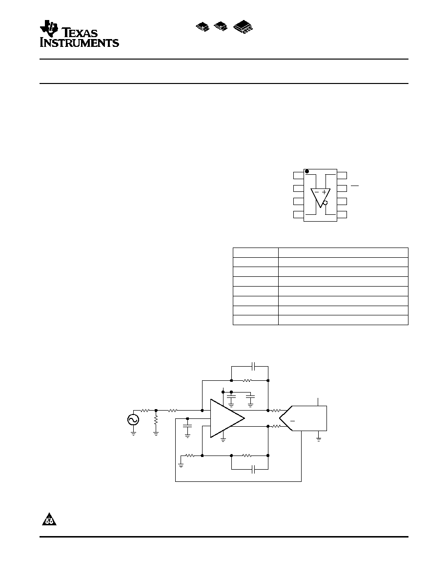
12 Bit/80 MSps
IN
IN
5 V
V
ref
5 V
V
S
0.1
µ
F
10
µ
F
499
8.2 pF
1
µ
F
53.6
ADC
487
50
523
499
8.2 pF
24.9
24.9
THS4504
THS4505
SLOS363C AUGUST 2002 REVISED MARCH 2004
WIDEBAND, LOW-DISTORTION, FULLY DIFFERENTIAL AMPLIFIERS
·
High Linearity Analog-to-Digital Converter
·
Fully Differential Architecture
Preamplifier
·
Bandwidth: 260 MHz
·
Wireless Communication Receiver Chains
·
Slew Rate: 1800 V/µs
·
Single-Ended to Differential Conversion
·
IMD
3
: -73 dBc at 30 MHz
·
Differential Line Driver
·
OIP
3
: 29 dBm at 30 MHz
·
Active Filtering of Differential Signals
·
Output Common-Mode Control
·
Wide Power Supply Voltage Range: 5 V,
±
5 V,
12 V, 15 V
·
Input Common-Mode Range Shifted to Include
the Negative Power Supply Rail
·
Power-Down Capability (THS4504)
·
Evaluation Module Available
DEVICE
(1)
DESCRIPTION
The THS4504 and THS4505 are high-performance
fully differential amplifiers from Texas Instruments.
THS4504/5
260 MHz, 1800 V/µs, V
ICR
Includes V
S-
The THS4504, featuring power-down capability, and
THS4500/1
370 MHz, 2800 V/µs, V
ICR
Includes V
S-
the THS4505, without power-down capability, set new
THS4502/3
370 MHz, 2800 V/µs, Centered V
ICR
performance standards for fully differential amplifiers
THS4120/1
3.3 V, 100 MHz, 43 V/µs, 3.7 nV
Hz
with
unsurpassed
linearity,
supporting
12-bit
THS4130/1
±
15 V, 150 MHz, 51 V/µs, 1.3 nV
Hz
operation through 40 MHz. Package options include
the
8-pin
SOIC
and
the
8-pin
MSOP
with
THS4140/1
±
15 V, 160 MHz, 450 V/µs, 6.5 nV
Hz
PowerPADTM for a smaller footprint, enhanced ac
THS4150/1
±
15 V, 150 MHz, 650 V/µs, 7.6 nV
Hz
performance,
and
improved
thermal
dissipation
capability.
(1)
Even numbered devices feature power-down capability
APPLICATION CIRCUIT DIAGRAM
Please be aware that an important notice concerning availability, standard warranty, and use in critical applications of Texas
Instruments semiconductor products and disclaimers thereto appears at the end of this data sheet.
PowerPAD is a trademark of Texas Instruments.
UNLESS OTHERWISE NOTED this document contains PRO-
Copyright © 20022004, Texas Instruments Incorporated
DUCTION DATA information current as of publication date. Prod-
ucts conform to specifications per the terms of Texas Instruments
standard warranty. Production processing does not necessarily
include testing of all parameters.
www.ti.com
ABSOLUTE MAXIMUM RATINGS
PACKAGE DISSIPATION RATINGS
RECOMMENDED OPERATING CONDITIONS
THS4504
THS4505
SLOS363C AUGUST 2002 REVISED MARCH 2004
These devices have limited built-in ESD protection. The leads should be shorted together or the device
placed in conductive foam during storage or handling to prevent electrostatic damage to the MOS gates.
over operating free-air temperature range unless otherwise noted
(1)
UNIT
Supply voltage, V
S
16.5 V
Input voltage, V
I
±
V
S
Output current, I
O
150 mA
Differential input voltage, V
ID
4 V
Continuous power dissipation
See Dissipation Rating Table
Maximum junction temperature, T
J
150
°
C
Maximum junction temperature, continuous operation, long-term reliability, T
J
(2)
125
°
C
Storage temperature range, T
stg
-65
°
C to 150
°
C
Lead temperature 1,6 mm (1/16 inch) from case for 10 seconds
300
°
C
(1)
The absolute maximum ratings under any condition is limited by the constraints of the silicon process. Stresses above these ratings may
cause permanent damage. Exposure to absolute maximum conditions for extended periods may degrade device reliability. These are
stress ratings only, and functional operation of the device at these or any other conditions beyond those specified is not implied.
(2)
The maximum junction temperature for continuous operation is limited by package constraints. Operation above this temperature may
result in reduced reliability and/or lifetime of the device.
POWER RATING
(2)
PACKAGE
JC
(
°
C/W)
JA
(
°
C/W)
(1)
T
A
25
°
C
T
A
= 85
°
C
D (8 pin)
38.3
97.5
1.02 W
410 mW
DGN (8 pin)
4.7
58.4
1.71 W
685 mW
DGK (8 pin)
54.2
260
385 mW
154 mW
(1)
This data was taken using the JEDEC standard High-K test PCB.
(2)
Power rating is determined with a junction temperature of 125
°
C. This is the point where distortion starts to substantially increase.
Thermal management of the final PCB should strive to keep the junction temperature at or below 125
°
C for best performance and long
term reliability.
MIN NOM
MAX
UNIT
Dual supply
±
5
±
7.5
Supply voltage
V
Single supply
4.5
5
15
Operating free-air temperature, T
A
-40
85
°
C
2

www.ti.com
PIN ASSIGNMENTS
THS4505
(TOP VIEW)
V
IN-
1
2
3
4
8
7
6
5
V
OCM
V
S+
V
OUT+
V
IN+
V
S-
V
OUT-
PD
D, DGK, AND DGN
THS4504
(TOP VIEW)
D DGK, AND DGN
V
IN-
1
2
3
4
8
7
6
5
V
OCM
V
S+
V
OUT+
V
IN+
V
S-
V
OUT-
NC
NC = No Internal Connection
See Note A.
THS4504
THS4505
SLOS363C AUGUST 2002 REVISED MARCH 2004
ORDERING INFORMATION
PACKAGED DEVICES
PACKAGE TYPE
PACKAGE MARKINGS
TRANSPORT MEDIA, QUANTITY
Power-down
THS4504D
Rails, 75
SOIC-8
--
THS4504DR
Tape and Reel, 2500
THS4504DGK
Rails, 100
MSOP-8
ASZ
THS4504DGKR
Tape and Reel, 2500
THS4504DGN
Rails, 80
MSOP-8-PP
(1)
BDB
THS4504DGNR
Tape and Reel, 2500
Non-power-down
THS4505D
Rails, 75
SOIC-8
--
THS4505DR
Tape and Reel, 2500
THS4505DGK
Rails, 100
MSOP-8
ATA
THS4505DGKR
Tape and Reel, 2500
THS4505DGN
Rails, 80
MSOP-8-PP
(1)
BDC
THS4505DGNR
Tape and Reel, 2500
(1)
The PowerPAD is electrically isolated from all other pins.
Note A: The devices with the power down option defaults to the ON state if no signal is applied to the PD pin.
3

www.ti.com
ELECTRICAL CHARACTERISTICS
THS4504
THS4505
SLOS363C AUGUST 2002 REVISED MARCH 2004
V
S
=
±
5 V, R
f
= R
g
= 499
, R
L
= 800
, G = +1, Single-ended input unless otherwise noted.
THS4504 AND THS4505
TYP
OVER TEMPERATURE
PARAMETER
TEST CONDITIONS
MIN/TYP
0
°
C to
-40
°
C to
/MAX
25
°
C
25
°
C
UNITS
70
°
C
85
°
C
AC PERFORMANCE
G = 1, P
IN
= -20 dBm, R
f
= 499
260
MHz
Typ
G = 2, P
IN
= -20 dBm, R
f
= 499
110
MHz
Typ
Small-signal bandwidth
G = 5, P
IN
= -20 dBm, R
f
= 499
40
MHz
Typ
G = 10, P
IN
= -20 dBm,
20
MHz
Typ
R
f
= 499
Gain-bandwidth product
G > +10
210
MHz
Typ
Bandwidth for 0.1dB flatness
P
IN
= -20 dBm
65
MHz
Typ
Large-signal bandwidth
G = 1, V
P
= 2 V
250
MHz
Typ
Slew rate
4 V
PP
Step
1800
V/µs
Typ
Rise time
2 V
PP
Step
0.8
ns
Typ
Fall time
2 V
PP
Step
1
ns
Typ
Settling time to 0.01%
V
O
= 4 V
PP
100
ns
Typ
0.1%
V
O
= 4 V
PP
20
ns
Typ
Harmonic distortion
G = 1, V
O
= 2 V
PP
Typ
f = 8 MHz
-79
dBc
Typ
2
nd
harmonic
f = 30 MHz
-66
dBc
Typ
f = 8 MHz
-93
dBc
Typ
3
rd
harmonic
f = 30 MHz
-65
dBc
Typ
V
O
= 2 V
PP
, f
c
= 30 MHz,
Third-order intermodulation
R
f
= 499
,
-73
dBc
Typ
distortion
200 kHz tone spacing
f
c
= 30 MHz, R
f
= 499
,
Third-order output intercept point
29
dBm
Typ
Referenced to 50
Input voltage noise
f > 1 MHz
8
nV/
Hz
Typ
Input current noise
f > 100 kHz
2
pA/
Hz
Typ
Overdrive recovery time
Overdrive = 5.5 V
60
ns
Typ
DC PERFORMANCE
Open-loop voltage gain
55
52
50
50
dB
Min
Input offset voltage
-4
-7 / -1
-8 / 0
-9 / +1
mV
Max
Average offset voltage drift
±
10
±
10
µV/
°
C
Typ
Input bias current
4
4.6
5
5.2
µA
Max
Average bias current drift
±
10
±
10
nA/
°
C
Typ
Input offset current
0.5
1
2
2
µA
Max
Average offset current drift
±
40
±
40
nA/
°
C
Typ
4
www.ti.com
THS4504
THS4505
SLOS363C AUGUST 2002 REVISED MARCH 2004
THS4504 AND THS4505
TYP
OVER TEMPERATURE
PARAMETER
TEST CONDITIONS
MIN/TYP
0
°
C to
-40
°
C to
/MAX
25
°
C
25
°
C
UNITS
70
°
C
85
°
C
INPUT
-5.7 /
Common-mode input range
-5.4 / 2.3
-5.1 / 2
-5.1 / 2
V
Min
2.6
Common-mode rejection ratio
80
74
70
70
dB
Min
Input impedance
10
7
|| 1
|| pF
Typ
OUTPUT
Differential output voltage swing
R
L
= 1 k
±
8
±
7.6
±
7.4
±
7.4
V
Min
Differential output current drive
R
L
= 20
130
110
100
100
mA
Min
Output balance error
P
IN
= -20 dBm, f = 100 kHz
-65
dB
Typ
Closed-loop output impedance
f = 1 MHz
0.1
Typ
(single-ended)
OUTPUT COMMON-MODE VOLTAGE CONTROL
Small-signal bandwidth
R
L
= 400
200
MHz
Typ
Slew rate
2 V
PP
step
92
V/µs
Typ
Minimum gain
1
0.98
0.98
0.98
V/V
Min
Maximum gain
1
1.02
1.02
1.02
V/V
Max
Common-mode offset voltage
-0.4
-4.6/+3.8
-6.6/+5.8
-7.6/+6.8
mV
Max
Input bias current
V
OCM
= 2.5 V
100
150
170
170
µA
Max
Input voltage range
±
4
±
3.7
±
3.4
±
3.4
V
Min
Input impedance
25 || 1
k
|| pF
Typ
Maximum default voltage
V
OCM
left floating
0
0.05
0.10
0.10
V
Max
Minimum default voltage
V
OCM
left floating
0
-0.05
-0.10
-0.10
V
Min
POWER SUPPLY
Specified operating voltage
±
5
±
7.5
±
7.5
±
7.5
V
Max
Maximum quiescent current
16
20
23
25
mA
Max
Minimum quiescent current
16
13
11
9
mA
Min
Power supply rejection (
±
PSRR)
80
76
73
70
dB
Min
POWER-DOWN (THS4504 ONLY)
Enable voltage threshold
Device enabled ON above -2.9 V
-2.9
V
Min
Device disabled OFF below
Disable voltage threshold
-4.3
V
Max
-4.3 V
Power-down quiescent current
800
1000
1200
1200
µA
Max
Input bias current
200
240
260
260
µA
Max
Input impedance
50 || 1
k
|| pF
Typ
Turnon time delay
1000
ns
Typ
Turnoff time delay
800
ns
Typ
5