www.ti.com
FEATURES
APPLICATIONS
DESCRIPTION
_
+
THS4302
R
f
100
49.9
V
I
+
22
µ
F
47 pF
0.1
µ
F
V
S+
50
Source
R
g
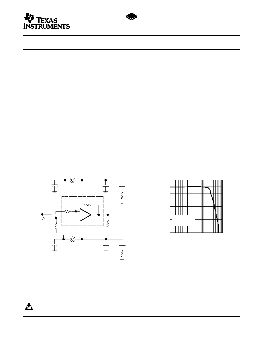
APPLICATION CIRCUIT
V
O
+
22
µ
F
47 pF
0.1
µ
F
V
S-
0
2
4
6
8
10
12
14
16
10 M
100 M
1 G
10 G
f - Frequency - Hz
Small Signal Gain - dB
SMALL SIGNAL FREQUENCY RESPONSE
V
O
= 200 mV
R
L
= 100
V
S
= 5 V
30.1
30.1
FB
FB
FB = Ferrite Bead
THS4302
SLOS403G OCTOBER 2002 REVISED JANUARY 2005
WIDEBAND FIXED-GAIN AMPLIFIER
·
Wideband Signal Processing
·
Fixed-Gain Closed-Loop Amplifier
·
Wireless Transceivers
·
Multiple Gain Options
·
IF Amplifier
THS4302: 5 V/V (14 dB)
·
ADC Preamplifier
·
Wide Bandwidth: 2.4 GHz
·
DAC Output Buffers
·
High Slew Rate: 5500 V/µs
·
Test, Measurement, and Instrumentation
·
Low Total Input Referred Noise: 2.8 nV/
Hz
·
Medical and Industrial Imaging
·
Low Distortion
HD
3
: -86 dBc at 30 MHz
HD
3
: -81 dBc at 70 MHz
The THS4302 device is a wideband, fixed-gain ampli-
IMD
3
: -88 dBc at 100 MHz
fier that offers high bandwidth, high slew rate, low
noise, and low distortion. This combination of specifi-
OIP
3
: 39 dBm at 100 MHz
cations enables analog designers to transcend cur-
IMD
3
: -73 dBc at 300 MHz
rent performance limitations and process analog sig-
OIP
3
: 32 dBm at 300 MHz
nals at much higher speeds than previously possible
with closed-loop, complementary amplifier designs.
·
High Output Drive:
±
180 mA
This device is offered in a 16-pin leadless package
·
Power Supply Voltage: 3 V or 5 V
and incorporates a power-down mode for quiescent
power savings.
Please be aware that an important notice concerning availability, standard warranty, and use in critical applications of Texas
Instruments semiconductor products and disclaimers thereto appears at the end of this data sheet.
PowerPAD is a trademark of Texas Instruments.
PRODUCTION DATA information is current as of publication date.
Copyright © 20022005, Texas Instruments Incorporated
Products conform to specifications per the terms of the Texas
Instruments standard warranty. Production processing does not
necessarily include testing of all parameters.

www.ti.com
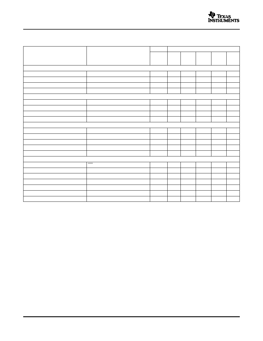
ABSOLUTE MAXIMUM RATING
RECOMMENDED OPERATING CONDITIONS
PACKAGE DISSIPATION RATINGS
THS4302
SLOS403G OCTOBER 2002 REVISED JANUARY 2005
These devices have limited built-in ESD protection. The leads should be shorted together or the device placed in conductive foam
during storage or handling to prevent electrostatic damage to the MOS gates.
over operating free-air temperature range unless otherwise noted
(1)
UNIT
Supply voltage, V
S
6 V
Input voltage, V
I
±
V
S
Output current, I
O
200 mA
Continuous power dissipation
See Dissipation Rating Table
Maximum junction temperature, T
J
150
°
C
Maximum junction temperature, continuous operation, long term reliability, T
J
(2)
125
°
C
Storage temperature range, T
stg
-65
°
C to 150
°
C
Lead temperature 1,6 mm (1/16 inch) from case for 10 seconds
300
°
C
(1)
The absolute maximum temperature under any condition is limited by the constraints of the silicon process. Stresses above these
ratings may cause permanent damage. Exposure to absolute maximum conditions for extended periods may degrade device reliability.
These are stress ratings only, and functional operation of the device at these or any other conditions beyond those specified is not
implied.
(2)
The maximum junction temperature for continuous operation is limited by package constraints. Operation above this temperature may
result in reduced reliability and/or lifetime of the device.
MIN
MAX
UNIT
Dual supply
±
1.5
±
2.5
Supply voltage, V
CC
(V
S+
and V
S-
)
V
Single supply
3
5
Common-mode input voltage range
V
S-
+1
V
S+
-1
V
POWER RATING
(2)
PACKAGE
JC
(
°
C/W)
JA
(
°
C/W)
(1)
T
A
25
°
C
T
A
= 25
°
C
RGT (16)
(3)
2.4
39.5
3.16
1.65 W
(1)
This data was taken using the JEDEC standard High-K test PCB.
(2)
Power rating is determined with a junction temperature of 125
°
C. This is the point where distortion starts to substantially increase.
Thermal management of the final PCB should strive to keep the junction temperature at or below 125
°
C for best performance and long
term reliability.
(3)
The THS4302 device may incorporate a PowerPADTM on the underside of the chip. This acts as a heatsink and must be connected to a
thermally dissipative plane for proper power dissipation. Failure to do so may result in exceeding the maximum junction temperature
which can permanently damage the device. See TI technical brief SLMA002 and SLMA004 for more information about utilizing the
PowerPAD thermally enhanced package.
AVAILABLE OPTIONS
INTERNAL FIXED GAIN
TRANSPORTATION MEDIA,
PACKAGED DEVICES
PACKAGE TYPE
(1)
RESISTOR VALUES (+5)
QUANTITY
R
G
R
F
THS4302RGTT
Tape and Reel, 250
Leadless (RGT-16)
50
200
THS4302RGTR
Tape and Reel, 3000
(1)
The PowerPAD is electrically isolated from all other pins.
2

www.ti.com
PIN ASSIGNMENTS
1
2
3
4
5
6
7
8
12
11
10
9
16 15 14 13
NC = No connect
V
S-
V
S
+
V
OUT
V
IN+
NC
PD
V
IN-
R
g
R
f
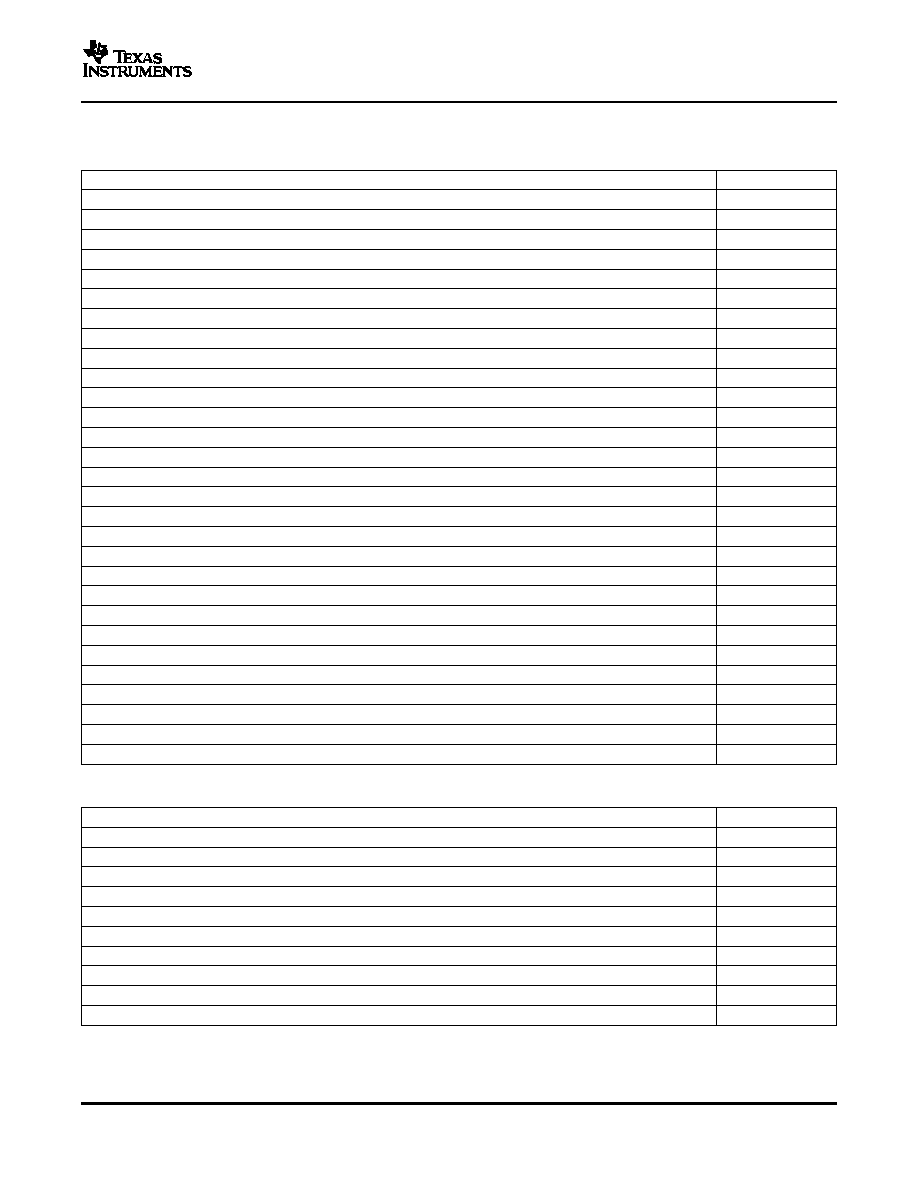
ELECTRICAL CHARACTERISTICS
THS4302
SLOS403G OCTOBER 2002 REVISED JANUARY 2005
RGT PACKAGE
TOP VIEW
THS4302 (Gain = +5 V/V) Specifications: V
S
= 5 V, R
L
= 100
, (unless otherwise noted)
TYP
OVERTEMPERATURE
MIN/
PARAMETER
TEST CONDITIONS
0
°
C to
-40
°
C
25
°
C
25
°
C
UNITS
TYP/
70
°
C
to 85
°
C
MAX
AC PERFORMANCE
Small signal bandwidth
G = +5, V
O
= 200 mV
RMS
2.4
GHz
Typ
Gain bandwidth product
12
GHz
Typ
Full-power bandwidth
G = +5, V
O
= 2 Vpp
875
MHz
Typ
Slew rate
G = +5, V
O
= 2 V Step
5500
V/µs
Min
Harmonic distortion
R
L
= 100
-66
dBc
Second harmonic distortion
Typ
G = +5, V
O
= 1 V
PP,
R
L
= 1 k
-75
dBc
f = 70 MHz
R
L
= 100
-81
dBc
Third harmonic distortion
Typ
R
L
= 1 k
-85
dBc
V
O
= 1 V
PP
envel-
f
c
= 100 MHz
-88
dBc
Third order intermoduation (IMD
3
)
ope, 200 kHz tone
Typ
f
c
= 300 MHz
-73
dBc
spacing
f
c
= 100 MHz
39
dBm
V
O
= 1 V
PP
, 200 kHz
Third order output intercept (OIP
3
)
Typ
tone spacing
f
c
= 300 MHz
32
dBm
Total input referred noise
f = 1 MHz
2.8
nV/
Hz
Typ
Noise figure
16
dB
Typ
DC PERFORMANCE
5
4.95
4.95
4.95
V/V
Min
Voltage gain
V
I
=
±
50 mV, V
CM
= 2.5 V
5
5.05
5.05
5.05
V/V
Max
Input offset voltage
V
CM
= 2.5 V
2
4.25
5.25
5.25
mV
Max
Average offset voltage drift
V
CM
= 2.5 V
±
20
±
20
µV/
°
C
Typ
Input bias current
V
CM
= 2.5 V
7
10
13
15
µA
Max
Average bias current drift
V
CM
= 2.5 V
±
55
±
55
nA/
°
C
Typ
3
www.ti.com
THS4302
SLOS403G OCTOBER 2002 REVISED JANUARY 2005
ELECTRICAL CHARACTERISTICS (continued)
THS4302 (Gain = +5 V/V) Specifications: V
S
= 5 V, R
L
= 100
, (unless otherwise noted)
TYP
OVERTEMPERATURE
MIN/
PARAMETER
TEST CONDITIONS
0
°
C to
-40
°
C
25
°
C
25
°
C
UNITS
TYP/
70
°
C
to 85
°
C
MAX
INPUT CHARACTERISTICS
Common-mode input range
0.5/4.5
1/4
1.1/3.9
1.2/3.8
V
Min
Common-mode rejection ratio
V
CM
= 2 V to 3 V
60
52
50
50
dB
Min
Input resistance
Noninverting input
1.6
M
Typ
Input capacitance
Noninverting input
1
pF
Max
OUTPUT CHARACTERISTICS
Output voltage swing
1/4
1.1/3.9
1.2/3.8
1.2/3.8
V
Min
Output current (sourcing)
R
L
= 5
180
170
165
160
mA
Min
Output current (sinking)
R
L
= 5
180
170
165
160
mA
Min
Output impedance
f = 10 MHz
0.2
Typ
POWER SUPPLY
Operating voltage
5
5.5
5.5
5.5
V
Max
Maximum quiescent current
37
42
46
48
mA
Max
Minimum quiescent current
37
32
29
26
mA
Min
Power supply rejection ratio (PSRR +)
V
S+
= 5 V to 4.5 V, V
S-
= 0 V
60
54
52
51
dB
Min
Power supply rejection ratio (PSRR -)
V
S+
= 5 V, V
S-
= 0 V to 0.5 V
75
65
64
62
dB
Min
POWER-DOWN CHARACTERISTICS
Maximum power-down current
PD = 0 V
0.8
1.0
1.1
1.2
mA
Max
Power-on voltage threshold
1.1
1.5
V
Min
Power-down voltage threshold
1.1
0.9
V
Max
Turnon time delay, t
d(on)
50% of final value
6
µs
Typ
Turnoff time delay, t
d(off)
50% of final value
5
µs
Typ
Input impedance
100
k
Typ
Output impedance
f = 100 kHz
250
Typ
4
www.ti.com
TYPICAL CHARACTERISTICS
Table of Graphs (5 V)
Table of Graphs (3 V)
THS4302
SLOS403G OCTOBER 2002 REVISED JANUARY 2005
FIGURE
S-Parameter vs Frequency
1
Small signal frequency response
2
Large signal frequency response
3
Slew rate vs Output voltage
4
Harmonic distortion vs Frequency
5, 6, 7, 8
Harmonic distortion vs Output voltage swing
9
Second-order intermodulation distortion vs Frequency
10
Second-order intercept point vs Frequency
11
Third order intermodulation distortion vs Frequency
12
Third-order intercept point vs Frequency
13
Voltage and current noise vs Frequency
14
Settling time
15, 16
Quiescent current vs Supply voltage
17
Output voltage vs Load resistance
18
Capacitive load frequency response
19
Gain vs Case temperature
20
Rejection ratios vs Frequency
21
Rejection ratios vs Case temperature
22
Common-mode rejection ratio vs Input common-mode range
23
Input offset voltage vs Case temperature
24
Positive input bias current vs Case temperature
25
Small signal transient response
26
Large signal transient response
27
Overdrive recovery
28
Closed-loop output impedance vs Frequency
29
Power-down quiescent current vs Supply voltage
30
Power-down output impedance vs Frequency
31
Turnon and turnoff delay times
32
Power-down S-Parameter vs Frequency
33
FIGURE
Small signal frequency response
34
Large signal frequency response
35
Slew rate vs Output voltage
36
Output voltage vs Load resistance
37
Capacitive load frequency response
38
Gain vs Case temperature
39
S - Parameter vs Frequency
40
Input offset voltage vs Case temperature
41
Positive input bias current vs Case temperature
42
Overdrive recovery
43
5