
DGK-8
DGN-8
D-8
DRB-8
www.ti.com
FEATURES
DESCRIPTION
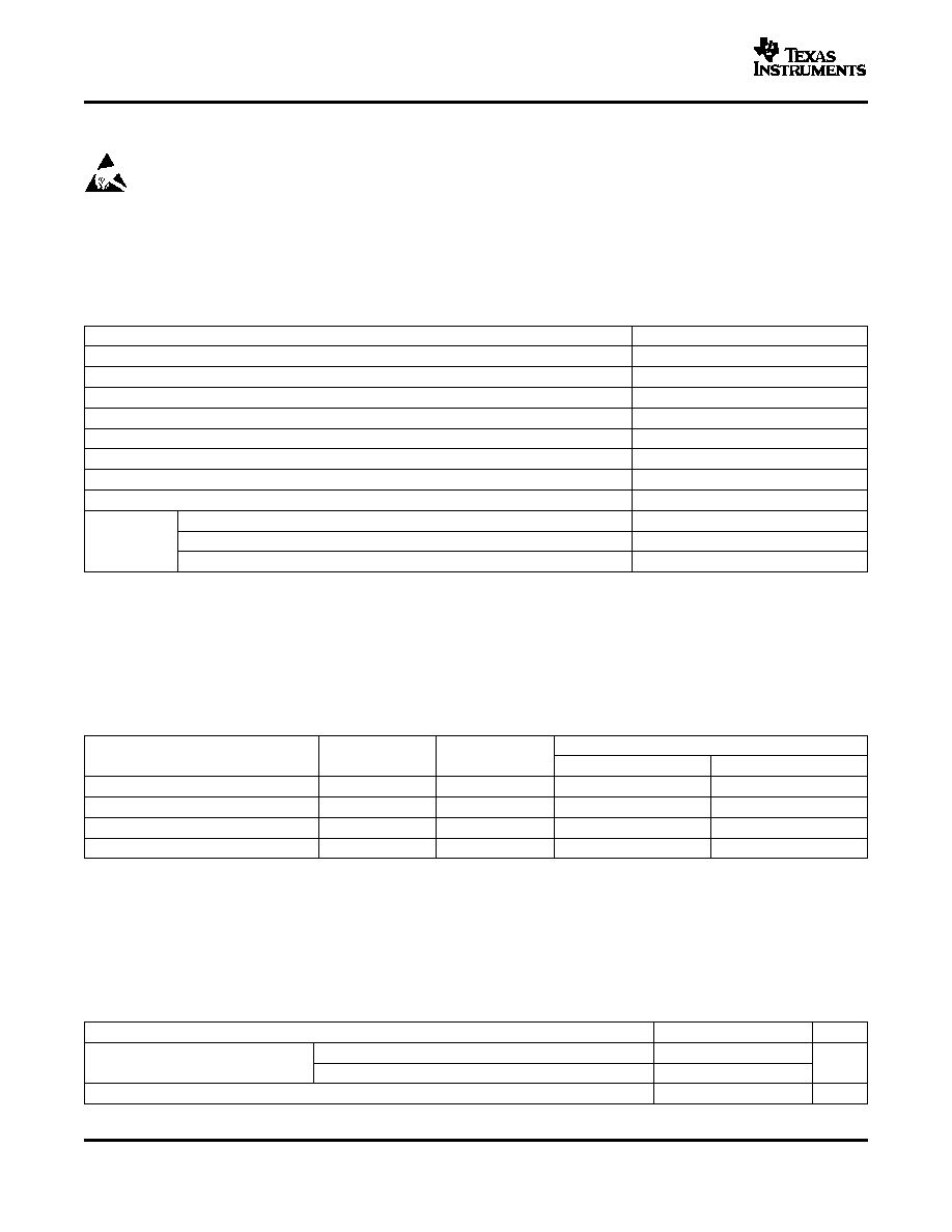
1
2
3
4
8
7
6
5
NC
IN-
IN+
V
S-
NC
V
S
+
V
OUT
NC
THS4211
APPLICATIONS
RELATED DEVICES
_
+
392
+5 V
49.9
V
I
-5 V
50
Source
Low-Distortion, Wideband Application Circuit
NOTE: Power supply decoupling capacitors not shown
V
O
392
50
THS4211
-100
-95
-90
-85
-80
-75
-70
-65
-60
-55
-50
1
10
100
Harmonic Distortion - dBc
HARMONIC DISTORTION
vs
FREQUENCY
f - Frequency - MHz
Gain = 2
R
f
= 392
R
L
= 150
V
O
= 2 V
PP
V
S
=
▒
5 V
HD2
HD3
THS4211
THS4215
SLOS400D ¡ SEPTEMBER 2002 ¡ REVISED NOVEMBER 2004
LOW-DISTORTION, HIGH-SPEED, VOLTAGE FEEDBACK AMPLIFIER
À
Unity Gain Stability
The THS4211 and THS4215 are high slew rate, unity
gain stable voltage feedback amplifiers designed to
À
Wide Bandwidth: 1 GHz
run from supply voltages as low as 5 V and as high
À
High Slew Rate: 970 V/Ás
as 15 V. The THS4215 offers the same performance
À
Low Distortion
as the THS4211 with the addition of power-down
¡ ¡90 dBc THD at 30 MHz
capability. The combination of high slew rate, wide
bandwidth, low distortion, and unity gain stability
¡ 130 MHz Bandwidth (0.1 dB, G = 2)
make the THS4211 and THS4215 high performance
¡ 0.007% Differential Gain
devices across multiple ac specifications.
¡ 0.003
░
Differential Phase
Designers using the THS4211 are rewarded with
À
High Output Drive, I
O
= 200 mA
higher dynamic range over a wider frequency band
À
Excellent Video Performance
without the stability concerns of decompensated
amplifiers. The devices are available in SOIC, MSOP
¡ 130 MHz Bandwidth (0.1 dB, G = 2)
with
PowerPADTM,
and
leadless
MSOP
with
¡ 0.007% Differential Gain
PowerPAD packages.
¡ 0.003
░
Differential Phase
À
Supply Voltages
¡ +5 V,
▒
5 V, +12 V, +15 V
À
Power Down Functionality (THS4215)
À
Evaluation Module Available
À
High Linearity ADC Preamplifier
À
Differential to Single-Ended Conversion
DEVICE
DESCRIPTION
À
DAC Output Buffer
THS4271
1.4 GHz voltage feedback amplifier
À
Active Filtering
THS4503
Wideband fully differential amplifier
À
Video Applications
THS3202
Dual, wideband current feedback amplifier
Please be aware that an important notice concerning availability, standard warranty, and use in critical applications of Texas
Instruments semiconductor products and disclaimers thereto appears at the end of this data sheet.
PowerPAD is a trademark of Texas Instruments.
PRODUCTION DATA information is current as of publication date.
Copyright ® 2002¡2004, Texas Instruments Incorporated
Products conform to specifications per the terms of the Texas
Instruments standard warranty. Production processing does not
necessarily include testing of all parameters.
www.ti.com
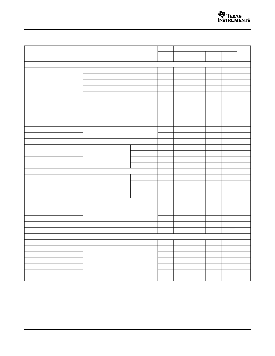
ABSOLUTE MAXIMUM RATINGS
PACKAGE DISSIPATION RATINGS
(1)
RECOMMENDED OPERATING CONDITIONS
THS4211
THS4215
SLOS400D ¡ SEPTEMBER 2002 ¡ REVISED NOVEMBER 2004
This integrated circuit can be damaged by ESD. Texas Instruments recommends that all integrated
circuits be handled with appropriate precautions. Failure to observe proper handling and installation
procedures can cause damage.
ESD damage can range from subtle performance degradation to complete device failure. Precision
integrated circuits may be more susceptible to damage because very small parametric changes could
cause the device not to meet its published specifications.
over operating free-air temperature range (unless otherwise noted)
(1)
UNIT
Supply voltage, V
S
16.5 V
Input voltage, V
I
▒
V
S
Output current, I
O
100 mA
Continuous power dissipation
See Dissipation Rating Table
Maximum junction temperature, T
J
(2)
150
░
C
Maximum junction temperature, continuous operation, long term reliability T
J
(3)
125
░
C
Storage temperature range, T
stg
¡65
░
C to 150
░
C
Lead temperature 1,6 mm (1/16 inch) from case for 10 seconds
300
░
C
HBM
4000 V
ESD ratings
CDM
1500 V
MM
200 V
(1)
Stresses above these ratings may cause permanent damage. Exposure to absolute maximum conditions for extended periods may
degrade device reliability. These are stress ratings only, and functional operation of the device at these or any other conditions beyond
those specified is not implied.
(2)
The absolute maximum ratings under any condition is limited by the constraints of the silicon process. Stresses above these ratings may
cause permanent damage. Exposure to absolute maximum conditions for extended periods may degrade device reliability. These are
stress ratings only, and functional operation of the device at these or any other conditions beyond those specified is not implied.
(3)
The maximum junction temperature for continuous operation is limited by package constraints. Operation above this temperature may
result in reduced reliability and/or lifetime of the device.
POWER RATING
(3)
JC
JA
(2)
PACKAGE
(
░
C/W)
(
░
C/W)
T
A
25
░
C
T
A
= 85
░
C
D (8 pin)
38.3
97.5
1.02 W
410 mW
DGN (8 pin)
(1)
4.7
58.4
1.71 W
685 mW
DGK (8 pin)
54.2
260
385 mW
154 mW
DRB (8 pin)
5
45.8
2.18 W
873 mW
(1)
The THS4211/5 may incorporate a PowerPADTM on the underside of the chip. This acts as a heat sink and must be connected to a
thermally dissipative plane for proper power dissipation. Failure to do so may result in exceeding the maximum junction temperature
which could permanently damage the device. See TI technical briefs SLMA002 and SLMA004 for more information about utilizing the
PowerPAD thermally enhanced package.
(2)
This data was taken using the JEDEC standard High-K test PCB.
(3)
Power rating is determined with a junction temperature of 125
░
C. This is the point where distortion starts to substantially increase.
Thermal management of the final PCB should strive to keep the junction temperature at or below 125
░
C for best performance and long
term reliability.
MIN
MAX
UNIT
Dual supply
▒
2.5
▒
7.5
Supply voltage, (V
S+
and V
S¡
)
V
Single supply
5
15
Input common-mode voltage range
V
S¡
+ 1.2
V
S+
¡ 1.2
V
2

www.ti.com
PIN ASSIGNMENTS
(TOP VIEW)
D, DRB, DGK, DGN
(TOP VIEW)
D, DRB, DGK, DGN
1
NC
NC
THS4211
2
3
4
8
7
6
5
IN -
IN +
V
S-
V
S
+
V
OUT
NC
1
REF
PD
THS4215
2
3
4
8
7
6
5
IN -
IN +
V
S-
V
S
+
V
OUT
NC
NC = No Connetion
NC = No Connection
See Note A.
THS4211
THS4215
SLOS400D ¡ SEPTEMBER 2002 ¡ REVISED NOVEMBER 2004
PACKAGING/ORDERING INFORMATION
PACKAGED DEVICES
PACKAGE TYPE
PACKAGE MARKING
TRANSPORT MEDIA, QUANTITY
Non-power-down
THS4211D
Rails, 75
SOIC-8
--
THS4211DR
Tape and Reel, 2500
THS4211DGK
Rails, 100
MSOP-8
BEJ
THS4211DGKR
Tape and Reel, 2500
THS4211DRBT
Tape and Reel, 250
QFN-8-PP
(1)
BET
THS4211DRBR
Tape and Reel, 3000
THS4211DGN
Rails, 80
MSOP-8-PP
(1)
BFN
THS4211DGNR
Tape and Reel, 2500
Power-down
THS4215D
Rails, 75
SOIC-8
--
THS4215DR
Tape and Reel, 2500
THS4215DGK
Rails, 100
MSOP-8
BEZ
THS4215DGKR
Tape and Reel, 2500
THS4215DRBT
Tape and Reel, 250
QFN-8-PP
(1)
BEU
THS4215DRBR
Tape and Reel, 3000
THS4215DGN
Rails, 80
MSOP-8-PP
(1)
BFQ
THS4215DGNR
Tape and Reel, 2500
(1)
The PowerPAD is electrically isolated from all other pins.
NOTE A: The devices with the power down option defaults to the ON state if no signal is applied to the PD pin.
3
www.ti.com
ELECTRICAL CHARACTERISTICS, V
S
=
▒
5 V
THS4211
THS4215
SLOS400D ¡ SEPTEMBER 2002 ¡ REVISED NOVEMBER 2004
R
F
= 392
, R
L
= 499
, G = +2, unless otherwise noted
TYP
OVER TEMPERATURE
MIN/
PARAMETER
TEST CONDITIONS
TYP/
0
░
C to
¡40
░
C
25
░
C
25
░
C
UNITS
MAX
70
░
C
to 85
░
C
AC PERFORMANCE
G = 1, P
OUT
= ¡7 dBm
1
GHz
Typ
G = ¡1, P
OUT
= ¡16 dBm
325
MHz
Typ
Small signal bandwidth
G = 2, P
OUT
= ¡16 dBm
325
MHz
Typ
G = 5, P
OUT
= ¡16 dBm
70
MHz
Typ
G = 10, P
OUT
= ¡16 dBm
35
MHz
Typ
0.1 dB flat bandwidth
G = 1, P
OUT
= ¡7 dBm
70
MHz
Typ
Gain bandwidth product
G > 10 , f = 1 MHz
350
MHz
Typ
Full-power bandwidth
G = ¡1, V
O
= 2 V
p
77
MHz
Typ
G = 1, V
O
= 2 V Step
970
V/Ás
Typ
Slew rate
G = ¡1, V
O
= 2 V Step
850
V/Ás
Typ
Settling time to 0.1%
22
ns
Typ
G = ¡1, V
O
= 4 V Step
Settling time to 0.01%
55
ns
Typ
Harmonic distortion
R
L
= 150
¡78
dBc
Typ
2
nd
-order harmonic distortion
R
L
= 499
¡90
dBc
Typ
G = 1, V
O
= 1 V
PP
,
f = 30 MHz
R
L
= 150
¡100
dBc
Typ
3
rd
-order harmonic distortion
R
L
= 499
¡100
dBc
Typ
Harmonic distortion
R
L
= 150
¡68
dBc
Typ
2
nd
-order harmonic distortion
R
L
= 499
¡70
dBc
Typ
G = 2, V
O
= 2 V
PP
,
f = 30 MHz
R
L
= 150
¡80
dBc
Typ
3
rd
-order harmonic distortion
R
L
= 499
¡82
dBc
Typ
3
rd
-order intermodulation (IMD
3
)
G = 2, V
O
= 2 V
PP
, R
L
= 150
, f = 70 MHz
¡53
dBc
Typ
3
rd
-order output intercept (OIP
3
)
G = 2, V
O
= 2 V
PP
, R
L
= 150
, f = 70 MHz
32
dBm
Typ
Differential gain (NTSC, PAL)
0.007
%
Typ
G = 2, R
L
= 150
Differential phase (NTSC, PAL)
0.003
░
Typ
Input voltage noise
f = 1 MHz
7
nV/
Hz
Typ
Input current noise
f = 10 MHz
4
pA
Hz
Typ
DC PERFORMANCE
Open-loop voltage gain (A
OL
)
V
O
=
▒
0.3 V, R
L
= 499
70
65
62
60
dB
Min
Input offset voltage
3
12
14
14
mV
Max
Average offset voltage drift
▒
40
▒
40
ÁV/
░
C
Typ
Input bias current
7
15
18
20
ÁA
Max
V
CM
= 0 V
Average bias current drift
▒
10
▒
10
nA/
░
C
Typ
Input offset current
0.3
6
7
8
ÁA
Max
Average offset current drift
▒
10
▒
10
nA/
░
C
Typ
4
www.ti.com
THS4211
THS4215
SLOS400D ¡ SEPTEMBER 2002 ¡ REVISED NOVEMBER 2004
TYP
OVER TEMPERATURE
MIN/
PARAMETER
TEST CONDITIONS
TYP/
0
░
C to
¡40
░
C
25
░
C
25
░
C
UNITS
MAX
70
░
C
to 85
░
C
INPUT CHARACTERISTICS
Common-mode input range
▒
4
▒
3.8
▒
3.7
▒
3.6
V
Min
Common-mode rejection ratio
V
CM
=
▒
1 V
56
52
50
48
dB
Min
Input resistance
Common-mode
4
M
Typ
Input capacitance
Common-mode/differential
0.3/0.2
pF
Typ
OUTPUT CHARACTERISTICS
Output voltage swing
▒
4.0
▒
3.8
▒
3.7
▒
3.6
V
Min
Output current (sourcing)
220
200
190
180
mA
Min
R
L
= 10
Output current (sinking)
170
140
130
120
mA
Min
Output impedance
f = 1 MHz
0.3
Typ
POWER SUPPLY
Specified operating voltage
▒
5
▒
7.5
▒
7.5
▒
7.5
V
Max
Maximum quiescent current
19
22
23
24
mA
Max
Minimum quiescent current
19
16
15
14
mA
Min
Power supply rejection (+PSRR)
V
S+
= 5.5 V to 4.5 V, V
S¡
= 5 V
64
58
54
54
dB
Min
Power supply rejection (¡PSRR)
V
S+
= 5 V, V
S¡
= ¡5.5 V to ¡4.5 V
65
60
56
56
dB
Min
POWER-DOWN CHARACTERISTICS (THS4215 ONLY)
Enable
REF+1.8
V
Min
REF = 0 V, or V
S¡
Power-down
REF+1
V
Max
Power-down voltage level
Enable
REF¡1
V
Min
REF = V
S+
or Floating
Power-down
REF¡1.5
V
Max
PD = Ref +1.0 V, Ref = 0 V
650
850
900
1000
ÁA
Max
Power-down quiescent current
PD = Ref ¡1.5 V, Ref = 5 V
450
650
800
900
ÁA
Max
Turnon time delay(t
(ON)
)
50% of final supply current value
4
Ás
Typ
Turnoff time delay (t
(Off)
)
50% of final supply current value
3
Ás
Typ
Input impedance
4
G
Typ
Output impedance
f = 1 MHz
250
k
Typ
5