SN75LVDS88
TFT LCD PANEL TIMING CONTROLLER
WITH LVDS INTERFACE
SLLS344 ¡ OCTOBER 1999
1
POST OFFICE BOX 655303
À
DALLAS, TEXAS 75265
D
Flatlink Interface Utilizes Low Power
Differential Signalling(LVDS)
D
Suitable for Notebook Application
D
XGA Resolution
D
Six Bit System Interface
D
Support Mainstream Data and Gate Drivers
D
Optional Configurable Pins
D
Low Voltage CMOS 3.3 V Technology
D
65 MHz Phase-Lock Input
D
100-pin TQFP Package for Compact LCD
Module
D
Tolerates 4 kV HBM ESD for LVDS Pins and
2 kV HBM for Others
D
Improved Jitter Tolerance
description
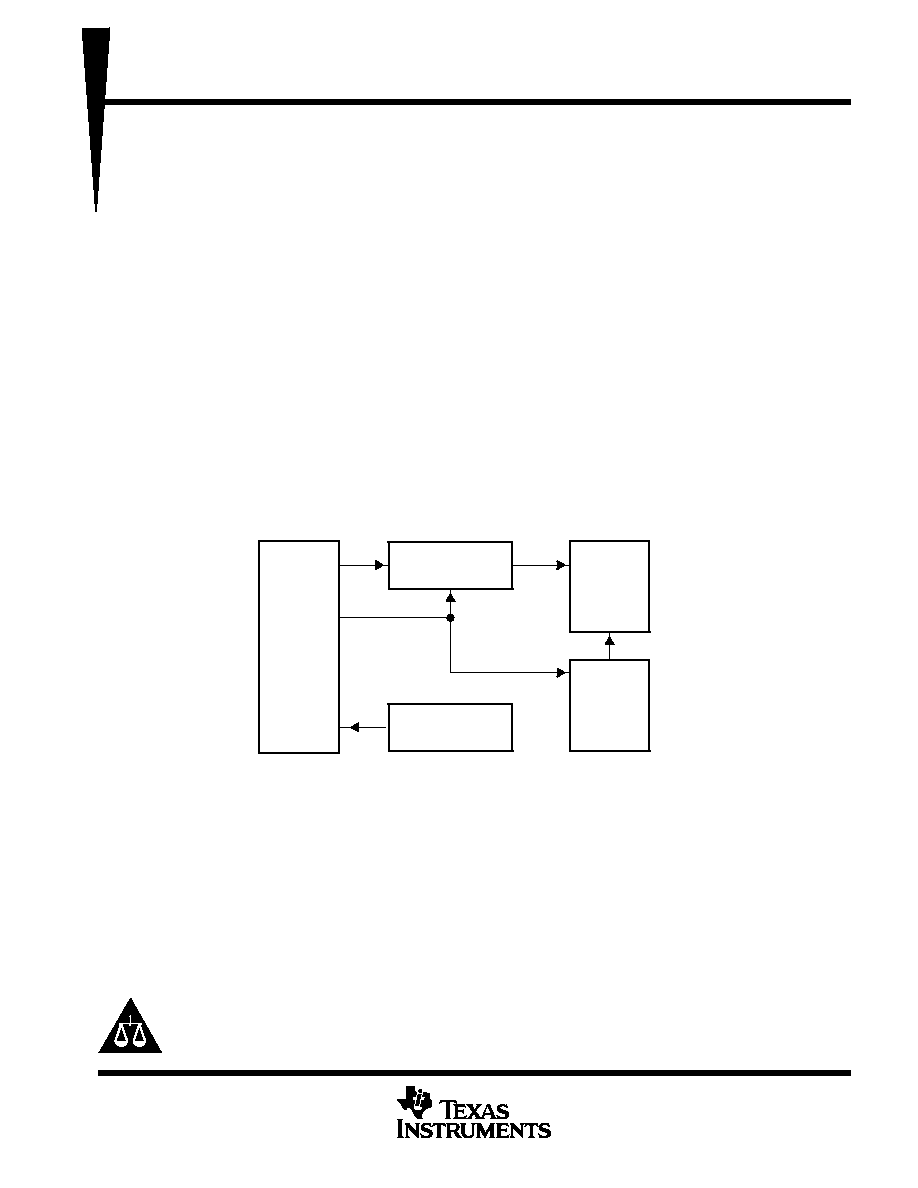
The SN75LVDS88 (LVDS panel timing controller) integrates a Flatlink signal interface with a TFT LCD timing
controller. It resides in the LCD panel and provides interface between the graphic controller and a TFT LCD
panel.
The SN75LVDS88 accepts host data through 3 pairs of inputs (18-bits) making up the LVDS bus, which is a
low-EMI high-throughput interface. SN75LVDS88 then reformats the received image data into a specific data
format and synchronous timing suitable for driving LCD panel column and row drivers. This device supports
XGA resolution.
The SN75LVDS88 is easily configured by several selection terminals and is equipped with default timing
specifications to support mainstream gate and source drivers on the market.
block diagram
Flat Link
(18-bit)
Timing
Signal
Generator
SYNC
Data Alignment
CTRL
Interface
Source
Data
Format
Copyright
®
1999, Texas Instruments Incorporated
PRODUCTION DATA information is current as of publication date.
Products conform to specifications per the terms of Texas Instruments
standard warranty. Production processing does not necessarily include
testing of all parameters.
Please be aware that an important notice concerning availability, standard warranty, and use in critical applications of
Texas Instruments semiconductor products and disclaimers thereto appears at the end of this data sheet.
SN75LVDS88
TFT LCD PANEL TIMING CONTROLLER
WITH LVDS INTERFACE
SLLS344 ¡ OCTOBER 1999
2
POST OFFICE BOX 655303
À
DALLAS, TEXAS 75265
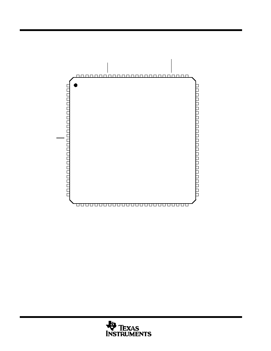
pin assignment
1
2
3
4
5
6
7
8
9
10
11
12
13
14
15
16
17
18
19
20
21
22
23
24
25
76
77
78
79
80
81
82
83
84
85
86
87
88
89
90
91
92
93
94
95
96
97
98
99
100
75
74
73
72
71
70
69
68
67
66
65
64
63
62
61
60
59
58
57
56
55
54
53
52
51
50
49
48
47
46
45
44
43
42
41
40
39
38
37
36
35
34
33
32
31
30
29
28
27
26
TEST1
MODE1
MODE0
VSS
POLEN
VDDA
RSTZ
GNDA
NC
CLKP
A2M
A1P
A1M
A0P
A0M
GNDD
SHTDN
VDDD
NC
NC
EG4
EG3
VDDIO
EG2
EG1
VSSIO
EG0
VDDIO
EB4(ER4)
VSSIO
EB2(ER2)
EB1(ER1)
VDDIO
EB0(ER0)
VSSIO
CLK
SP
VSSIO
OR4(OB4)
OR3(OB3)
EPOL
TQFP PACKAGE
(TOP VIEW)
CLKM
GND1
NC
EB5(ER5)
VDDIO
MODE2
TP1
CPV
VSS
STV
OE1
REV_E
VDD
REV_O
OE2
TP2
VSSIO
CLK
VDDIO
TEST2
ER5(EB5)
VSSIO
ER4(EB4)
ER3(EB3)
VDDIO
ER2(EB2)
ER1(EB1)
VSSIO
ER0(EB0)
EG5
VDD
OPOL
VSS
OB0(OR0)
VDD
OB1(OR1)
OB2(OR2)
VSSIO
OB3(OR3)
OB4(OR4)
VDDIO
OB5(OR5)
OG0
VSSIO
OG1
OG2
VDDIO
OG3
OG4
VSSIO
OG5
OR0(OB0)
VDDIO
OR1(OB1)
OR2(OB2)
EB3(ER3)
OR5(OB3)
DBS
A2P
SN75LVDS88

SN75LVDS88
TFT LCD PANEL TIMING CONTROLLER
WITH LVDS INTERFACE
SLLS344 ¡ OCTOBER 1999
3
POST OFFICE BOX 655303
À
DALLAS, TEXAS 75265
Terminal Functions
TERMINAL
I/O
DESCRIPTION
NAME
NO.
I/O
DESCRIPTION
A0M/A0P
81,82
I
Flatlink 1st data pair
A1M/A1P
83, 84
I
Flatlink 2nd data pair
A2M/A2P
85, 86
I
Flatlink 3rd data pair
CLK
44
O
CD bus clock
CLK
13
O
CD bus clock (180 degree out of phase)
CLKM/CLKP
87, 88
I
Flatlink clock pair
CPV
3
O
Gate driver clock
DBS
97
I
Data bus sequence
EPOL
42
O
Even RGB data stream polarity indicator
ER0..ER5
(EB0)..(EB5)
24,22,21
19,18,16
O
Even red (blue) data bus, controlled by DBS Pin, 0 = red, 1 = blue
(ER0)..(ER5)
EB0..EB5
41,39,38
36,35,33
O
Even blue (red) data bus, controlled by DBS Pin, 0 = blue, 1 = red
GND1
91
P
PLL ground for LVDS
MODE0
98
I
Default timing selection pin 0
MODE1
99
I
Default timing selection pin 1
MODE2
1
I
Default timing selection pin 2
NC
76, 77,
89, 90
NC
NC terminals
OE1, OE2
6, 10
O
Gate driver output enable
OG0..OG5
63,61,60
58,57,55
O
Odd green data bus
OPOL
74
O
Odd RGB data stream polarity indicator
OR0..OR5
(OB0)..(OB5)
54,52,51
50,49,47
O
Odd red (blue) data bus, controlled by DBS Pin, 0 = red, 1 = blue
(OR0)..(OR5)
OB0..OB5
72,70,69
67,66,64
O
Odd blue (red) data bus, controlled by DBS Pin, 0 = blue, 1 = red
POLEN
95
I
Output data polarity control enable /disable
REV_E
7
O
CD line/dot inversion control signal
REV_O
9
O
CD line/dot inversion control signal (180 degree of phase)
RSTZ
93
I
Reset, active low
SHTDN
79
I
System shutdown control, active low
SP
46
O
Data bus starting pulse
STV
5
O
Gate driver starting pulse
TEST1, TEST2
100, 15
I
Test points
TP1, TP2
2, 11
O
CD output control signal
VDDA
94
P
PLL power for LVDS
GNDA
92
P
Analog ground for LVDS
VDDD
78
P
Digital power supply for LVDS
GNDD
80
P
Digital power ground for LVDS
VDD
8,71,75
P
Digital power
VSS
4,73,96
P
Digital ground
VDDIO
P
I/O power
VSSIO
P
I/O ground
Terminals must be connected to ground.
SN75LVDS88
TFT LCD PANEL TIMING CONTROLLER
WITH LVDS INTERFACE
SLLS344 ¡ OCTOBER 1999
4
POST OFFICE BOX 655303
À
DALLAS, TEXAS 75265
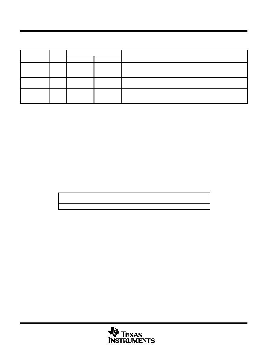
options
output control
PIN NAME
PIN NO
INTERNAL CONNECTION
DESCRIPTION
PIN NAME
PIN NO.
REQUIRED
SUGGESTED
DESCRIPTION
MODE0
MODE1
MODE2
98
99
1
Pull-up
Pull-up
Pull-down
Default timing selection pin 0
Default timing selection pin 1
Default timing selection pin 2
POLEN
Pull-down
0 = Output data reverse disable
1 = Output data reverse enable
DBS
97
Pull-down
Data bus sequence
0 = normal (RGB)
1 = reverse (BGR)
NOTE: DBS and POLEN functions must not be enabled together. The option pins must be connected to ground or VDD.
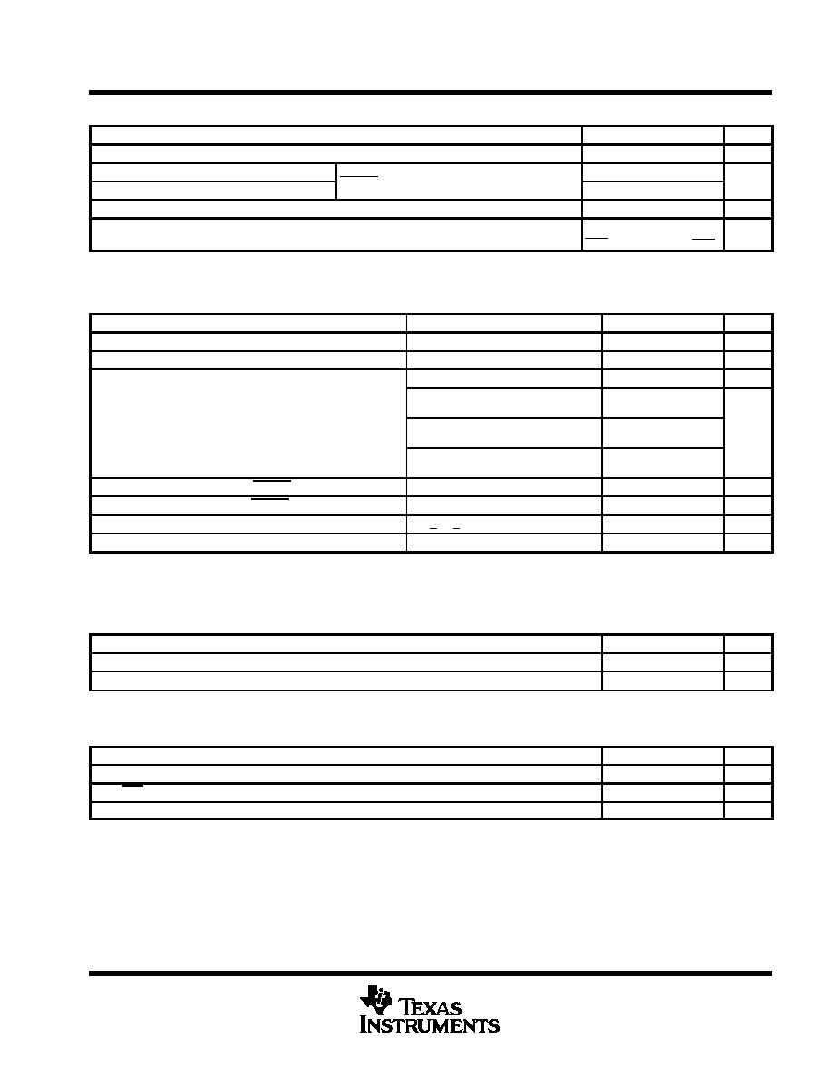
absolute maximum ratings over operating free-air temperature (unless otherwise noted)
Supply voltage range, V
CC
¡0.5 V to 4 V
. . . . . . . . . . . . . . . . . . . . . . . . . . . . . . . . . . . . . . . . . . . . . . . . . . . . . . . . .
Voltage range at any terminal
¡0.5 V to V
CC
+ 0.5 V
. . . . . . . . . . . . . . . . . . . . . . . . . . . . . . . . . . . . . . . . . . . . . . . . .
Continuous power dissipation
See Dissipation Rating Table
. . . . . . . . . . . . . . . . . . . . . . . . . . . . . . . . . . . . . . . . .
Storage temperature range, T
stg
¡65
░
C to 150
░
C
. . . . . . . . . . . . . . . . . . . . . . . . . . . . . . . . . . . . . . . . . . . . . . . . . . .
Electrostatic discharge:
Class 3 A
4 kV
. . . . . . . . . . . . . . . . . . . . . . . . . . . . . . . . . . . . . . . . . . . . . . . . . . . . . . . . . .
Class 2 B
200 V
. . . . . . . . . . . . . . . . . . . . . . . . . . . . . . . . . . . . . . . . . . . . . . . . . . . . . . . . .
Lead temperature 1,6 mm (1/16 inch) from case for 10 seconds
260
░
C
. . . . . . . . . . . . . . . . . . . . . . . . . . . . . . .
Stresses beyond those listed under "absolute maximum ratings" may cause permanent damage to the device. These are stress ratings only, and
functional operation of the device at these or any other conditions beyond those indicated under "recommended operating conditions" is not
implied. Exposure to absolute-maximum-rated conditions for extended periods may affect device reliability.
All voltage values are with respect to the GND terminals unless otherwise noted.
DISSIPATION RATING TABLE
PACKAGE
TA
25
░
C
POWER RATING
OPERATING FACTORº
ABOVE TA = 25
░
C
TA = 70
░
C
POWER RATING
PFD
1.548 W
12 mW
1.012 W
º This is the inverse of the junction-to-ambient thermal resistance when board-mounted and with
no air flow.
SN75LVDS88
TFT LCD PANEL TIMING CONTROLLER
WITH LVDS INTERFACE
SLLS344 ¡ OCTOBER 1999
5
POST OFFICE BOX 655303
À
DALLAS, TEXAS 75265
recommended operating conditions
MIN
NOM
MAX
UNIT
Supply voltage, VCC
3
3.3
3.6
V
High-level input voltage, VIH
SHTDN
2
V
Low-level input voltage, VIL
SHTDN
0.8
V
Magnitude of differential input voltage,
VID
0.1
0.6
V
Common¡mode input voltage, VIC
|V
ID
|
2
2.4 ¡
|V
ID
|
2
V
electrical characteristics over recommended operating free-air temperature range (unless
otherwise noted)
PARAMETER
TEST CONDITIONS
MIN
TYP
MAX
UNIT
VIT+
Positive-going differential input voltage threshold
100
mV
VIT¡
Negative-going differential input voltage threshold
¡100
mV
Disabled, all inputs to ground
360
Á
A
Enabled, AnP at 1 V and
AnM at 1.4 V, tC = 15.38 ns
80
ICC
Quiescent current (average)
Enabled, CL = 8 pF,
Grayscale pattern , tC = 15.38 ns
100
mA
Enabled, CL = 8 pF,
Worst-case pattern , tC = 15.38 ns
120
IIH
High-level input current (SHTDN)
VIH = VCC
▒
20
Á
A
IIL
Low-level input current (SHTDN)
VIL = 0 V
▒
20
Á
A
IIN
Input current (A inputs)
0 V < VI < 2.4 V
▒
20
Á
A
IOZ
High-impendance output current
VO = 0 V or VCC
▒
10
Á
A
All typical values are at VCC = 3.3 V, TA = 25
░
C.
The algebraic convention, in which the less-positive (more-negative) limit is designated minimum, is used in this data sheet for the negative-going
input voltage threshold only.
timing requirements
MIN
TYP
MAX
UNIT
tcº
Input clock period
14.7
31.25
ns
tsu/th
Input set up or hold time
550
ps
º tc is defined as the mean duration of a minimum of 32,000 clock periods.
output buffer rating
MIN
TYP
MAX
UNIT
STV, SP
4
mA
CLK, CLK
12
mA
Data bus and remaining outputs
8
mA