Document Outline
- FEATURES
- APPLICATIONS
- DESCRIPTION
- ORDERING INFORMATION
- PACKAGE DISSIPATION RATINGS (SEE FIGURE 12 AND FIGURE 13)
- ABSOLUTE MAXIMUM RATINGS
- RECOMMENDED OPERATING CONDITIONS
- DRIVER ELECTRICAL CHARACTERISTICS
- DRIVER SWITCHING CHARACTERISTICS NIL
- RECEIVER ELECTRICAL CHARACTERISTICS
- RECEIVER SWITCHING CHARACTERISTICS
- PARAMETER MEASUREMENT INFORMATION
- EQUIVALENT INPUT AND OUTPUT SCHEMATIC DIAGRAMS
- TYPICAL CHARACTERISTICS
- APPLICATION INFORMATION

SN65HVD05, SN65HVD06, SN65HVD07
SN75HVD05, SN75HVD06, SN75HVD07
SLLS533B MAY 2002 REVISED MAY 2003
HIGH OUTPUT RS-485 TRANSCEIVERS
FEATURES
D
Minimum Differential Output Voltage of 2.5 V
Into a 54-
Load
D
Open-Circuit, Short-Circuit, and Idle-Bus
Failsafe Receiver
D
1/8
th
Unit-Load Option Available (Up to 256
Nodes on the Bus)
D
Bus-Pin ESD Protection Exceeds 16 kV HBM
D
Driver Output Slew Rate Control Options
D
Electrically Compatible With ANSI
TIA/EIA-485-A Standard
D
Low-Current Standby Mode . . . 1
µ
A Typical
D
Glitch-Free Power-Up and Power-Down
Protection for Hot-Plugging Applications
D
Pin Compatible With Industry Standard
SN75176
APPLICATIONS
D
Data Transmission Over Long or Lossy Lines
or Electrically Noisy Environments
D
Profibus Line Interface
D
Industrial Process Control Networks
D
Point-of-Sale (POS) Networks
D
Electric Utility Metering
D
Building Automation
D
Digital Motor Control
DESCRIPTION
The SN65HVD05, SN75HVD05, SN65HVD06,
SN75HVD06, SN65HVD07, and SN75HVD07 combine
a 3-state differential line driver and differential line
receiver. They are designed for balanced data
transmission and interoperate with ANSI
TIA/EIA-485-A and ISO 8482E standard-compliant
devices. The driver is designed to provide a differential
output voltage greater than that required by these
standards for increased noise margin. The drivers and
receivers have active-high and active-low enables
respectively, which can be externally connected
together to function as direction control.
The driver differential outputs and receiver differential
inputs connect internally to form a differential input/
output (I/O) bus port that is designed to offer minimum
loading to the bus whenever the driver is disabled or not
powered. These devices feature wide positive and
negative common-mode voltage ranges, making them
suitable for party-line applications.
1
2
3
4
8
7
6
5
R
RE
DE
D
V
CC
B
A
GND
D OR P PACKAGE
(TOP VIEW)
0
0.5
1
1.5
2
2.5
3
3.5
4
4.5
5
0
20
40
60
80
100
120
Differential Output V
oltage
V
DIFFERENTIAL OUTPUT VOLTAGE
vs
DIFFERENTIAL OUTPUT CURRENT
V
O
IOD Differential Output Current mA
60
Load
Line
30
Load
Line
TA = 25
°
C
DE at VCC
D at VCC
VCC = 5 V
1
2
3
4
6
7
A
B
R
RE
DE
D
LOGIC DIAGRAM
(POSITIVE LOGIC)
PRODUCTION DATA information is current as of publication date. Products
conform to specifications per the terms of Texas Instruments standard warranty.
Production processing does not necessarily include testing of all parameters.
Please be aware that an important notice concerning availability, standard warranty, and use in critical applications of Texas Instruments
semiconductor products and disclaimers thereto appears at the end of this data sheet.
www.ti.com
Copyright
20022003, Texas Instruments Incorporated
SN65HVD05, SN65HVD06, SN65HVD07
SN75HVD05, SN75HVD06, SN75HVD07
SLLS533B MAY 2002 REVISED MAY 2003
www.ti.com
2
These devices have limited built-in ESD protection. The leads should be shorted together or the device placed in conductive foam during
storage or handling to prevent electrostatic damage to the MOS gates.
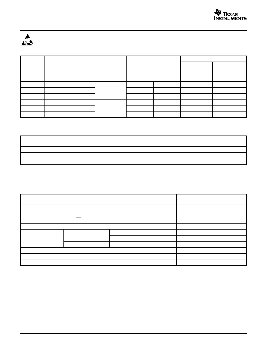
ORDERING INFORMATION
(1)
MARKED AS
SIGNALING
RATE
UNIT
LOAD
DRIVER
OUTPUT SLOPE
CONTROL
TA
PART NUMBER(2)
PLASTIC
DUAL-IN-LINE
PACKAGE
(PDIP)
SMALL OUTLINE
IC (SOIC)
PACKAGE
40 Mbps
1/2
No
SN65HVD05D
SN65HVD05P
65HVD05
VP05
10 Mbps
1/8
Yes
40
°
C to 85
°
C
SN65HVD06D
SN65HVD06P
65HVD06
VP06
1 Mbps
1/8
Yes
40 C to 85 C
SN65HVD07D
SN65HVD07P
65HVD07
VP07
40 Mbps
1/2
No
SN75HVD05D
SN75HVD05P
75HVD05
VN05
10 Mbps
1/8
Yes
0
°
C to 70
°
C
SN75HVD06D
SN75HVD06P
75HVD06
VN06
1 Mbps
1/8
Yes
0 C to 70 C
SN75HVD07D
SN75HVD07P
75HVD07
VN07
(1) For the most current specification and package information, refer to our web site at www.ti.com.
(2) The D package is available taped and reeled. Add an R suffix to the device type (i.e., SN65HVD05DR).
PACKAGE DISSIPATION RATINGS (SEE FIGURE 12 AND FIGURE 13)
PACKAGE
TA
25
°
C
POWER RATING
DERATING FACTOR(1)
ABOVE TA = 25
°
C
TA = 70
°
C
POWER RATING
TA = 85
°
C POWER
RATING
D(2)
710 mW
5.7 mW/
°
C
455 mW
369 mW
D(3)
1282 mW
10.3 mW/
°
C
821 mW
667 mW
P
1000 mW
8.0 mW/
°
C
640 mW
520 mW
(1) This is the inverse of the junction-to-ambient thermal resistance when board-mounted and with no air flow.
(2) Tested in accordance with the Low-K thermal metric definitions of EIA/JESD51-3
(3) Tested in accordance with the High-K thermal metric definitions of EIA/JESD51-7
ABSOLUTE MAXIMUM RATINGS
over operating free-air temperature range unless otherwise noted(1) (2)
SN65HVD05, SN65HVD06, SN65HVD07
SN75HVD05, SN75HVD06, SN75HVD07
Supply voltage range, VCC
0.3 V to 6 V
Voltage range at A or B
9 V to 14 V
Input voltage range at D, DE, R or RE
0.5 V to VCC + 0.5 V
Voltage input range, transient pulse, A and B, through 100
(see Figure 11)
50 V to 50 V
Human body model(3)
A, B, and GND
16 kV
Electrostatic discharge
Human body model(3)
All pins
4 kV
Electrostatic discharge
Charged-device model(4)
All pins
1 kV
Continuous total power dissipation
See Dissipation Rating Table
Storage temperature range, Tstg
65
°
C to 150
°
C
Lead temperature 1,6 mm (1/16 inch) from case for 10 seconds
260
°
C
(1) Stresses beyond those listed under "absolute maximum ratings" may cause permanent damage to the device. These are stress ratings only, and
functional operation of the device at these or any other conditions beyond those indicated under "recommended operating conditions" is not
implied. Exposure to absolute-maximum-rated conditions for extended periods may affect device reliability.
(2) All voltage values, except differential I/O bus voltages, are with respect to network ground terminal.
(3) Tested in accordance with JEDEC Standard 22, Test Method A114-A.
(4) Tested in accordance with JEDEC Standard 22, Test Method C101.
SN65HVD05, SN65HVD06, SN65HVD07
SN75HVD05, SN75HVD06, SN75HVD07
SLLS533B MAY 2002 REVISED MAY 2003
www.ti.com
3
RECOMMENDED OPERATING CONDITIONS
MIN
NOM
MAX
UNIT
Supply voltage, VCC
4.5
5.5
V
Voltage at any bus terminal (separately or common mode) VI or VIC
7(1)
12
V
High-level input voltage, VIH
D, DE, RE
2
V
Low-level input voltage, VIL
D, DE, RE
0.8
V
Differential input voltage, VID (see Figure 7)
12
12
V
High level output current I
Driver
100
mA
High-level output current, IOH
Receiver
8
mA
Low level output current I
Driver
100
mA
Low-level output current, IOL
Receiver
8
mA
SN65HVD05
SN65HVD06
40
85
°
C
Operating free air temperature T
SN65HVD07
40
85
C
Operating free-air temperature, TA
SN75HVD05
SN75HVD06
0
70
°
C
SN75HVD07
0
70
C
(1) The algebraic convention, in which the least positive (most negative) limit is designated as minimum is used in this data sheet.
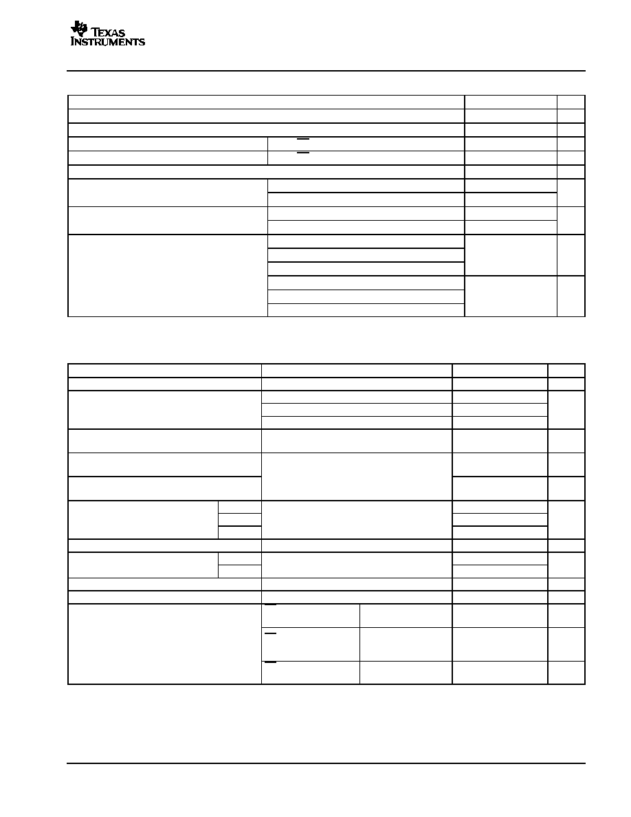
DRIVER ELECTRICAL CHARACTERISTICS
over operating free-air temperature range unless otherwise noted(1)
PARAMETER
TEST CONDITIONS
MIN
TYP(1)
MAX
UNIT
VIK
Input clamp voltage
II = 18 mA
1.5
V
No Load
VCC
|VOD|
Differential output voltage
RL = 54
, See Figure 1
2.5
V
|VOD|
Differential out ut voltage
Vtest = 7 V to 12 V, See Figure 2
2.2
V
|VOD|
Change in magnitude of differential
output voltage
See Figure 1 and Figure 2
0.2
0.2
V
VOC(SS)
Steady-state common-mode output
voltage
See Figure 3
2.2
3.3
V
VOC(SS)
Change in steady-state
common-mode output voltage
See Figure 3
0.1
0.1
V
Peak to peakcommon
HVD05
600
VOC(PP)
Peak-to-peak common-
mode output voltage
HVD06
See Figure 3
500
mV
VOC(PP)
mode output voltage
HVD07
See Figure 3
900
mV
IOZ
High-impedance output current
See receiver input currents
II
Input current
D
100
0
µ
A
II
Input current
DE
0
100
µ
A
IOS
Short-circuit output current
7 V
VO
12 V
250
250
mA
C(diff)
Differential output capacitance
VID = 0.4 sin (4E6
t) + 0.5 V, DE at 0 V
16
pF
RE at VCC,
D & DE at VCC, No load
Receiver disabled and
driver enabled
9
15
mA
ICC
Supply current
RE at VCC, D at VCC
DE at 0 V, No load
Receiver disabled and
driver disabled
(standby)
1
5
µ
A
RE at 0 V,
D & DE at VCC, No load
Receiver enabled and
driver enabled
9
15
mA
(1) All typical values are at 25
°
C and with a 5-V supply.
SN65HVD05, SN65HVD06, SN65HVD07
SN75HVD05, SN75HVD06, SN75HVD07
SLLS533B MAY 2002 REVISED MAY 2003
www.ti.com
4
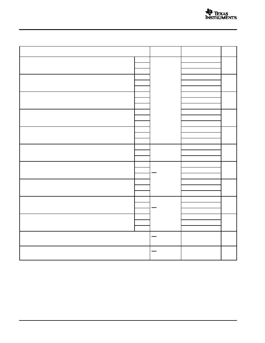
DRIVER SWITCHING CHARACTERISTICS NIL
over operating free-air temperature range unless otherwise noted
PARAMETER
TEST
CONDITIONS
MIN
TYP(1)
MAX
UNIT
HVD05
6.5
11
tPLH
Propagation delay time, low-to-high-level output
HVD06
27
40
ns
tPLH
Pro agation delay time, low to high level out ut
HVD07
250
400
ns
HVD05
6.5
11
tPHL
Propagation delay time, high-to-low-level output
HVD06
27
40
ns
tPHL
Pro agation delay time, high to low level out ut
HVD07
250
400
ns
HVD05
RL = 54
,
2.7
3.6
6
tr
Differential output signal rise time
HVD06
RL = 54
,
CL = 50 pF,
18
28
55
ns
tr
Differential out ut signal rise time
HVD07
CL 50 F,
See Figure 4
150
300
450
ns
HVD05
2.7
3.6
6
tf
Differential output signal fall time
HVD06
18
28
55
ns
tf
Differential out ut signal fall time
HVD07
150
300
450
ns
HVD05
2
tsk(p)
Pulse skew (|tPHL tPLH|)
HVD06
2.5
ns
tsk( )
Pulse skew (|tPHL tPLH|)
HVD07
10
ns
HVD05
3.5
tsk(pp)(2)
Part-to-part skew
HVD06
14
ns
tsk( )(2)
Part to art skew
HVD07
100
ns
HVD05
25
tPZH1
Propagation delay time, high-impedance-to-high-level output
HVD06
45
ns
tPZH1
Pro agation delay time, high im edance to high level out ut
HVD07
RE at 0 V,
RL 110
250
ns
HVD05
RL = 110
,
See Figure 5
25
tPHZ
Propagation delay time, high-level-to-high-impedance output
HVD06
See Figure 5
60
ns
tPHZ
Pro agation delay time, high level to high im edance out ut
HVD07
250
ns
HVD05
15
tPZL1
Propagation delay time, high-impedance-to-low-level output
HVD06
45
ns
tPZL1
Pro agation delay time, high im edance to low level out ut
HVD07
RE at 0 V,
RL 110
200
ns
HVD05
RL = 110
,
See Figure 6
14
tPLZ
Propagation delay time, low-level-to-high-impedance output
HVD06
See Figure 6
90
ns
tPLZ
Pro agation delay time, low level to high im edance out ut
HVD07
550
ns
tPZH2
Propagation delay time, standby-to-high-level output
RL = 110
,
RE at 3 V,
See Figure 5
6
µ
s
tPZL2
Propagation delay time, standby-to-low-level output
RL = 110
,
RE at 3 V,
See Figure 6
6
µ
s
(1) All typical values are at 25
°
C and with a 5-V supply.
(2) tsk(pp) is the magnitude of the difference in propagation delay times between any specified terminals of two devices when both devices operate
with the same supply voltages, at the same temperature, and have identical packages and test circuits.
SN65HVD05, SN65HVD06, SN65HVD07
SN75HVD05, SN75HVD06, SN75HVD07
SLLS533B MAY 2002 REVISED MAY 2003
www.ti.com
5
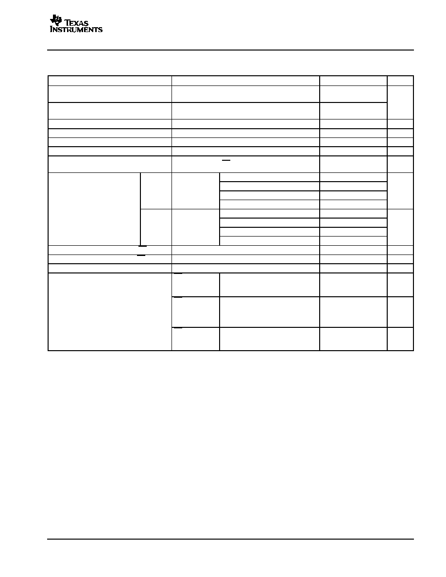
RECEIVER ELECTRICAL CHARACTERISTICS
over operating free-air temperature range unless otherwise noted
PARAMETER
TEST CONDITIONS
MIN
TYP(1)
MAX
UNIT
VIT+
Positive-going input threshold
voltage
IO = 8 mA
0.01
V
VIT
Negative-going input threshold
voltage
IO = 8 mA
0.2
V
Vhys
Hysteresis voltage (VIT+ VIT)
35
mV
VIK
Enable-input clamp voltage
II = 18 mA
1.5
V
VOH
High-level output voltage
VID = 200 mV,
IOH = 8 mA,
See Figure 7
4
V
VOL
Low-level output voltage
VID = 200 mV,
IOL = 8 mA,
See Figure 7
0.4
V
IOZ
High-impedance-state output
current
VO = 0 or VCC
RE at VCC
1
1
µ
A
VA or VB = 12 V
0.23
0.5
HVD05
Other input
VA or VB = 12 V,
VCC = 0 V
0.3
0.5
mA
HVD05
Other in ut
at 0 V
VA or VB = 7 V
0.4
0.13
mA
II
Bus input current
VA or VB = 7 V,
VCC = 0 V
0.4
0.15
II
Bus input current
VA or VB = 12 V
0.06
0.1
HVD06,
Other input
VA or VB = 12 V,
VCC = 0 V
0.08
0.13
mA
HVD06,
HVD07
Other in ut
at 0 V
VA or VB = 7 V
0.1
0.05
mA
VA or VB = 7 V,
VCC = 0 V
0.05
0.03
IIH
High-level input current, RE
VIH = 2 V
60
26.4
µ
A
IIL
Low-level input current, RE
VIL = 0.8 V
60
27.4
µ
A
C(diff)
Differential input capacitance
VI = 0.4 sin (4E6
t) + 0.5 V,
DE at 0 V
16
pF
RE at 0 V,
D & DE at 0 V,
No load
Receiver enabled and driver disabled
5
10
mA
ICC
Supply current
RE at VCC,
DE at 0 V,
D at VCC,
No load
Receiver disabled and driver disabled
(standby)
1
5
µ
A
RE at 0 V,
D & DE at VCC,
No load
Receiver enabled and driver enabled
9
15
mA
(1) All typical values are at 25
°
C and with a 5-V supply.