SN75468, SN75469
DARLINGTON TRANSISTOR ARRAYS
SLRS023B DECEMBER 1976 REVISED SEPTEMBER 1995
Copyright
©
1995, Texas Instruments Incorporated
31
POST OFFICE BOX 655303
·
DALLAS, TEXAS 75265
HIGH-VOLTAGE HIGH-CURRENT DARLINGTON TRANSISTOR ARRAYS
·
500-mA Rated Collector Current (Single
Output)
·
High-Voltage Outputs . . . 100 V
·
Output Clamp Diodes
·
Inputs Compatible With Various Types of
Logic
·
Relay Driver Applications
·
Higher-Voltage Versions of ULN2003A and
ULN2004A, for Commercial Temperature
Range
description
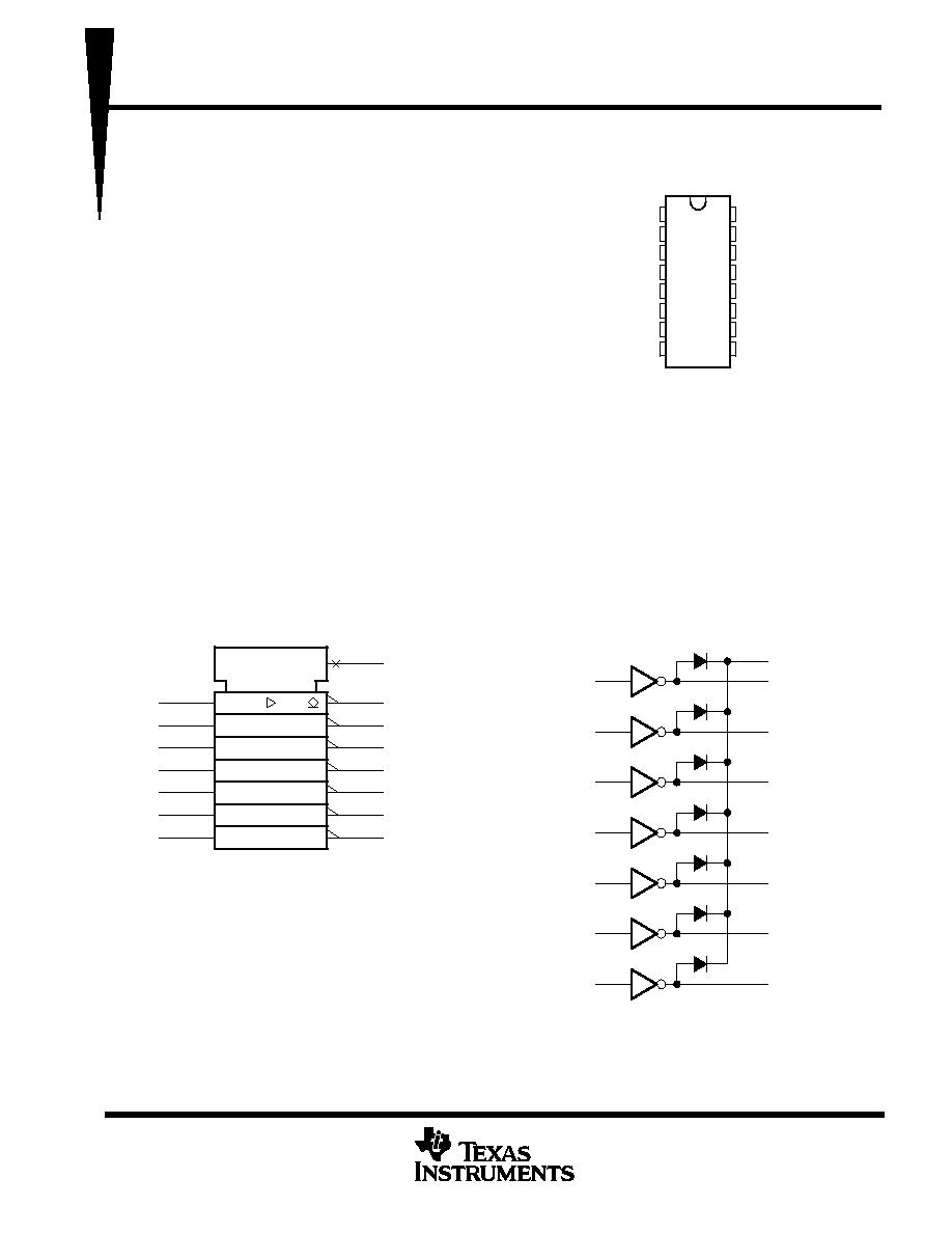
The SN75468 and SN75469 are monolithic high-voltage, high-current Darlington transistor arrays. Each
consists of seven npn Darlington pairs that feature high-voltage outputs with common-cathode clamp diodes
for switching inductive loads. The collector-current rating of each Darlington pair is 500 mA. The Darlington pairs
may be paralleled for higher current capability. Applications include relay drivers, hammer drivers, lamp drivers,
display drivers (LED and gas discharge), line drivers, and logic buffers.
The SN75468 has a 2700-
series base resistor for each Darlington pair for operation directly with TTL or 5-V
CMOS. The SN75469 has a 10.5-k
series base resistor to allow its operation directly with CMOS or PMOS
that use supply voltages of 6 to 15 V. The required input current is below that of the SN75468.
logic symbol
logic diagram
7B
6B
5B
4B
3B
2B
1B
7C
6C
5C
4C
3C
2C
1C
COM
7
6
5
4
3
2
1
10
11
12
13
14
15
16
9
7C
6C
5C
4C
3C
2C
1C
COM
7
6
5
4
3
2
1
7B
6B
5B
4B
3B
2B
1B
10
11
12
13
14
15
16
9
CLAMP
This symbol is in accordance with ANSI/IEEE
Std91-1984 and IEC publication 617-12.
1
2
3
4
5
6
7
8
16
15
14
13
12
11
10
9
1B
2B
3B
4B
5B
6B
7B
E
1C
2C
3C
4C
5C
6C
7C
COM
(TOP VIEW)
D OR N PACKAGE
PRODUCTION DATA information is current as of publication date.
Products conform to specifications per the terms of Texas Instruments
standard warranty. Production processing does not necessarily include
testing of all parameters.
SN75468, SN75469
DARLINGTON TRANSISTOR ARRAYS
SLRS023B DECEMBER 1976 REVISED SEPTEMBER 1995
32
POST OFFICE BOX 655303
·
DALLAS, TEXAS 75265
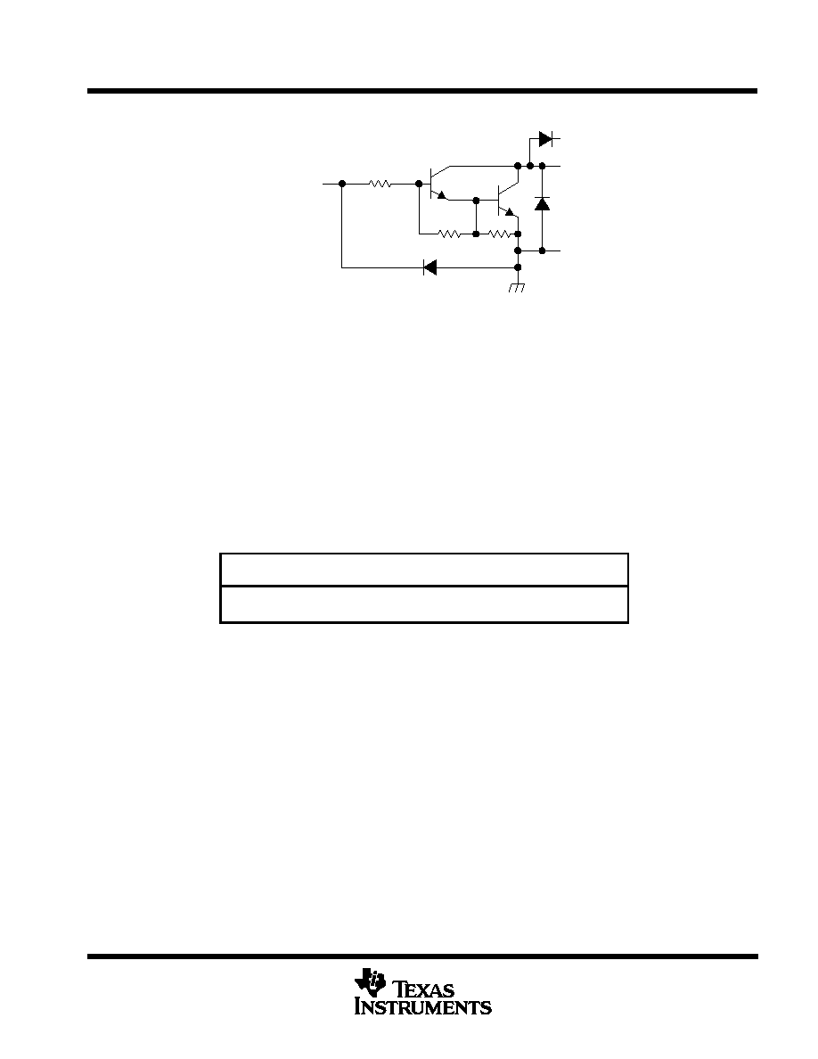
schematic (each Darlington pair)
COM
C
E
3 k
7.2 k
RB
B
SN75468: RB = 2.7 k
SN75469: RB = 10.5 k
All resistor values shown are nominal.
absolute maximum ratings at 25
°
C free-air temperature (unless otherwise noted)
Collector-emitter voltage, V
CE
100 V
. . . . . . . . . . . . . . . . . . . . . . . . . . . . . . . . . . . . . . . . . . . . . . . . . . . . . . . . . . . . .
Input voltage, V
I
(see Note 1)
30 V
. . . . . . . . . . . . . . . . . . . . . . . . . . . . . . . . . . . . . . . . . . . . . . . . . . . . . . . . . . . . . . .
Peak collector current (see Figures 14 and 15)
500 mA
. . . . . . . . . . . . . . . . . . . . . . . . . . . . . . . . . . . . . . . . . . . . .
Output clamp current, I
OK
500 mA
. . . . . . . . . . . . . . . . . . . . . . . . . . . . . . . . . . . . . . . . . . . . . . . . . . . . . . . . . . . . . . . .
Total emitter-terminal current
2.5 A
. . . . . . . . . . . . . . . . . . . . . . . . . . . . . . . . . . . . . . . . . . . . . . . . . . . . . . . . . . . . . .
Continuous total power dissipation
See Dissipation Rating Table
. . . . . . . . . . . . . . . . . . . . . . . . . . . . . . . . . . . . .
Operating free-air temperature range, T
A
0
°
C to 70
°
C
. . . . . . . . . . . . . . . . . . . . . . . . . . . . . . . . . . . . . . . . . . . . . .
Storage temperature range, T
stg
65
°
C to 150
°
C
. . . . . . . . . . . . . . . . . . . . . . . . . . . . . . . . . . . . . . . . . . . . . . . . . .
Lead temperature 1,6 mm (1/16 inch) from case for 10 seconds
260
°
C
. . . . . . . . . . . . . . . . . . . . . . . . . . . . . . .
NOTE 1: All voltage values are with respect to the emitter/substrate terminal E, unless otherwise noted.
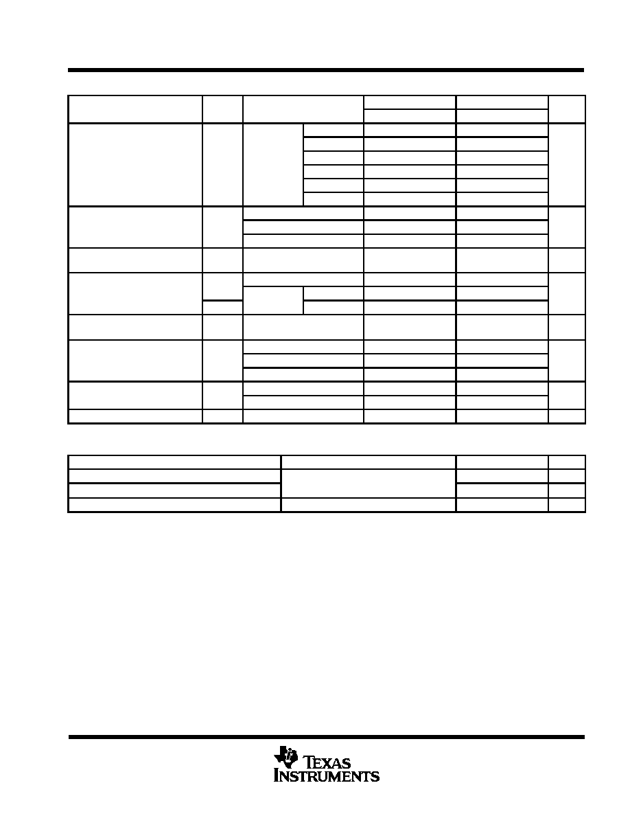
DISSIPATION RATING TABLE
PACKAGE
TA
25
°
C
POWER RATING
DERATING FACTOR
ABOVE TA = 25
°
C
TA = 70
°
C
POWER RATING
D
950 mW
7.6 mW/
°
C
608 mW
N
1150 mW
9.2 mW/
°
C
736 mW
SN75468, SN75469
DARLINGTON TRANSISTOR ARRAYS
SLRS023B DECEMBER 1976 REVISED SEPTEMBER 1995
33
POST OFFICE BOX 655303
·
DALLAS, TEXAS 75265
electrical characteristics, T
A
= 25
°
C (unless otherwise noted)
PARAMETER
TEST
TEST CONDITIONS
SN75468
SN75469
UNIT
PARAMETER
TEST
FIGURE
TEST CONDITIONS
MIN
TYP
MAX
MIN
TYP
MAX
UNIT
IC = 125 mA
5
IC = 200 mA
2.4
6
VI( )
On state input voltage
5
VCE = 2 V
IC = 250 mA
2.7
V
VI(on)
On-state input voltage
5
VCE = 2 V
IC = 275 mA
7
V
IC = 300 mA
3
IC = 350 mA
8
C ll
t
itt
II = 250
µ
A,
IC = 100 mA
0.9
1.1
0.9
1.1
VCE(sat)
Collector-emitter
saturation voltage
6
II = 350
µ
A,
IC = 200 mA
1
1.3
1
1.3
V
(
)
saturation voltage
II = 500
µ
A,
IC = 350 mA
1.2
1.6
1.2
1.6
VF
Clamp-diode forward
voltage
8
IF = 350 mA
1.7
2
1.7
2
V
1
VCE = 100 V,
II = 0
50
50
ICEX
Collector cutoff current
1
VCE = 100 V,
II = 0
100
100
µ
A
2
CE
,
TA = 70
°
C
VI = 1 V
500
II( ff)
Off state input current
3
VCE = 50 V,
IC = 500
µ
A,
50
65
50
65
µ
A
II(off)
Off-state input current
3
CE
,
TA = 70
°
C
C
µ
,
50
65
50
65
µ
A
VI = 3.85 V
0.93
1.35
II
Input current
4
VI = 5 V
0.35
0.5
mA
VI = 12 V
1
1.45
IR
Clamp-diode reverse
7
VR = 100 V
50
50
µ
A
IR
current
7
VR = 100 V,
TA = 70
°
C
100
100
µ
A
Ci
Input capacitance
VI = 0,
f = 1 MHz
15
25
15
25
pF
switching characteristics, T
A
= 25
°
C free-air temperature
PARAMETER
TEST CONDITIONS
MIN
TYP
MAX
UNIT
tPLH
Propagation delay time, low-to-high-level output
VS = 50 V,
RL = 163
,
CL = 15 pF,
0.25
1
µ
s
tPHL
Propagation delay time, high-to-low-level output
S
See Figure 9
L
L
0.25
1
µ
s
VOH
High-level output voltage after switching
VS = 50 V,
IO
300 mA,
See Figure 10
VS 20
mV
SN75468, SN75469
DARLINGTON TRANSISTOR ARRAYS
SLRS023B DECEMBER 1976 REVISED SEPTEMBER 1995
34
POST OFFICE BOX 655303
·
DALLAS, TEXAS 75265
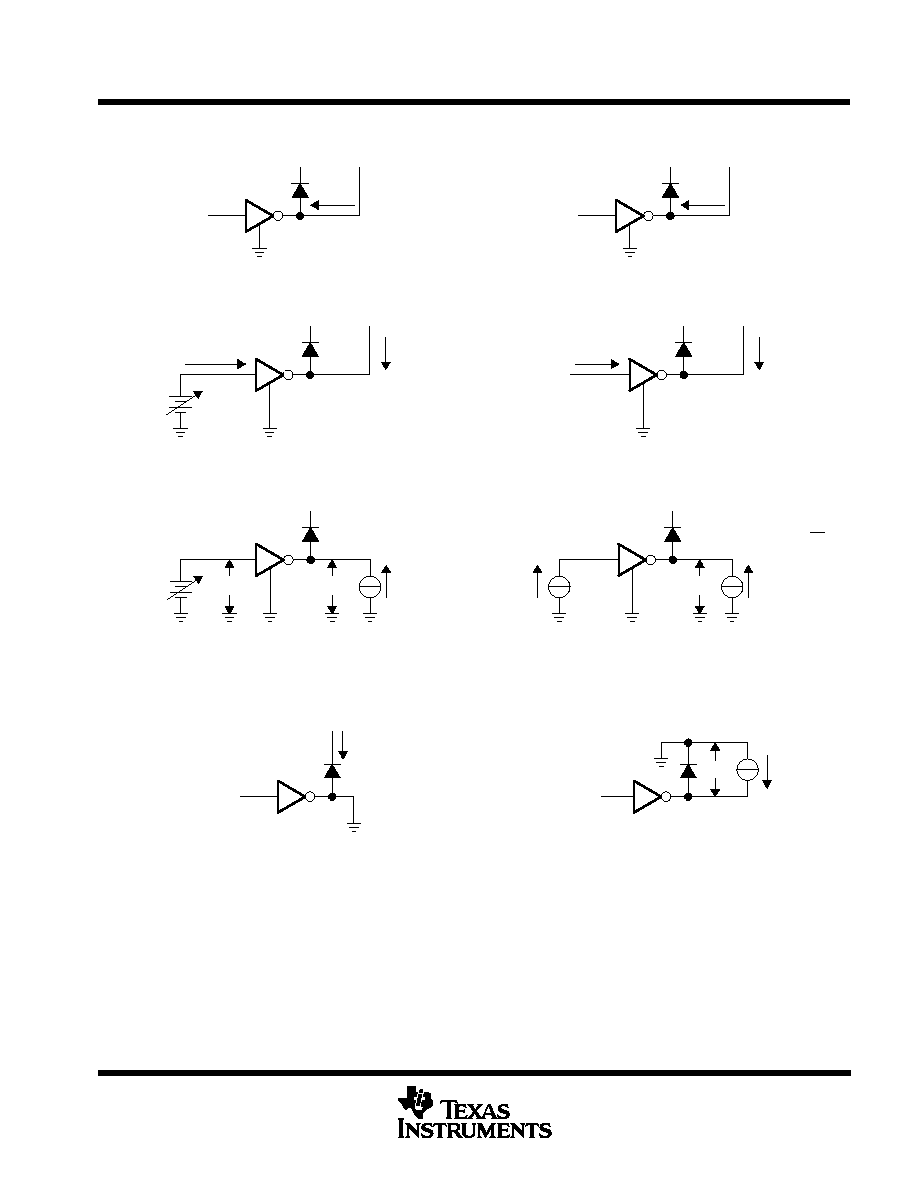
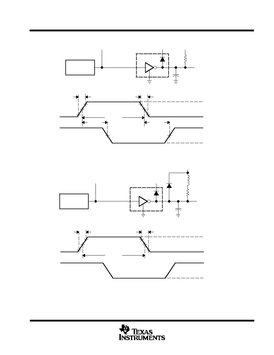
PARAMETER MEASUREMENT INFORMATION
Figure 1. I
CEX
Figure 2. I
CEX
VI
Open
Open
VCE
Open
ICEX
VCE
ICEX
Figure 3. I
I(off)
Figure 4. I
I
VI
II(on)
Open
IC
II(off)
Open
VCE
IC
VCE
NOTE: II is fixed for measuring VCE(sat),
variable for measuring hFE.
Figure 5. V
I(on)
Figure 6. h
FE
, V
CE(sat)
IC
II
VCE
VCE
VI(on)
Open
IC
Open
hFE =
IC
II
Figure 7. I
R
Figure 8. V
F
VF
IF
Open
IR
Open
VR
SN75468, SN75469
DARLINGTON TRANSISTOR ARRAYS
SLRS023B DECEMBER 1976 REVISED SEPTEMBER 1995
35
POST OFFICE BOX 655303
·
DALLAS, TEXAS 75265
PARAMETER MEASUREMENT INFORMATION
Input
Open
VS = 50 V
RL = 163
Output
CL = 15 pF
(see Note B)
90%
90%
50%
50%
10%
10%
50%
50%
tPHL
tPLH
0.5
µ
s
10 ns
5 ns
VIH
(see Note C)
0 V
VOH
VOL
Input
Output
TEST CIRCUIT
VOLTAGE WAVEFORMS
Pulse
Generator
(see Note A)
Figure 9. Test Circuit and Voltage Waveforms
Input
Open
VS
200
Output
CL = 15 pF
(see Note B)
90%
90%
1.5 V
1.5 V
10%
10%
40
µ
s
10 ns
5 ns
VIH
(see Note C)
0 V
VOH
VOL
Input
Output
TEST CIRCUIT
VOLTAGE WAVEFORMS
1N3064
2 mH
Pulse
Generator
(see Note A)
Figure 10. Latch-Up Test Circuit and Voltage Waveforms
NOTES: A. The pulse generator has the following characteristics: PRR = 12.5 kHz, ZO = 50
.
B. CL includes probe and jig capacitance.
C. For testing the '468, VIH = 3 V; for the '469, VIH = 8 V.