SN75179B
DIFFERENTIAL DRIVER AND RECEIVER PAIR
SLLS003E OCTOBER 1985 REVISED JUNE 1998
1
POST OFFICE BOX 655303
·
DALLAS, TEXAS 75265
D
Meets or Exceeds the Requirements of
TIA/EIA-422-B, TIA/EIA-485-A, and ITU
Recommendation V.11
D
Bus Voltage Range . . . 7 V to 12 V
D
Positive- and Negative-Current Limiting
D
Driver Output Capability . . . 60 mA Max
D
Driver Thermal-Shutdown Protection
D
Receiver Input Impedance . . . 12 k
Min
D
Receiver Input Sensitivity . . .
±
200 mV
D
Receiver Input Hysteresis . . . 50 mV Typ
D
Operates From Single 5-V Supply
D
Low Power Requirements
description
The SN75179B is a differential driver and receiver pair designed for balanced transmission-line applications
and meets TIA/EIA-422-B, TIA/EIA-485-A, and ITU Recommendation V.11. It is designed to improve the
performance of full-duplex data communications over long bus lines.
The SN75179B driver output provides limiting for both positive and negative currents. The receiver features high
input impedance, input hysteresis for increased noise immunity, and input sensitivity of
±
200 mV over a
common-mode input voltage range of 7 V to 12 V. The driver provides thermal shutdown for protection from
line fault conditions. Thermal shutdown is designed to occur at a junction temperature of approximately 150
°
C.
The SN75179B is designed to drive current loads of up to 60 mA maximum.
The SN75179B is characterized for operation from 0
°
C to 70
°
C.
Function Tables
DRIVER
INPUT
OUTPUTS
D
Y
Z
H
H
L
L
L
H
RECEIVER
DIFFERENTIAL INPUTS
OUTPUT
A B
R
VID
0.2 V
H
0.2 V < VID < 0.2 V
?
VID
0.2 V
L
Open
?
H = high level, L = low level, ? = indeterminate
Copyright
©
1998, Texas Instruments Incorporated
PRODUCTION DATA information is current as of publication date.
Products conform to specifications per the terms of Texas Instruments
standard warranty. Production processing does not necessarily include
testing of all parameters.
Please be aware that an important notice concerning availability, standard warranty, and use in critical applications of
Texas Instruments semiconductor products and disclaimers thereto appears at the end of this data sheet.
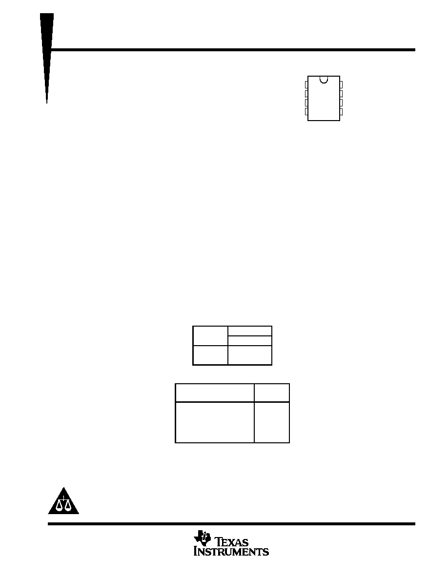
1
2
3
4
8
7
6
5
V
CC
R
D
GND
A
B
Z
Y
D OR P PACKAGE
(TOP VIEW)
SN75179B
DIFFERENTIAL DRIVER AND RECEIVER PAIR
SLLS003E OCTOBER 1985 REVISED JUNE 1998
2
POST OFFICE BOX 655303
·
DALLAS, TEXAS 75265
logic symbol
D
R
3
2
Y
Z
B
A
5
6
7
8
This symbol is in accordance with ANSI/IEEE Std 91-1984
and IEC Publication 617-12.
logic diagram (positive logic)
D
R
3
2
Y
Z
B
A
5
6
7
8
schematics of inputs and outputs
TYPICAL OF ALL RECEIVER OUTPUTS
TYPICAL OF ALL DRIVER OUTPUTS
EQUIVALENT OF EACH RECEIVER INPUT
EQUIVALENT OF DRIVER INPUT
Output
VCC
85
NOM
Input
VCC
16.8 k
NOM
960
NOM
GND
Output
VCC
Driver input: R(eq) = 3 k
NOM
R(eq) = equivalent resistor
Input
VCC
960
NOM
SN75179B
DIFFERENTIAL DRIVER AND RECEIVER PAIR
SLLS003E OCTOBER 1985 REVISED JUNE 1998
3
POST OFFICE BOX 655303
·
DALLAS, TEXAS 75265
absolute maximum ratings over operating free-air temperature range (unless otherwise noted)
Supply voltage, V
CC
(see Note 1)
7 V
. . . . . . . . . . . . . . . . . . . . . . . . . . . . . . . . . . . . . . . . . . . . . . . . . . . . . . . . . . . . .
Voltage range at any bus terminal
10 V to 15 V
. . . . . . . . . . . . . . . . . . . . . . . . . . . . . . . . . . . . . . . . . . . . . . . . . . . .
Differential input voltage, V
ID
(see Note 2)
±
25 V
. . . . . . . . . . . . . . . . . . . . . . . . . . . . . . . . . . . . . . . . . . . . . . . . . . .
Package thermal impedance,
JA
(see Note 3): D package
197
°
C/W
. . . . . . . . . . . . . . . . . . . . . . . . . . . . . . . . . .
P package
104
°
C/W
. . . . . . . . . . . . . . . . . . . . . . . . . . . . . . . . . .
Storage temperature range, T
stg
65
°
C to 150
°
C
. . . . . . . . . . . . . . . . . . . . . . . . . . . . . . . . . . . . . . . . . . . . . . . . . . .
Lead temperature 1,6 mm (1/16 inch) from case for 10 seconds
260
°
C
. . . . . . . . . . . . . . . . . . . . . . . . . . . . . . .
Stresses beyond those listed under "absolute maximum ratings" may cause permanent damage to the device. These are stress ratings only, and
functional operation of the device at these or any other conditions beyond those indicated under "recommended operating conditions" is not
implied. Exposure to absolute-maximum-rated conditions for extended periods may affect device reliability.
NOTES:
1. All voltage values, except differential input voltage, are with respect to network ground terminal.
2. Differential input voltage is measured at the noninverting input with respect to the corresponding inverting input.
3. The package thermal impedance is calculated in accordance with JESD 51, except for through-hole packages, which use a trace
length of zero.
recommended operating conditions
MIN
NOM
MAX
UNIT
Supply voltage, VCC
4.75
5
5.25
V
High-level input voltage, VIH
Driver
2
V
Low-level input voltage, VIL
Driver
0.8
V
Common-mode input voltage, VIC
7
12
V
Differential input voltage, VID
±
12
V
High level output current IOH
Driver
60
mA
High-level output current, IOH
Receiver
400
µ
A
Low level output current IOL
Driver
60
mA
Low-level output current, IOL
Receiver
8
mA
Operating free-air temperature, TA
0
70
°
C
The algebraic convention, where the less positive (more negative) limit is designated minimum, is used in this data sheet for common-mode input
voltage and threshold voltage.

SN75179B
DIFFERENTIAL DRIVER AND RECEIVER PAIR
SLLS003E OCTOBER 1985 REVISED JUNE 1998
4
POST OFFICE BOX 655303
·
DALLAS, TEXAS 75265
DRIVER SECTION
electrical characteristics over recommended ranges of supply voltage and operating free-air
temperature (unless otherwise noted)
PARAMETER
TEST CONDITIONS
MIN
TYP
MAX
UNIT
VIK
Input clamp voltage
II = - 18 mA
1.5
V
VO
Output voltage
IO = 0
0
6
V
VOD1
Differential output voltage
IO = 0
1.5
6
V
VOD2
Differential output voltage
RL = 100
,
See Figure 1
1/2VOD1
or 2
V
OD2
g
RL = 54
,
See Figure 1
1.5
2.5
5
V
VOD3
Differential output voltage
See Note 4
1.5
5
V
VOD
Change in magnitude of common-mode
output voltage§
±
0.2
V
VOC
Common-mode output voltage
RL = 54
or 100
,
See Figure 1
3
1
V
VOC
Change in magnitude of common-mode
output voltage§
±
0.2
V
IO
Output current
VCC = 0,
VO = 7 V to 12 V
±
100
µ
A
IIH
High-level input current
VI = 2.4 V
20
µ
A
IIL
Low-level input current
VI = 0.4 V
200
µ
A
IOS
Short circuit output current
VO = 7 V
250
mA
IOS
Short-circuit output current
VO = VCC or 12 V
250
mA
ICC
Supply current (total package)
No load
57
70
mA
All typical values are at VCC = 5 V and TA = 25
°
C.
The minimum VOD2 with 100-
load is either 1/2 VOD2 or 2 V, whichever is greater.
§
|VOD| and
|VOC| are the changes in magnitude of VOD and VOC, respectively, that occur when the input changes from a high level to a low
level.
NOTE 4: See TIA/EIA-485-A, Figure 3.5, Test Termination Measurement 2.
switching characteristics, V
CC
= 5 V, T
A
= 25
°
C
PARAMETER
TEST CONDITIONS
MIN
TYP
MAX
UNIT
td(OD)
Differential output delay time
RL = 54
See Figure 3
15
22
ns
tt(OD)
Differential output transition time
RL = 54
,
See Figure 3
20
30
ns
Symbol Equivalents
DATA-SHEET PARAMETER
TIA/EIA-422-B
TIA/EIA-485-A
VO
Voa, Vob
Voa, Vob
| VOD1 |
Vo
Vo
| VOD2 |
Vt (RL = 100
)
Vt (RL = 54
)
| VOD3 |
Vt (Test Termination Measurement 2)
| VOD |
| | Vt | |Vt | |
| | Vt | |Vt | |
VOC
| Vos |
| Vos |
| VOC |
| Vos Vos |
| Vos Vos |
IOS
| Isa |, | Isb |
IO
| Ixa |, | Ixb |
Iia , Iib
SN75179B
DIFFERENTIAL DRIVER AND RECEIVER PAIR
SLLS003E OCTOBER 1985 REVISED JUNE 1998
5
POST OFFICE BOX 655303
·
DALLAS, TEXAS 75265
RECEIVER SECTION
electrical characteristics over recommended ranges of common-mode input voltage, supply
voltage, and operating free-air temperature (unless otherwise noted)
PARAMETER
TEST CONDITIONS
MIN
TYP
MAX
UNIT
VIT +
Positive-going input threshold voltage
VO = 2.7 V,
IO = 0.4 mA
0.2
V
VIT
Negative-going input threshold voltage
VO = 0.5 V,
IO = 8 mA
0.2
V
Vhys
Hysteresis voltage (VIT + VIT )
50
mV
VOH
High-level output voltage
VID = 200 mV,
IOH = 400
µ
A,
See Figure 2
2.7
V
VOL
Low-level output voltage
VID = 200 mV,
IOL = 8 mA,
See Figure 2
0.45
V
II
Line input current
Other input at 0 V
See Note 5
VI = 12 V
1
mA
II
Line input current
Other input at 0 V,
See Note 5
VI = 7 V
0.8
mA
ri
Input resistance
12
k
IOS
Short-circuit output current
15
85
mA
ICC
Supply current (total package)
No load
57
70
mA
All typical values are at VCC = 5 V, TA = 25
°
C.
The algebraic convention, where the less positive (more negative) limit is designated minimum, is used in this data sheet for common-mode input
voltage and threshold voltage levels only.
NOTE 5: Refer to TIA/EIA-422-B for exact conditions.
switching characteristics, V
CC
= 5 V, T
A
= 25
°
C
PARAMETER
TEST CONDITIONS
MIN
TYP
MAX
UNIT
tPLH
Propagation delay time, low- to high-level output
VID = 1.5 V to 1.5 V,
19
35
ns
tPHL
Propagation delay time, high- to low-level output
ID
CL = 15 pF, See Figure 4
30
40
ns
PARAMETER MEASUREMENT INFORMATION
VOD2
RL
2
VOC
RL
2
Figure 1. Driver V
DD
and V
OC
VID
IOH
VOH
+ IOL
VOL
Figure 2. Receiver V
OH
and V
OL