SN74LVCZ32245A
32 BIT BUS TRANSCEIVER
WITH 3 STATE OUTPUTS
SCES423 JANUARY 2003
1
POST OFFICE BOX 655303
·
DALLAS, TEXAS 75265
D
Member of the Texas Instruments
Widebus+
Family
D
Operates From 2.7 V to 3.6 V
D
Inputs Accept Voltages to 5.5 V
D
Max t
pd
of 3.7 ns at 3.3 V
D
I
off
and Power-Up 3-State Support Hot
Insertion
D
Supports Mixed-Mode Signal Operation on
All Ports (5-V Input/Output Voltage With
3.3-V V
CC
)
D
Latch-Up Performance Exceeds 100 mA Per
JESD 78, Class II
D
ESD Protection Exceeds JESD 22
2000-V Human-Body Model (A114-A)
1000-V Charged-Device Model (C101)
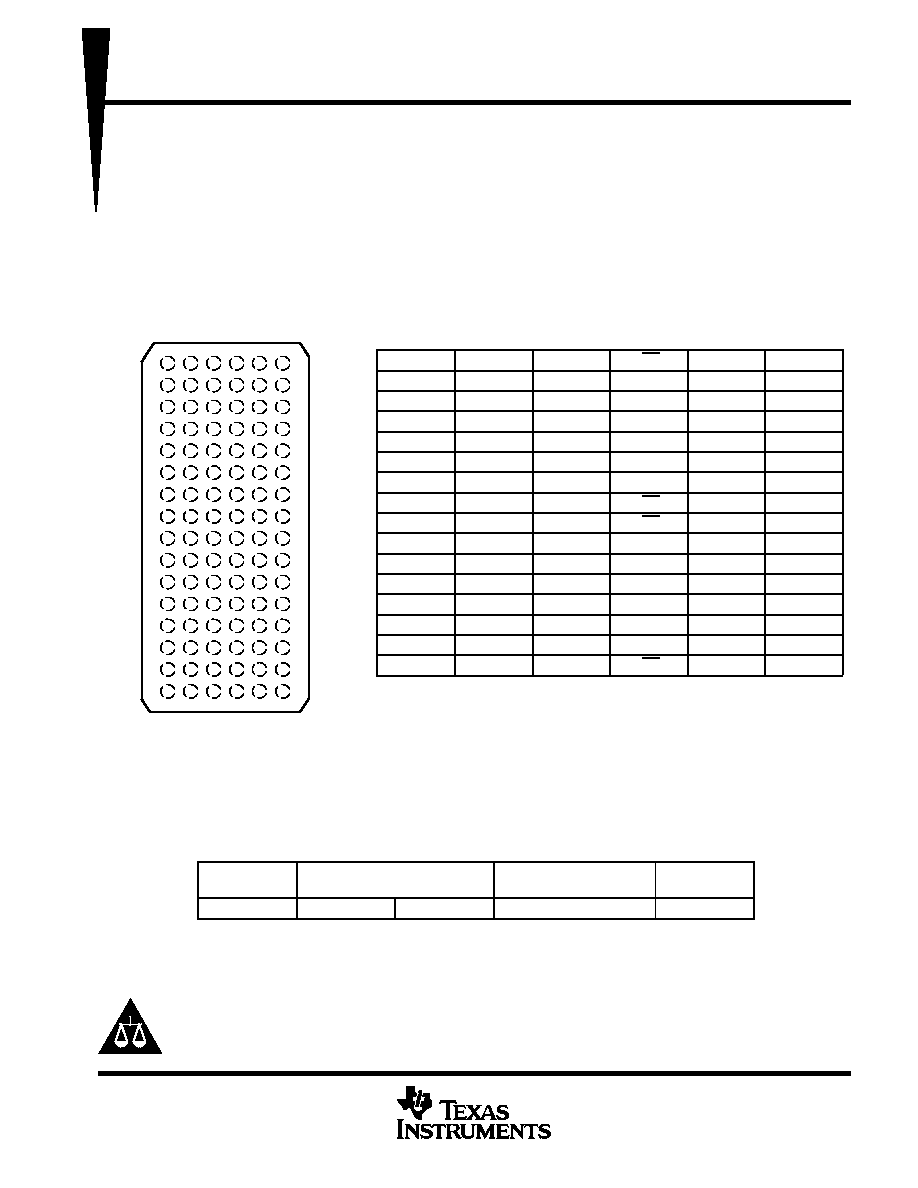
terminal assignments
1
2
3
4
5
6
A
1B2
1B1
1DIR
1OE
1A1
1A2
B
1B4
1B3
GND
GND
1A3
1A4
C
1B6
1B5
VCC
VCC
1A5
1A6
D
1B8
1B7
GND
GND
1A7
1A8
E
2B2
2B1
GND
GND
2A1
2A2
F
2B4
2B3
VCC
VCC
2A3
2A4
G
2B6
2B5
GND
GND
2A5
2A6
H
2B7
2B8
2DIR
2OE
2A8
2A7
J
3B2
3B1
3DIR
3OE
3A1
3A2
K
3B4
3B3
GND
GND
3A3
3A4
L
3B6
3B5
VCC
VCC
3A5
3A6
M
3B8
3B7
GND
GND
3A7
3A8
N
4B2
4B1
GND
GND
4A1
4A2
P
4B4
4B3
VCC
VCC
4A3
4A4
R
4B6
4B5
GND
GND
4A5
4A6
T
4B7
4B8
4DIR
4OE
4A8
4A7
description/ordering information
This 32-bit (quad-octal) noninverting bus transceiver is designed for 2.7-V to 3.6-V V
CC
operation.
The SN74LVCZ32245A is designed for asynchronous communication between data buses. The
control-function implementation minimizes external timing requirements.
ORDERING INFORMATION
TA
PACKAGE
ORDERABLE
PART NUMBER
TOP-SIDE
MARKING
40
°
C to 85
°
C
LFBGA GKE
Tape and reel
SN74LVCZ32245AGKER
ZC245A
Package drawings, standard packing quantities, thermal data, symbolization, and PCB design guidelines
are available at www.ti.com/sc/package.
Copyright
2003, Texas Instruments Incorporated
Please be aware that an important notice concerning availability, standard warranty, and use in critical applications of
Texas Instruments semiconductor products and disclaimers thereto appears at the end of this data sheet.
Widebus+ is a trademark of Texas Instruments.
PRODUCTION DATA information is current as of publication date.
Products conform to specifications per the terms of Texas Instruments
standard warranty. Production processing does not necessarily include
testing of all parameters.
GKE PACKAGE
(TOP VIEW)
1
2
3
4
5
6
A
B
C
D
E
F
G
H
J
K
L
M
N
P
R
T
SN74LVCZ32245A
32 BIT BUS TRANSCEIVER
WITH 3 STATE OUTPUTS
SCES423 JANUARY 2003
2
POST OFFICE BOX 655303
·
DALLAS, TEXAS 75265
description/ordering information (continued)
This device can be used as four 8-bit transceivers, two 16-bit transceivers, or one 32-bit transceiver. It allows
data transmission from the A bus to the B bus or from the B bus to the A bus, depending on the logic level at
the direction-control (DIR) input. The output-enable (OE) input can be used to disable the device so that the
buses are effectively isolated.
Inputs can be driven from either 3.3-V or 5-V devices. This feature allows the use of these devices as translators
in a mixed 3.3-V/5-V system environment.
When V
CC
is between 0 and 1.5 V, the device is in the high-impedance state during power up or power down.
However, to ensure the high-impedance state above 1.5 V, OE should be tied to V
CC
through a pullup resistor;
the minimum value of the resistor is determined by the current-sinking capability of the driver.
This device is fully specified for hot-insertion applications using I
off
and power-up 3-state. The I
off
circuitry
disables the outputs, preventing damaging current backflow through the device when it is powered down. The
power-up 3-state circuitry places the outputs in the high-impedance state during power up and power down,
which prevents driver conflict.
FUNCTION TABLE
(each 8-bit section)
INPUTS
OPERATION
OE
DIR
OPERATION
L
L
B data to A bus
L
H
A data to B bus
H
X
Isolation
SN74LVCZ32245A
32 BIT BUS TRANSCEIVER
WITH 3 STATE OUTPUTS
SCES423 JANUARY 2003
3
POST OFFICE BOX 655303
·
DALLAS, TEXAS 75265
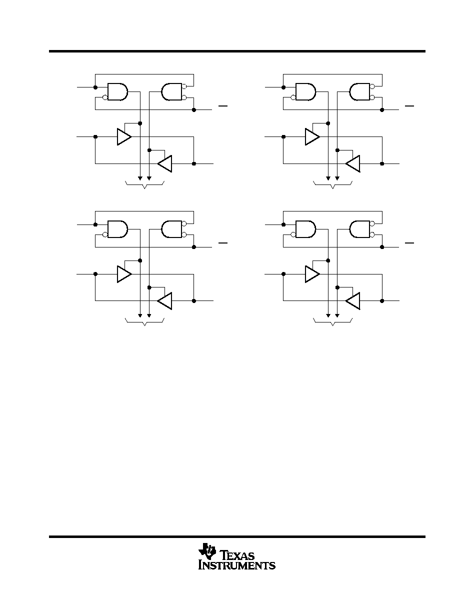
logic diagram (positive logic)
To Seven Other Channels
1DIR
1A1
1B1
1OE
To Seven Other Channels
2DIR
2A1
2B1
2OE
A3
A5
H3
E5
A4
A2
H4
E2
To Seven Other Channels
3DIR
3A1
3B1
3OE
To Seven Other Channels
4DIR
4A1
4B1
4OE
J3
J5
T3
N5
J4
J2
T4
N2
absolute maximum ratings over operating free-air temperature range (unless otherwise noted)
Supply voltage range, V
CC
0.5 V to 6.5 V
. . . . . . . . . . . . . . . . . . . . . . . . . . . . . . . . . . . . . . . . . . . . . . . . . . . . . . . . .
Input voltage range, V
I
(see Note 1)
0.5 V to 6.5 V
. . . . . . . . . . . . . . . . . . . . . . . . . . . . . . . . . . . . . . . . . . . . . . . . .
Voltage range applied to any output in the high-impedance or power-off state, V
O
(see Note 1)
0.5 V to 6.5 V
. . . . . . . . . . . . . . . . . . . . . . . . . . . . . . . . . . . . . . . . . . . . . . . . . . . . . . . . . . . . . . . . . . .
Voltage range applied to any output in the high or low state, V
O
(see Notes 1 and 2)
0.5 V to V
CC
+ 0.5 V
. . . . . . . . . . . . . . . . . . . . . . . . . . . . . . . . . . . . . . . . . . . . . . . . . . . . . . .
Input clamp current, I
IK
(V
I
< 0)
50 mA
. . . . . . . . . . . . . . . . . . . . . . . . . . . . . . . . . . . . . . . . . . . . . . . . . . . . . . . . . . .
Output clamp current, I
OK
(V
O
< 0)
50 mA
. . . . . . . . . . . . . . . . . . . . . . . . . . . . . . . . . . . . . . . . . . . . . . . . . . . . . . . .
Continuous output current, I
O
±
50 mA
. . . . . . . . . . . . . . . . . . . . . . . . . . . . . . . . . . . . . . . . . . . . . . . . . . . . . . . . . . . . .
Continuous current through each V
CC
or GND
±
100 mA
. . . . . . . . . . . . . . . . . . . . . . . . . . . . . . . . . . . . . . . . . . . . .
Package thermal impedance,
JA
(see Note 2)
40
°
C/W
. . . . . . . . . . . . . . . . . . . . . . . . . . . . . . . . . . . . . . . . . . . . .
Storage temperature range, T
stg
65
°
C to 150
°
C
. . . . . . . . . . . . . . . . . . . . . . . . . . . . . . . . . . . . . . . . . . . . . . . . . . .
Stresses beyond those listed under "absolute maximum ratings" may cause permanent damage to the device. These are stress ratings only, and
functional operation of the device at these or any other conditions beyond those indicated under "recommended operating conditions" is not
implied. Exposure to absolute-maximum-rated conditions for extended periods may affect device reliability.
NOTES:
1. The input negative-voltage and output voltage ratings may be exceeded if the input and output current ratings are observed.
2. The value of VCC is provided in the recommended operating conditions table.
3. The package thermal impedance is calculated in accordance with JESD 51-7.
SN74LVCZ32245A
32 BIT BUS TRANSCEIVER
WITH 3 STATE OUTPUTS
SCES423 JANUARY 2003
4
POST OFFICE BOX 655303
·
DALLAS, TEXAS 75265
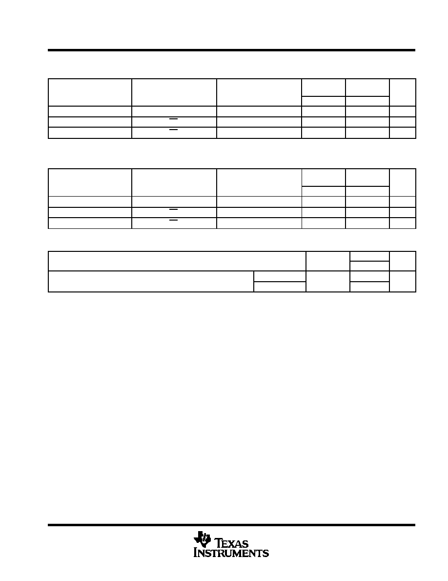
recommended operating conditions (see Note 4)
MIN
MAX
UNIT
VCC
Supply voltage
2.7
3.6
V
VIH
High-level input voltage
VCC = 2.7 V to 3.6 V
2
V
VIL
Low-level input voltage
VCC = 2.7 V to 3.6 V
0.8
V
VI
Input voltage
0
5.5
V
V
O tp t oltage
High or low state
0
VCC
V
VO
Output voltage
3-state
0
5.5
V
I
High le el o tp t c rrent
VCC = 2.7 V
12
mA
IOH
High-level output current
VCC = 3 V
24
mA
I
Lo
le el o tp t c rrent
VCC = 2.7 V
12
mA
IOL
Low-level output current
VCC = 3 V
24
mA
t/
v
Input transition rise or fall rate
6
ns/V
t/
VCC
Power-up ramp rate
150
µ
s/V
TA
Operating free-air temperature
40
85
°
C
NOTE 4: All unused inputs of the device must be held at VCC or GND to ensure proper device operation. Refer to the TI application report,
Implications of Slow or Floating CMOS Inputs, literature number SCBA004.
electrical characteristics over recommended operating free-air temperature range (unless
otherwise noted)
PARAMETER
TEST CONDITIONS
VCC
MIN
TYP
MAX
UNIT
IOH = 100
µ
A
2.7 V to 3.6 V
VCC0.2
V
I
12 mA
2.7 V
2.2
V
VOH
IOH = 12 mA
3 V
2.4
V
IOH = 24 mA
3 V
2.2
IOL = 100
µ
A
2.7 V to 3.6 V
0.2
VOL
IOL = 12 mA
2.7 V
0.4
V
VOL
IOL = 24 mA
3 V
0.55
V
II
Control inputs
VI = 0 to 5.5 V
3.6 V
±
5
µ
A
Ioff
VI or VO = 5.5 V
0
±
5
µ
A
IOZ
VO = 0 to 5.5 V
3.6 V
±
5
µ
A
IOZPU
VO = 0.5 V to 2.5 V,
OE = don't care
0 to 1.5 V
±
5
µ
A
IOZPD
VO = 0.5 V to 2.5 V,
OE = don't care
1.5 V to 0
±
5
µ
A
I
VI = VCC or GND
I
0
3 6 V
120
A
ICC
3.6 V
VI
5.5 V§
IO = 0
3.6 V
120
µ
A
ICC
One input at VCC 0.6 V, Other inputs at VCC or GND
2.7 V to 3.6 V
500
µ
A
Ci
Control inputs
VI = VCC or GND
3.3 V
5
pF
Cio
A or B ports
VO = VCC or GND
3.3 V
6.5
pF
All typical values are at VCC = 3.3 V, TA = 25
°
C.
For I/O ports, the parameter IOZ includes the input leakage current.
§ This applies in the disabled state only.
SN74LVCZ32245A
32 BIT BUS TRANSCEIVER
WITH 3 STATE OUTPUTS
SCES423 JANUARY 2003
5
POST OFFICE BOX 655303
·
DALLAS, TEXAS 75265
switching characteristics over recommended operating free-air temperature range, C
L
= 50 pF
(unless otherwise noted) (see Figure 1)
PARAMETER
FROM
(INPUT)
TO
(OUTPUT)
VCC = 2.7 V
VCC = 3.3 V
±
0.3 V
UNIT
PARAMETER
(INPUT)
(OUTPUT)
MIN
MAX
MIN
MAX
UNIT
tpd
A or B
B or A
4.2
1.3
4
ns
ten
OE
A or B
6.1
1.4
5.6
ns
tdis
OE
A or B
7.1
2
6.6
ns
switching characteristics over recommended operating free-air temperature range, C
L
= 30 pF
(unless otherwise noted) (see Figure 1)
PARAMETER
FROM
(INPUT)
TO
(OUTPUT)
VCC = 2.7 V
VCC = 3.3 V
±
0.3 V
UNIT
PARAMETER
(INPUT)
(OUTPUT)
MIN
MAX
MIN
MAX
UNIT
tpd
A or B
B or A
3.9
1
3.7
ns
ten
OE
A or B
5.9
1.1
5.4
ns
tdis
OE
A or B
6.7
1.6
6.2
ns
operating characteristics, T
A
= 25
°
C
PARAMETER
TEST
VCC = 3.3 V
UNIT
PARAMETER
TEST
CONDITIONS
TYP
UNIT
Cpd
Power dissipation capacitance per transceiver
Outputs enabled
f
10 MHz
42
pF
Cpd
Power dissipation capacitance per transceiver
Outputs disabled
f = 10 MHz
4
pF