
SN74LVC543A
OCTAL REGISTERED TRANSCEIVER
WITH 3 STATE OUTPUTS
SCAS299H - JANUARY 1993 - REVISED AUGUST 2003
1
POST OFFICE BOX 655303
·
DALLAS, TEXAS 75265
D
Operates From 1.65 V to 3.6 V
D
Inputs Accept Voltages to 5.5 V
D
Max t
pd
of 7 ns at 3.3 V
D
Typical V
OLP
(Output Ground Bounce)
<0.8 V at V
CC
= 3.3 V, T
A
= 25
°
C
D
Typical V
OHV
(Output V
OH
Undershoot)
>2 V at V
CC
= 3.3 V, T
A
= 25
°
C
D
Supports Mixed-Mode Signal Operation on
All Ports (5-V Input/Output Voltage With
3.3-V V
CC
)
D
I
off
Supports Partial-Power-Down Mode
Operation
D
Latch-Up Performance Exceeds 250 mA Per
JESD 17
description/ordering information
This octal registered transceiver is designed for 1.65-V to 3.6-V V
CC
operation.
The SN74LVC543A contains two sets of D-type latches for temporary storage of data flowing in either direction.
Separate latch-enable (LEAB or LEBA) and output-enable (OEAB or OEBA) inputs are provided for each
register to permit independent control in either direction of data flow.
The A-to-B enable (CEAB) input must be low to enter data from A or to output data from B. If CEAB is low and
LEAB is low, the A-to-B latches are transparent; a subsequent low-to-high transition of LEAB places the A
latches in the storage mode. With CEAB and OEAB both low, the 3-state B outputs are active and reflect the
data present at the output of the A latches. Data flow for B to A is similar to that of A to B, but uses CEBA, LEBA,
and OEBA.
This device is fully specified for partial-power-down applications using I
off
. The I
off
circuitry disables the outputs,
preventing damaging current backflow through the device when it is powered down.
To ensure the high-impedance state during power up or power down, OE should be tied to V
CC
through a pullup
resistor; the minimum value of the resistor is determined by the current-sinking capability of the driver.
Inputs can be driven from either 3.3-V or 5-V devices. This feature allows the use of these devices as translators
in a mixed 3.3-V/5-V system environment.
ORDERING INFORMATION
TA
PACKAGE
ORDERABLE
PART NUMBER
TOP-SIDE MARKING
SOIC - DW
Tube of 25
SN74LVC543ADW
LVC543A
SOIC - DW
Reel of 2000
SN74LVC543ADWR
LVC543A
-40
°
C to 85
°
C
SSOP - DB
Reel of 2000
SN74LVC543ADBR
LC543A
-40
°
C to 85
°
C
Tube of 60
SN74LVC543APW
TSSOP - PW
Reel of 2000
SN74LVC543APWR
LC543A
TSSOP - PW
Reel of 250
SN74LVC543APWT
LC543A
Package drawings, standard packing quantities, thermal data, symbolization, and PCB design guidelines are
available at www.ti.com/sc/package.
Copyright
2003, Texas Instruments Incorporated
PRODUCTION DATA information is current as of publication date.
Products conform to specifications per the terms of Texas Instruments
standard warranty. Production processing does not necessarily include
testing of all parameters.
Please be aware that an important notice concerning availability, standard warranty, and use in critical applications of
Texas Instruments semiconductor products and disclaimers thereto appears at the end of this data sheet.
DB, DW, OR PW PACKAGE
(TOP VIEW)
1
2
3
4
5
6
7
8
9
10
11
12
24
23
22
21
20
19
18
17
16
15
14
13
LEBA
OEBA
A1
A2
A3
A4
A5
A6
A7
A8
CEAB
GND
V
CC
CEBA
B1
B2
B3
B4
B5
B6
B7
B8
LEAB
OEAB

SN74LVC543A
OCTAL REGISTERED TRANSCEIVER
WITH 3 STATE OUTPUTS
SCAS299H - JANUARY 1993 - REVISED AUGUST 2003
2
POST OFFICE BOX 655303
·
DALLAS, TEXAS 75265
FUNCTION TABLE
INPUTS
OUTPUT
CEAB
LEAB
OEAB
A
OUTPUT
B
H
X
X
X
Z
X
X
H
X
Z
L
H
L
X
B0
L
L
L
L
L
L
L
L
H
H
A-to-B data flow is shown; B-to-A flow control is the
same, except that it uses CEBA, LEBA, and
OEBA.
Output level before the indicated steady-state
input conditions were established
logic diagram (positive logic)
OEBA
CEBA
LEBA
OEAB
CEAB
LEAB
A1
B1
To Seven Other Channels
2
23
1
13
11
14
3
22
C1
1D
C1
1D

SN74LVC543A
OCTAL REGISTERED TRANSCEIVER
WITH 3 STATE OUTPUTS
SCAS299H - JANUARY 1993 - REVISED AUGUST 2003
3
POST OFFICE BOX 655303
·
DALLAS, TEXAS 75265
absolute maximum ratings over operating free-air temperature range (unless otherwise noted)
Supply voltage range, V
CC
-0.5 V to 6.5 V
. . . . . . . . . . . . . . . . . . . . . . . . . . . . . . . . . . . . . . . . . . . . . . . . . . . . . . . . .
Input voltage range, V
I
: (see Note 1)
-0.5 V to 6.5 V
. . . . . . . . . . . . . . . . . . . . . . . . . . . . . . . . . . . . . . . . . . . . . . . .
Voltage range applied to any output in the high-impedance or power-off state, V
O
(see Note 1)
-0.5 V to 6.5 V
. . . . . . . . . . . . . . . . . . . . . . . . . . . . . . . . . . . . . . . . . . . . . . . . . . . . . . . . . . . . . . . . . . .
Voltage range applied to any output in the high or low state, V
O
(see Notes 1 and 2)
-0.5 V to V
CC
+ 0.5 V
. . . . . . . . . . . . . . . . . . . . . . . . . . . . . . . . . . . . . . . . . . . . . . . . . . . . . . .
Input clamp current, I
IK
(V
I
< 0)
-50 mA
. . . . . . . . . . . . . . . . . . . . . . . . . . . . . . . . . . . . . . . . . . . . . . . . . . . . . . . . . . .
Output clamp current, I
OK
(V
O
< 0)
-50 mA
. . . . . . . . . . . . . . . . . . . . . . . . . . . . . . . . . . . . . . . . . . . . . . . . . . . . . . . .
Continuous output current, I
O
±
50 mA
. . . . . . . . . . . . . . . . . . . . . . . . . . . . . . . . . . . . . . . . . . . . . . . . . . . . . . . . . . . . .
Continuous current through V
CC
or GND
±
100 mA
. . . . . . . . . . . . . . . . . . . . . . . . . . . . . . . . . . . . . . . . . . . . . . . . . .
Package thermal impedance,
JA
(see Note 3): DB package
63
°
C/W
. . . . . . . . . . . . . . . . . . . . . . . . . . . . . . . . .
DW package
46
°
C/W
. . . . . . . . . . . . . . . . . . . . . . . . . . . . . . . . .
PW package
88
°
C/W
. . . . . . . . . . . . . . . . . . . . . . . . . . . . . . . . .
Storage temperature range, T
stg
-65
°
C to 150
°
C
. . . . . . . . . . . . . . . . . . . . . . . . . . . . . . . . . . . . . . . . . . . . . . . . . . .
Stresses beyond those listed under "absolute maximum ratings" may cause permanent damage to the device. These are stress ratings only, and
functional operation of the device at these or any other conditions beyond those indicated under "recommended operating conditions" is not
implied. Exposure to absolute-maximum-rated conditions for extended periods may affect device reliability.
NOTES:
1. The input negative-voltage and output voltage ratings may be exceeded if the input and output current ratings are observed.
2. The value of VCC is provided in the recommended operating conditions table.
3. The package thermal impedance is calculated in accordance with JESD 51-7.
recommended operating conditions (see Note 4)
MIN
MAX
UNIT
VCC
Supply voltage
Operating
1.65
3.6
V
VCC
Supply voltage
Data retention only
1.5
V
VCC = 1.65 V to 1.95 V
0.65
×
VCC
VIH
High-level input voltage
VCC = 2.3 V to 2.7 V
1.7
V
VIH
High-level input voltage
VCC = 2.7 V to 3.6 V
2
V
VCC = 1.65 V to 1.95 V
0.35
×
VCC
VIL
Low-level input voltage
VCC = 2.3 V to 2.7 V
0.7
V
VIL
Low-level input voltage
VCC = 2.7 V to 3.6 V
0.8
V
VI
Input voltage
0
5.5
V
VO
Output voltage
High or low state
0
VCC
V
VO
Output voltage
3-state
0
5.5
V
VCC = 1.65 V
-4
IOH
High-level output current
VCC = 2.3 V
-8
mA
IOH
High-level output current
VCC = 2.7 V
-12
mA
VCC = 3 V
-24
VCC = 1.65 V
4
IOL
Low-level output current
VCC = 2.3 V
8
mA
IOL
Low-level output current
VCC = 2.7 V
12
mA
VCC = 3 V
24
t/
v
Input transition rise or fall rate
10
ns/V
TA
Operating free-air temperature
-40
85
°
C
NOTE 4: All unused inputs of the device must be held at VCC or GND to ensure proper device operation. Refer to the TI application report,
Implications of Slow or Floating CMOS Inputs, literature number SCBA004.
SN74LVC543A
OCTAL REGISTERED TRANSCEIVER
WITH 3 STATE OUTPUTS
SCAS299H - JANUARY 1993 - REVISED AUGUST 2003
4
POST OFFICE BOX 655303
·
DALLAS, TEXAS 75265
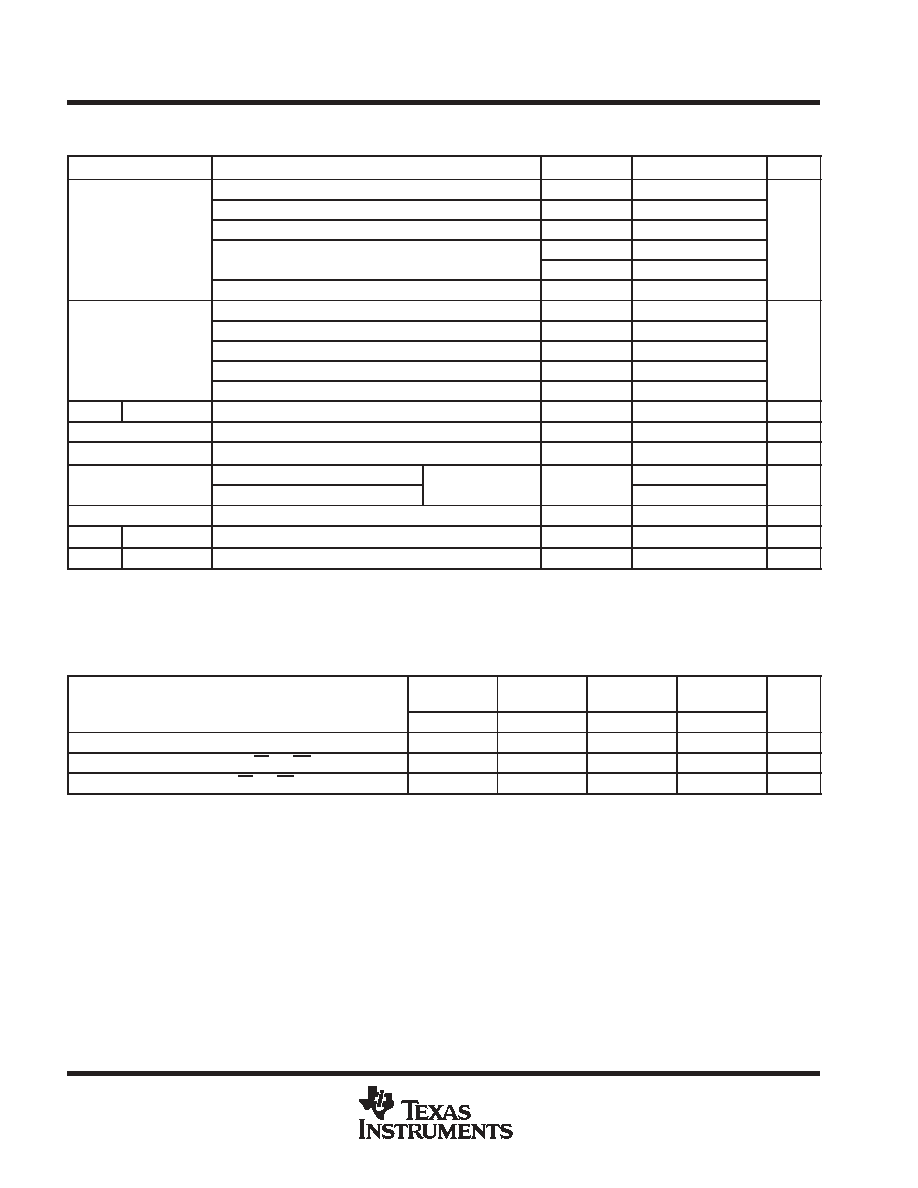
electrical characteristics over recommended operating free-air temperature range (unless
otherwise noted)
PARAMETER
TEST CONDITIONS
VCC
MIN
TYP
MAX
UNIT
IOH = -100
µ
A
1.65 V to 3.6 V
VCC-0.2
IOH = -4 mA
1.65 V
1.2
VOH
IOH = -8 mA
2.3 V
1.7
V
VOH
IOH = -12 mA
2.7 V
2.2
V
IOH = -12 mA
3 V
2.4
IOH = -24 mA
3 V
2.2
IOL = 100
µ
A
1.65 V to 3.6 V
0.2
IOL = 4 mA
1.65 V
0.45
VOL
IOL = 8 mA
2.3 V
0.7
V
VOL
IOL = 12 mA
2.7 V
0.4
V
IOL = 24 mA
3 V
0.55
II
Control inputs
VI = 0 to 5.5 V
3.6 V
±
5
µ
A
Ioff
VI or VO = 5.5 V
0
±
10
µ
A
IOZ
VO = 0 to 5.5 V
3.6 V
±
10
µ
A
ICC
VI = VCC or GND
IO = 0
3.6 V
10
A
ICC
3.6 V
VI
5.5 V§
IO = 0
3.6 V
10
µ
A
ICC
One input at VCC - 0.6 V, Other inputs at VCC or GND
2.7 V to 3.6 V
500
µ
A
Ci
Control inputs
VI = VCC or GND
3.3 V
4.5
pF
Cio
A or B ports
VO = VCC or GND
3.3 V
7.5
pF
All typical values are at VCC = 3.3 V, TA = 25
°
C.
For I/O ports, the parameter IOZ includes the input leakage current.
§ This applies in the disabled state only.
timing requirements over recommended operating free-air temperature range (unless otherwise
noted) (see Figure 1)
VCC = 1.8 V
±
0.15 V
VCC = 2.5 V
±
0.2 V
VCC = 2.7 V
VCC = 3.3 V
±
0.3 V
UNIT
MIN
MAX
MIN
MAX
MIN
MAX
MIN
MAX
UNIT
tw
Pulse duration
¶
¶
3.3
3.3
ns
tsu
Setup time, data before LE
or CE
¶
¶
1.6
1.6
ns
th
Hold time, data after LE
or CE
¶
¶
2.1
2.1
ns
¶ This information was not available at the time of publication.

SN74LVC543A
OCTAL REGISTERED TRANSCEIVER
WITH 3 STATE OUTPUTS
SCAS299H - JANUARY 1993 - REVISED AUGUST 2003
5
POST OFFICE BOX 655303
·
DALLAS, TEXAS 75265
switching characteristics over recommended operating free-air temperature range (unless
otherwise noted) (see Figure 1)
PARAMETER
FROM
(INPUT)
TO
(OUTPUT)
VCC = 1.8 V
±
0.15 V
VCC = 2.5 V
±
0.2 V
VCC = 2.7 V
VCC = 3.3 V
±
0.3 V
UNIT
PARAMETER
(INPUT)
(OUTPUT)
MIN
MAX
MIN
MAX
MIN
MAX
MIN
MAX
UNIT
tpd
A or B
B or A
8
1
7
ns
tpd
LE
B or A
9.5
1.2
8.5
ns
ten
OE
A or B
9.2
1.3
7.7
ns
ten
CE
A or B
9.3
1.3
8
ns
tdis
OE
A or B
7.5
1
7
ns
tdis
CE
A or B
7.5
1
7
ns
This information was not available at the time of publication.
operating characteristics, T
A
= 25
°
C
PARAMETER
TEST
VCC = 1.8 V
VCC = 2.5 V
VCC = 3.3 V
UNIT
PARAMETER
TEST
CONDITIONS
TYP
TYP
TYP
UNIT
Cpd
Power dissipation capacitance
Outputs enabled
f = 10 MHz
49
pF
Cpd
Power dissipation capacitance
per transceiver
Outputs disabled
f = 10 MHz
6
pF
This information was not available at the time of publication.