SN54LVC00A, SN74LVC00A
QUADRUPLE 2-INPUT POSITIVE-NAND GATES
SCAS279G JANUARY 1993 REVISED JUNE 1998
1
POST OFFICE BOX 655303
·
DALLAS, TEXAS 75265
D
EPIC
TM
(Enhanced-Performance Implanted
CMOS) Submicron Process
D
ESD Protection Exceeds 2000 V Per
MIL-STD-883, Method 3015; Exceeds 200 V
Using Machine Model (C = 200 pF, R = 0)
D
Latch-Up Performance Exceeds 250 mA Per
JESD 17
D
Typical V
OLP
(Output Ground Bounce)
< 0.8 V at V
CC
= 3.3 V, T
A
= 25
°
C
D
Typical V
OHV
(Output V
OH
Undershoot)
> 2 V at V
CC
= 3.3 V, T
A
= 25
°
C
D
Inputs Accept Voltages to 5.5 V
D
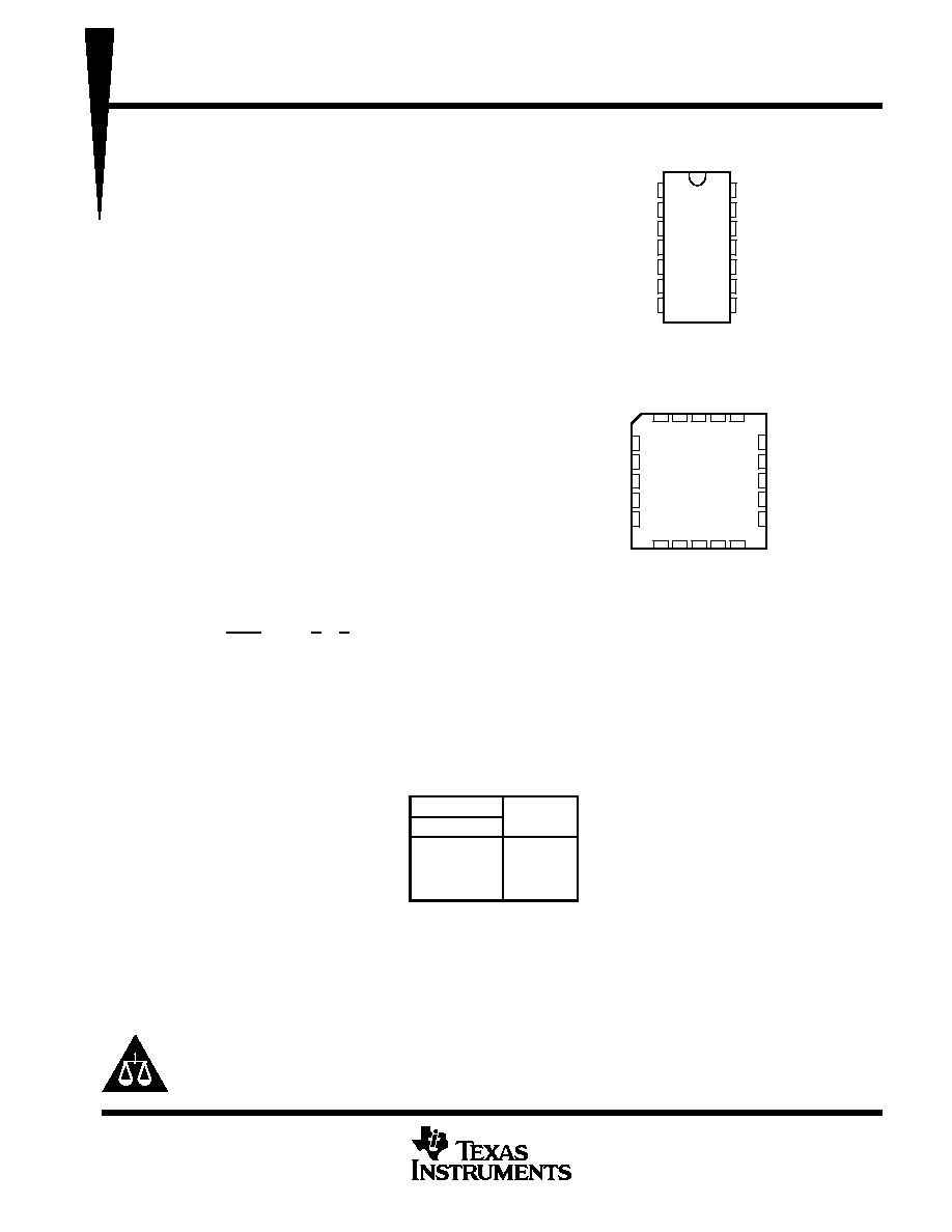
Package Options Include Plastic
Small-Outline (D), Shrink Small-Outline
(DB), and Thin Shrink Small-Outline (PW)
Packages, Ceramic Chip Carriers (FK),
Ceramic Flat (W) Package, and DIPs (J)
description
The SN54LVC00A quadruple 2-input positive-
NAND gate is designed for 2.7-V to 3.6-V V
CC
operation and the SN74LVC00A quadruple
2-input positive-NAND gate is designed for 1.65-V
to 3.6-V V
CC
operation.
The 'LVC00A devices perform the Boolean
function Y = A
·
B or Y = A + B in positive logic.
Inputs can be driven from either 3.3-V or 5-V devices. This feature allows the use of these devices as translators
in a mixed 3.3-V/5-V system environment.
The SN54LVC00A is characterized for operation over the full military temperature range of 55
°
C to 125
°
C. The
SN74LVC00A is characterized for operation from 40
°
C to 85
°
C.
FUNCTION TABLE
(each gate)
INPUTS
OUTPUT
A
B
Y
H
H
L
L
X
H
X
L
H
Copyright
©
1998, Texas Instruments Incorporated
PRODUCTION DATA information is current as of publication date.
Products conform to specifications per the terms of Texas Instruments
standard warranty. Production processing does not necessarily include
testing of all parameters.
Please be aware that an important notice concerning availability, standard warranty, and use in critical applications of
Texas Instruments semiconductor products and disclaimers thereto appears at the end of this data sheet.
EPIC is a trademark of Texas Instruments Incorporated.
1
2
3
4
5
6
7
14
13
12
11
10
9
8
1A
1B
1Y
2A
2B
2Y
GND
V
CC
4B
4A
4Y
3B
3A
3Y
SN54LVC00A . . . J OR W PACKAGE
SN74LVC00A . . . D, DB, OR PW PACKAGE
(TOP VIEW)
3
2 1 20 19
9 10 11 12 13
4
5
6
7
8
18
17
16
15
14
4A
NC
4Y
NC
3B
1Y
NC
2A
NC
2B
1B
1A
NC
3Y
3A
V
4B
2Y
GND
NC
SN54LVC00A . . . FK PACKAGE
(TOP VIEW)
CC
NC No internal connection
On products compliant to MIL-PRF-38535, all parameters are tested
unless otherwise noted. On all other products, production
processing does not necessarily include testing of all parameters.

SN54LVC00A, SN74LVC00A
QUADRUPLE 2-INPUT POSITIVE-NAND GATES
SCAS279G JANUARY 1993 REVISED JUNE 1998
2
POST OFFICE BOX 655303
·
DALLAS, TEXAS 75265
logic symbol
1
1A
2
1B
1Y
3
4
2A
5
2B
2Y
6
9
3A
10
3B
3Y
8
12
4A
13
4B
4Y
11
&
This symbol is in accordance with ANSI/IEEE Std 91-1984 and IEC Publication 617-12.
Pin numbers shown are for the D, DB, J, PW, and W packages.
logic diagram, each gate (positive logic)
A
B
Y
absolute maximum ratings over operating free-air temperature range (unless otherwise noted)
Supply voltage range, V
CC
0.5 V to 6.5 V
. . . . . . . . . . . . . . . . . . . . . . . . . . . . . . . . . . . . . . . . . . . . . . . . . . . . . . . . .
Input voltage range, V
I
(see Note 1)
0.5 V to 6.5 V
. . . . . . . . . . . . . . . . . . . . . . . . . . . . . . . . . . . . . . . . . . . . . . . . .
Output voltage range, V
O
(see Notes 1 and 2)
0.5 V to V
CC
+ 0.5 V
. . . . . . . . . . . . . . . . . . . . . . . . . . . . . . . . . .
Input clamp current, I
IK
(V
I
< 0)
50 mA
. . . . . . . . . . . . . . . . . . . . . . . . . . . . . . . . . . . . . . . . . . . . . . . . . . . . . . . . . . .
Output clamp current, I
OK
(V
O
< 0)
50 mA
. . . . . . . . . . . . . . . . . . . . . . . . . . . . . . . . . . . . . . . . . . . . . . . . . . . . . . . .
Continuous output current, I
O
±
50 mA
. . . . . . . . . . . . . . . . . . . . . . . . . . . . . . . . . . . . . . . . . . . . . . . . . . . . . . . . . . . . .
Continuous current through V
CC
or GND
±
100 mA
. . . . . . . . . . . . . . . . . . . . . . . . . . . . . . . . . . . . . . . . . . . . . . . . . .
Package thermal impedance,
JA
(see Note 3): D package
127
°
C/W
. . . . . . . . . . . . . . . . . . . . . . . . . . . . . . . . . .
DB package
158
°
C/W
. . . . . . . . . . . . . . . . . . . . . . . . . . . . . . . .
PW package
170
°
C/W
. . . . . . . . . . . . . . . . . . . . . . . . . . . . . . . .
Storage temperature range, T
stg
65
°
C to 150
°
C
. . . . . . . . . . . . . . . . . . . . . . . . . . . . . . . . . . . . . . . . . . . . . . . . . . .
Stresses beyond those listed under "absolute maximum ratings" may cause permanent damage to the device. These are stress ratings only, and
functional operation of the device at these or any other conditions beyond those indicated under "recommended operating conditions" is not
implied. Exposure to absolute-maximum-rated conditions for extended periods may affect device reliability.
NOTES:
1. The input negative-voltage and output voltage ratings may be exceeded if the input and output current ratings are observed.
2. The value of VCC is provided in the recommended operating conditions table.
3. The package thermal impedance is calculated in accordance with JESD 51.
SN54LVC00A, SN74LVC00A
QUADRUPLE 2-INPUT POSITIVE-NAND GATES
SCAS279G JANUARY 1993 REVISED JUNE 1998
3
POST OFFICE BOX 655303
·
DALLAS, TEXAS 75265
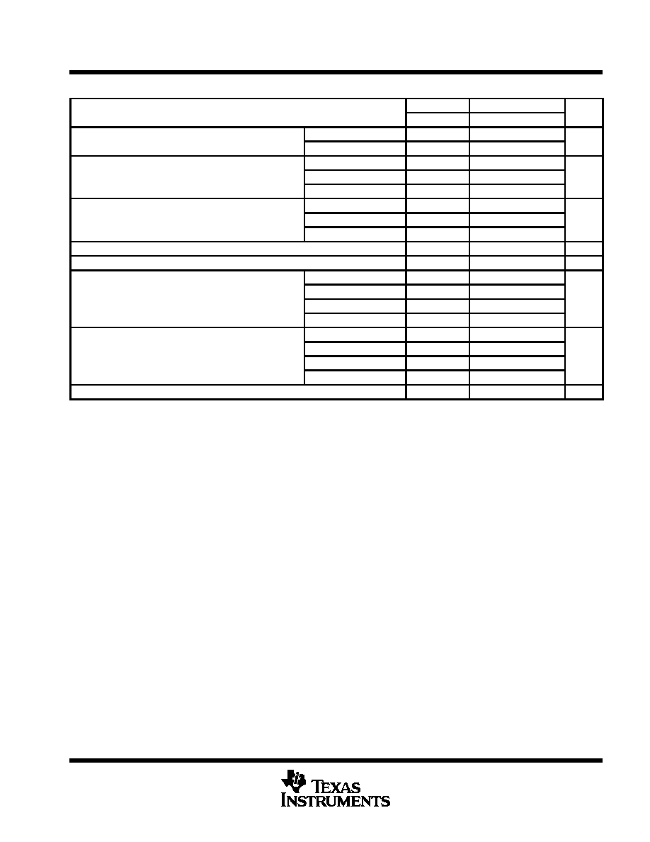
recommended operating conditions (see Note 4)
SN54LVC00A
SN74LVC00A
UNIT
MIN
MAX
MIN
MAX
UNIT
VCC
Supply voltage
Operating
2
3.6
1.65
3.6
V
VCC
Supply voltage
Data retention only
1.5
1.5
V
VCC = 1.65 V to 1.95 V
0.65
×
VCC
VIH
High-level input voltage
VCC = 2.3 V to 2.7 V
1.7
V
VCC = 2.7 V to 3.6 V
2
2
VCC = 1.65 V to 1.95 V
0.35
×
VCC
VIL
Low-level input voltage
VCC = 2.3 V to 2.7 V
0.7
V
VCC = 2.7 V to 3.6 V
0.8
0.8
VI
Input voltage
0
5.5
0
5.5
V
VO
Output voltage
0
VCC
0
VCC
V
VCC = 1.65 V
4
IOH
High level output current
VCC = 2.3 V
8
mA
IOH
High-level output current
VCC = 2.7 V
12
12
mA
VCC = 3 V
24
24
VCC = 1.65 V
4
IOL
Low level output current
VCC = 2.3 V
8
mA
IOL
Low-level output current
VCC = 2.7 V
12
12
mA
VCC = 3 V
24
24
TA
Operating free-air temperature
55
125
40
85
°
C
NOTE 4: All unused inputs of the device must be held at VCC or GND to ensure proper device operation. Refer to the TI application report,
Implications of Slow or Floating CMOS Inputs, literature number SCBA004.
SN54LVC00A, SN74LVC00A
QUADRUPLE 2-INPUT POSITIVE-NAND GATES
SCAS279G JANUARY 1993 REVISED JUNE 1998
4
POST OFFICE BOX 655303
·
DALLAS, TEXAS 75265
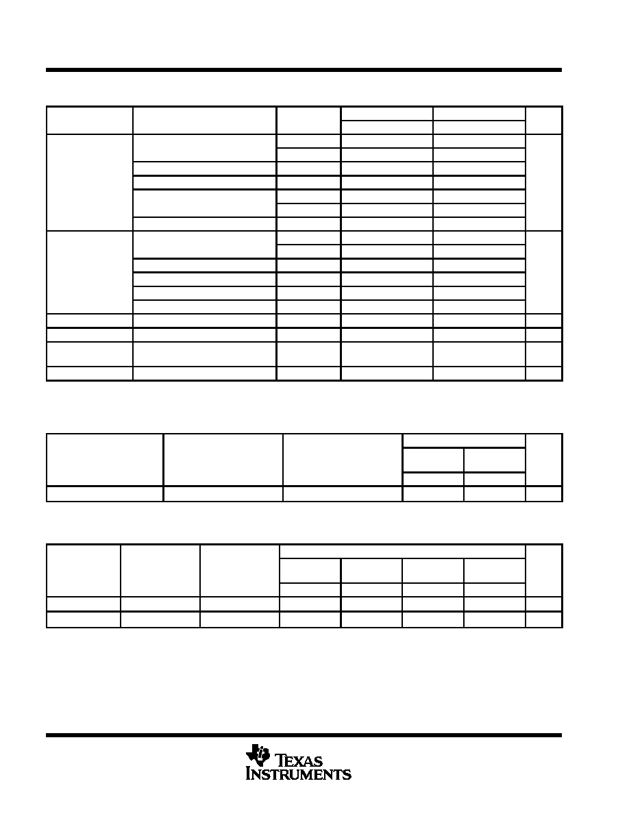
electrical characteristics over recommended operating free-air temperature range (unless
otherwise noted)
PARAMETER
TEST CONDITIONS
V
SN54LVC00A
SN74LVC00A
UNIT
PARAMETER
TEST CONDITIONS
VCC
MIN
TYP
MAX
MIN
TYP
MAX
UNIT
IOH = 100
µ
A
1.65 V to 3.6 V
VCC0.2
IOH = 100
µ
A
2.7 V to 3.6 V
VCC0.2
IOH = 4 mA
1.65 V
1.2
VOH
IOH = 8 mA
2.3 V
1.7
V
IOH = 12 mA
2.7 V
2.2
2.2
IOH = 12 mA
3 V
2.4
2.4
IOH = 24 mA
3 V
2.2
2.2
IOL = 100
µ
A
1.65 V to 3.6 V
0.2
IOL = 100
µ
A
2.7 V to 3.6 V
0.2
VOL
IOL = 4 mA
1.65 V
0.45
V
VOL
IOL = 8 mA
2.3 V
0.7
V
IOL = 12 mA
2.7 V
0.4
0.4
IOL = 24 mA
3 V
0.55
0.55
II
VI = 5.5 V or GND
3.6 V
±
5
±
5
µ
A
ICC
VI = VCC or GND,
IO = 0
3.6 V
10
10
µ
A
ICC
One input at VCC 0.6 V,
Other inputs at VCC or GND
2.7 V to 3.6 V
500
500
µ
A
Ci
VI = VCC or GND
3.3 V
5
5
pF
All typical values are at VCC = 3.3 V, TA = 25
°
C.
switching characteristics over recommended operating free-air temperature range (unless
otherwise noted) (see Figure 3)
SN54LVC00A
PARAMETER
FROM
(INPUT)
TO
(OUTPUT)
VCC = 2.7 V
VCC = 3.3 V
±
0.3 V
UNIT
MIN
MAX
MIN
MAX
tpd
A or B
Y
5.1
1
4.3
ns
switching characteristics over recommended operating free-air temperature range (unless
otherwise noted) (see Figures 1 through 3)
SN74LVC00A
PARAMETER
FROM
(INPUT)
TO
(OUTPUT)
VCC = 1.8 V
±
0.15 V
VCC = 2.5 V
±
0.2 V
VCC = 2.7 V
VCC = 3.3 V
±
0.3 V
UNIT
MIN
MAX
MIN
MAX
MIN
MAX
MIN
MAX
tpd
A or B
Y
5.1
1
4.3
ns
tsk(o)§
1
ns
This information was not available at the time of publication.
§ Skew between any two outputs of the same package switching in the same direction
SN54LVC00A, SN74LVC00A
QUADRUPLE 2-INPUT POSITIVE-NAND GATES
SCAS279G JANUARY 1993 REVISED JUNE 1998
5
POST OFFICE BOX 655303
·
DALLAS, TEXAS 75265
operating characteristics, T
A
= 25
°
C
PARAMETER
TEST
CONDITIONS
VCC = 1.8 V
±
0.15 V
VCC = 2.5 V
±
0.2 V
VCC = 3.3 V
±
0.3 V
UNIT
CONDITIONS
TYP
TYP
TYP
Cpd
Power dissipation capacitance per gate
f = 10 MHz
9.5
pF
This information was not available at the time of publication.
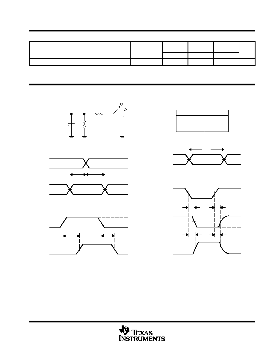
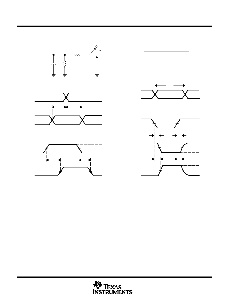
PARAMETER MEASUREMENT INFORMATION
V
CC
= 1.8 V
±
0.15 V
VCC/2
VCC/2
VCC/2
VCC/2
VCC/2
VCC/2
VCC/2
VCC/2
VOH
VOL
th
tsu
From Output
Under Test
CL = 30 pF
(see Note A)
LOAD CIRCUIT
S1
Open
GND
1k
1k
Output
Control
(low-level
enabling)
Output
Waveform 1
S1 at 2
×
VCC
(see Note B)
Output
Waveform 2
S1 at Open
(see Note B)
tPZL
tPZH
tPLZ
tPHZ
0 V
VOL + 0.15 V
VOH 0.15 V
0 V
VCC
0 V
0 V
tw
VCC
VCC
VOLTAGE WAVEFORMS
SETUP AND HOLD TIMES
VOLTAGE WAVEFORMS
PULSE DURATION
VOLTAGE WAVEFORMS
ENABLE AND DISABLE TIMES
Timing
Input
Data
Input
Input
tpd
tPLZ/tPZL
tPHZ/tPZH
Open
2
×
VCC
Open
TEST
S1
NOTES: A. CL includes probe and jig capacitance.
B. Waveform 1 is for an output with internal conditions such that the output is low except when disabled by the output control.
Waveform 2 is for an output with internal conditions such that the output is high except when disabled by the output control.
C. All input pulses are supplied by generators having the following characteristics: PRR
10 MHz, ZO = 50
, tr
2 ns, tf
2 ns.
D. The outputs are measured one at a time with one transition per measurement.
E. tPLZ and tPHZ are the same as tdis.
F. tPZL and tPZH are the same as ten.
G. tPLH and tPHL are the same as tpd.
0 V
VCC
VCC/2
tPHL
VCC/2
VCC/2
VCC
0 V
VOH
VOL
Input
Output
VOLTAGE WAVEFORMS
PROPAGATION DELAY TIMES
VCC/2
VCC/2
tPLH
2
×
VCC
VCC
Figure 1. Load Circuit and Voltage Waveforms
SN54LVC00A, SN74LVC00A
QUADRUPLE 2-INPUT POSITIVE-NAND GATES
SCAS279G JANUARY 1993 REVISED JUNE 1998
6
POST OFFICE BOX 655303
·
DALLAS, TEXAS 75265
PARAMETER MEASUREMENT INFORMATION
V
CC
= 2.5 V
±
0.2 V
VCC/2
VCC/2
VCC/2
VCC/2
VCC/2
VCC/2
VCC/2
VCC/2
VOH
VOL
th
tsu
From Output
Under Test
CL = 30 pF
(see Note A)
LOAD CIRCUIT
S1
Open
GND
500
500
Output
Control
(low-level
enabling)
Output
Waveform 1
S1 at 2
×
VCC
(see Note B)
Output
Waveform 2
S1 at GND
(see Note B)
tPZL
tPZH
tPLZ
tPHZ
0 V
VOL + 0.15 V
VOH 0.15 V
0 V
VCC
0 V
0 V
tw
VCC
VCC
VOLTAGE WAVEFORMS
SETUP AND HOLD TIMES
VOLTAGE WAVEFORMS
PULSE DURATION
VOLTAGE WAVEFORMS
ENABLE AND DISABLE TIMES
Timing
Input
Data
Input
Input
tpd
tPLZ/tPZL
tPHZ/tPZH
Open
2
×
VCC
GND
TEST
S1
NOTES: A. CL includes probe and jig capacitance.
B. Waveform 1 is for an output with internal conditions such that the output is low except when disabled by the output control.
Waveform 2 is for an output with internal conditions such that the output is high except when disabled by the output control.
C. All input pulses are supplied by generators having the following characteristics: PRR
10 MHz, ZO = 50
, tr
2 ns, tf
2 ns.
D. The outputs are measured one at a time with one transition per measurement.
E. tPLZ and tPHZ are the same as tdis.
F. tPZL and tPZH are the same as ten.
G. tPLH and tPHL are the same as tpd.
0 V
VCC
VCC/2
tPHL
VCC/2
VCC/2
VCC
0 V
VOH
VOL
Input
Output
VOLTAGE WAVEFORMS
PROPAGATION DELAY TIMES
VCC/2
VCC/2
tPLH
2
×
VCC
VCC
Figure 2. Load Circuit and Voltage Waveforms

SN54LVC00A, SN74LVC00A
QUADRUPLE 2-INPUT POSITIVE-NAND GATES
SCAS279G JANUARY 1993 REVISED JUNE 1998
7
POST OFFICE BOX 655303
·
DALLAS, TEXAS 75265
PARAMETER MEASUREMENT INFORMATION
V
CC
= 2.7 V AND 3.3 V
±
0.3 V
VOH
VOL
th
tsu
From Output
Under Test
CL = 50 pF
(see Note A)
LOAD CIRCUIT
S1
6 V
Open
GND
500
500
tPLH
tPHL
Output
Control
(low-level
enabling)
Output
Waveform 1
S1 at 6 V
(see Note B)
Output
Waveform 2
S1 at GND
(see Note B)
tPZL
tPZH
tPLZ
tPHZ
1.5 V
1.5 V
1.5 V
1.5 V
2.7 V
0 V
1.5 V
1.5 V
VOH
VOL
0 V
1.5 V
VOL + 0.3 V
1.5 V
VOH 0.3 V
0 V
1.5 V
2.7 V
0 V
1.5 V
1.5 V
0 V
2.7 V
0 V
1.5 V
1.5 V
tw
Input
2.7 V
2.7 V
3 V
VOLTAGE WAVEFORMS
SETUP AND HOLD TIMES
VOLTAGE WAVEFORMS
PROPAGATION DELAY TIMES
VOLTAGE WAVEFORMS
PULSE DURATION
VOLTAGE WAVEFORMS
ENABLE AND DISABLE TIMES
Timing
Input
Data
Input
Output
Input
tpd
tPLZ/tPZL
tPHZ/tPZH
Open
6 V
GND
TEST
S1
NOTES: A. CL includes probe and jig capacitance.
B. Waveform 1 is for an output with internal conditions such that the output is low except when disabled by the output control.
Waveform 2 is for an output with internal conditions such that the output is high except when disabled by the output control.
C. All input pulses are supplied by generators having the following characteristics: PRR
10 MHz, ZO = 50
, tr
2.5 ns, tf
2.5 ns.
D. The outputs are measured one at a time with one transition per measurement.
E. tPLZ and tPHZ are the same as tdis.
F. tPZL and tPZH are the same as ten.
G. tPLH and tPHL are the same as tpd.
Figure 3. Load Circuit and Voltage Waveforms

IMPORTANT NOTICE
Texas Instruments and its subsidiaries (TI) reserve the right to make changes to their products or to discontinue
any product or service without notice, and advise customers to obtain the latest version of relevant information
to verify, before placing orders, that information being relied on is current and complete. All products are sold
subject to the terms and conditions of sale supplied at the time of order acknowledgement, including those
pertaining to warranty, patent infringement, and limitation of liability.
TI warrants performance of its semiconductor products to the specifications applicable at the time of sale in
accordance with TI's standard warranty. Testing and other quality control techniques are utilized to the extent
TI deems necessary to support this warranty. Specific testing of all parameters of each device is not necessarily
performed, except those mandated by government requirements.
CERTAIN APPLICATIONS USING SEMICONDUCTOR PRODUCTS MAY INVOLVE POTENTIAL RISKS OF
DEATH, PERSONAL INJURY, OR SEVERE PROPERTY OR ENVIRONMENTAL DAMAGE ("CRITICAL
APPLICATIONS"). TI SEMICONDUCTOR PRODUCTS ARE NOT DESIGNED, AUTHORIZED, OR
WARRANTED TO BE SUITABLE FOR USE IN LIFE-SUPPORT DEVICES OR SYSTEMS OR OTHER
CRITICAL APPLICATIONS. INCLUSION OF TI PRODUCTS IN SUCH APPLICATIONS IS UNDERSTOOD TO
BE FULLY AT THE CUSTOMER'S RISK.
In order to minimize risks associated with the customer's applications, adequate design and operating
safeguards must be provided by the customer to minimize inherent or procedural hazards.
TI assumes no liability for applications assistance or customer product design. TI does not warrant or represent
that any license, either express or implied, is granted under any patent right, copyright, mask work right, or other
intellectual property right of TI covering or relating to any combination, machine, or process in which such
semiconductor products or services might be or are used. TI's publication of information regarding any third
party's products or services does not constitute TI's approval, warranty or endorsement thereof.
Copyright
©
1998, Texas Instruments Incorporated