SN54LV245, SN74LV245
OCTAL BUS TRANSCEIVERS
WITH 3-STATE OUTPUTS
SCLS075E ¡ JANUARY 1991 ¡ REVISED APRIL 1996
1
POST OFFICE BOX 655303
À
DALLAS, TEXAS 75265
D
EPIC
TM
(Enhanced-Performance Implanted
CMOS) 2-
Á
Process
D
Typical V
OLP
(Output Ground Bounce)
< 0.8 V at V
CC
, T
A
= 25
░
C
D
Typical V
OHV
(Output V
OH
Undershoot)
> 2 V at V
CC
, T
A
= 25
░
C
D
ESD Protection Exceeds 2000 V Per
MIL-STD-883C, Method 3015; Exceeds
200 V Using Machine Model
(C = 200 pF, R = 0)
D
Latch-Up Performance Exceeds 250 mA
Per JEDEC Standard JESD-17
D
Package Options Include Plastic
Small-Outline (DW), Shrink Small-Outline
(DB), Thin Shrink Small-Outline (PW),
Ceramic Flat (W) Packages, Chip Carriers
(FK), and (J) 300-mil DIPs
description
These octal bus transceivers are designed for
2.7-V to 5.5-V V
CC
operation.
The 'LV245 are designed for asynchronous
communication between data buses. The device
transmits data from the A bus to the B bus or from
the B bus to the A bus, depending upon the logic
level at the direction-control (DIR) input. The
output-enable (OE) input can be used to disable
the device so the buses are effectively isolated.
The SN74LV245 is available in TI's shrink small-outline package (DB), which provides the same I/O pin count
and functionality of standard small-outline packages in less than half the printed-circuit-board area.
The SN54LV245 is characterized for operation over the full military temperature range of ¡55
░
C to 125
░
C. The
SN74LV245 is characterized for operation from ¡40
░
C to 85
░
C.
FUNCTION TABLE
INPUTS
OPERATION
OE
DIR
OPERATION
L
L
B data to A bus
L
H
A data to B bus
H
X
Isolation
Copyright
®
1996, Texas Instruments Incorporated
UNLESS OTHERWISE NOTED this document contains PRODUCTION
DATA information current as of publication date. Products conform to
specifications per the terms of Texas Instruments standard warranty.
Production processing does not necessarily include testing of all
parameters.
EPIC is a trademark of Texas Instruments Incorporated.
Please be aware that an important notice concerning availability, standard warranty, and use in critical applications of
Texas Instruments semiconductor products and disclaimers thereto appears at the end of this data sheet.
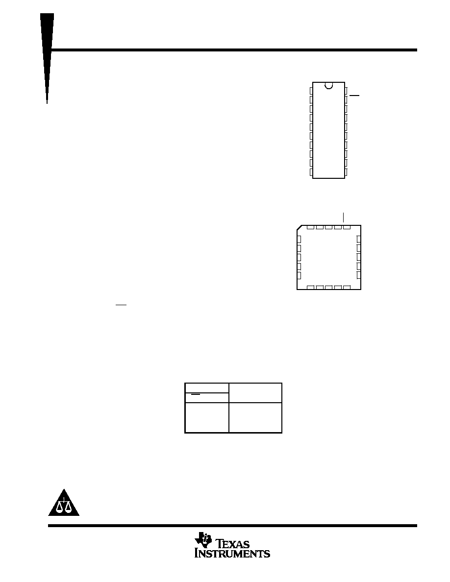
3
2
1 20 19
9 10 11 12 13
4
5
6
7
8
18
17
16
15
14
B1
B2
B3
B4
B5
A3
A4
A5
A6
A7
A2
A1
DIR
B7
B6
OE
A8
GND
B8
V
CC
SN54LV245 . . . FK PACKAGE
(TOP VIEW)
1
2
3
4
5
6
7
8
9
10
20
19
18
17
16
15
14
13
12
11
DIR
A1
A2
A3
A4
A5
A6
A7
A8
GND
V
CC
OE
B1
B2
B3
B4
B5
B6
B7
B8
SN54LV245 . . . J OR W PACKAGE
SN74LV245 . . . DB, DW, OR PW PACKAGE
(TOP VIEW)

SN54LV245, SN74LV245
OCTAL BUS TRANSCEIVERS
WITH 3-STATE OUTPUTS
SCLS075E ¡ JANUARY 1991 ¡ REVISED APRIL 1996
2
POST OFFICE BOX 655303
À
DALLAS, TEXAS 75265
logic symbol
logic diagram (positive logic)
A5
6
A6
7
A7
8
A8
9
A2
3
A3
4
A4
5
OE
A1
2
G3
19
3EN2[AB]
B5
14
B6
13
B7
12
B8
11
B1
18
B2
17
B3
16
B4
15
3EN1[BA]
1
DIR
DIR
OE
A1
B1
1
2
18
19
To Seven Other Channels
1
2
This symbol is in accordance with ANSI/IEEE Std 91-1984 and
IEC Publication 617-12.
Pin numbers shown are for DB, DW, J, PW, and W packages.
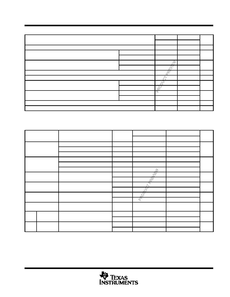
absolute maximum ratings over operating free-air temperature range (unless otherwise noted)
Supply voltage range, V
CC
¡ 0.5 V to 7 V
. . . . . . . . . . . . . . . . . . . . . . . . . . . . . . . . . . . . . . . . . . . . . . . . . . . . . . . . . .
Input voltage range, V
I
: Except I/O ports (see Note 1)
¡ 0.5 V to V
CC
+ 0.5 V
. . . . . . . . . . . . . . . . . . . . . . . . . . .
I/O ports (see Notes 1 and 2)
¡ 0.5 V to V
CC
+ 0.5 V
. . . . . . . . . . . . . . . . . . . . . . . . . . .
Output voltage range, V
O
(see Notes 1 and 2)
¡ 0.5 V to V
CC
+ 0.5 V
. . . . . . . . . . . . . . . . . . . . . . . . . . . . . . . . .
Input clamp current, I
IK
(V
I
< 0 or V
I
> V
CC
)
▒
20 mA
. . . . . . . . . . . . . . . . . . . . . . . . . . . . . . . . . . . . . . . . . . . . . . .
Output clamp current, I
OK
(V
O
< 0 or V
O
> V
CC
)
▒
50 mA
. . . . . . . . . . . . . . . . . . . . . . . . . . . . . . . . . . . . . . . . . . .
Continuous output current, I
O
(V
O
= 0 to V
CC
)
▒
35 mA
. . . . . . . . . . . . . . . . . . . . . . . . . . . . . . . . . . . . . . . . . . . . .
Continuous current through V
CC
or GND
▒
70 mA
. . . . . . . . . . . . . . . . . . . . . . . . . . . . . . . . . . . . . . . . . . . . . . . . . .
Maximum power dissipation at T
A
= 55
░
C (in still air) (see Note 3): DB package
0.6 W
. . . . . . . . . . . . . . . . . .
DW package
1.6 W
. . . . . . . . . . . . . . . . .
PW package
0.7 W
. . . . . . . . . . . . . . . . . .
Storage temperature range, T
stg
¡ 65
░
C to 150
░
C
. . . . . . . . . . . . . . . . . . . . . . . . . . . . . . . . . . . . . . . . . . . . . . . . . .
Stresses beyond those listed under "absolute maximum ratings" may cause permanent damage to the device. These are stress ratings only, and
functional operation of the device at these or any other conditions beyond those indicated under "recommended operating conditions" is not
implied. Exposure to absolute-maximum-rated conditions for extended periods may affect device reliability.
NOTES:
1. The input and output voltage ratings may be exceeded if the input and output current ratings are observed.
2. This value is limited to 7 V maximum.
3. The maximum package power dissipation is calculated using a junction temperature of 150
░
C and a board trace length of 750 mils.
SN54LV245, SN74LV245
OCTAL BUS TRANSCEIVERS
WITH 3-STATE OUTPUTS
SCLS075E ¡ JANUARY 1991 ¡ REVISED APRIL 1996
3
POST OFFICE BOX 655303
À
DALLAS, TEXAS 75265
recommended operating conditions (see Note 4)
SN54LV245
SN74LV245
UNIT
MIN
MAX
MIN
MAX
UNIT
VCC
Supply voltage
2.7
5.5
2.7
5.5
V
VIH
High level input voltage
VCC = 2.7 V to 3.6 V
2
2
V
VIH
High-level input voltage
VCC = 4.5 V to 5.5 V
3.15
3.15
V
VIL
Low level input voltage
VCC = 2.7 V to 3.6 V
0.8
0.8
V
VIL
Low-level input voltage
VCC = 4.5 V to 5.5 V
1.65
1.65
V
VI
Input voltage
0
VCC
0
VCC
V
VO
Output voltage
0
VCC
0
VCC
V
IOH
High level output current
VCC = 2.7 V to 3.6 V
¡8
¡8
mA
IOH
High-level output current
VCC = 4.5 V to 5.5 V
¡16
¡16
mA
IOL
Low level output current
VCC = 2.7 V to 3.6 V
8
8
mA
IOL
Low-level output current
VCC = 4.5 V to 5.5 V
16
16
mA
t/
v
Input transition rise or fall rate
0
50
0
50
ns / V
TA
Operating free-air temperature
¡55
125
¡40
85
░
C
NOTE 4: Unused inputs must be held high or low to prevent them from floating.
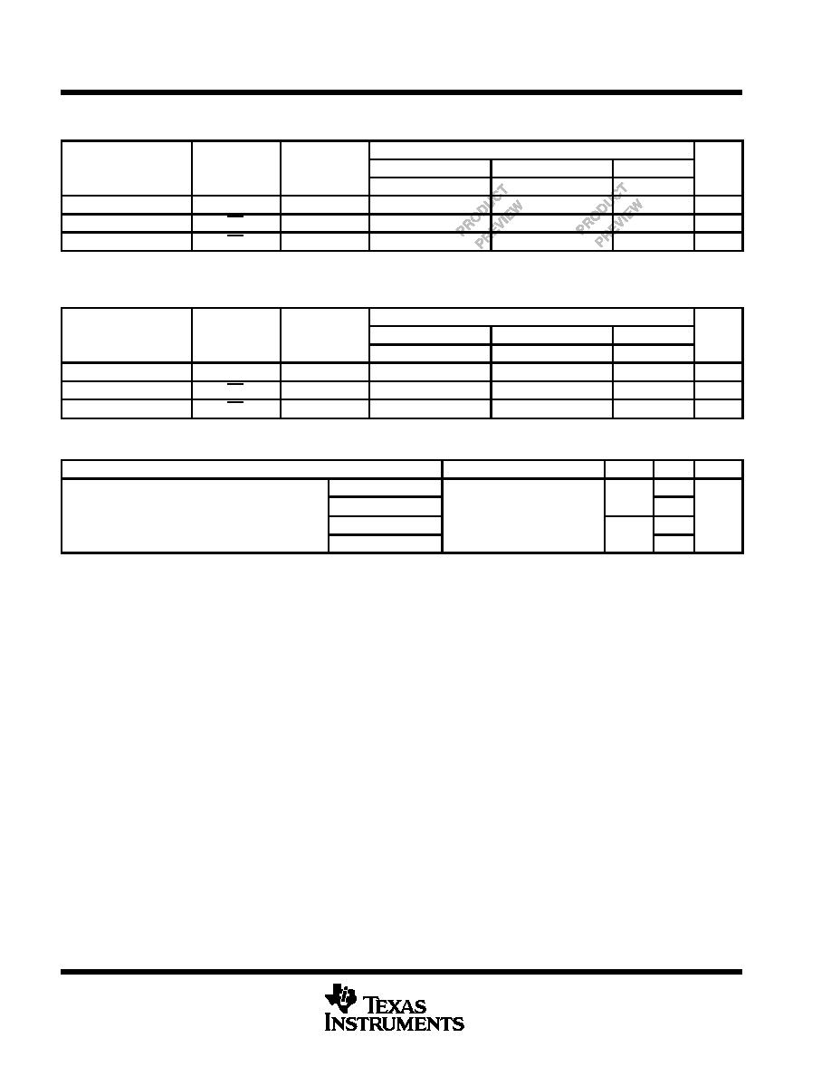
electrical characteristics over recommended operating free-air temperature range (unless
otherwise noted)
PARAMETER
TEST CONDITIONS
VCC
SN54LV245
SN74LV245
UNIT
PARAMETER
TEST CONDITIONS
VCC
MIN
TYP
MAX
MIN
TYP
MAX
UNIT
IOH = ¡100
Á
A
MIN to MAX
VCC¡0.2
VCC¡0.2
VOH
IOH = ¡8 mA
3 V
2.4
2.4
V
IOH = ¡16 mA
4.5 V
3.6
3.6
IOL = 100
Á
A
MIN to MAX
0.2
0.2
VOL
IOL = 8 mA
3 V
0.4
0.4
V
IOL = 16 mA
4.5 V
0.55
0.55
II
VI = VCC or GND
3.6 V
▒
1
▒
1
Á
A
II
VI = VCC or GND
5.5 V
▒
1
▒
1
Á
A
I
VO = VCC or GND
3.6 V
▒
5
▒
5
Á
A
IOZ
VO = VCC or GND
5.5 V
▒
5
▒
5
Á
A
ICC
VI = VCC or GND
IO = 0
3.6 V
20
20
Á
A
ICC
VI = VCC or GND,
IO = 0
5.5 V
20
20
Á
A
n
ICC
One input at VCC ¡ 0.6 V,
Other inputs at VCC or GND
3 V to 3.6 V
500
500
Á
A
Ci
Control inputs
VI = VCC or GND
3.3 V
2.5
2.5
pF
Ci
Control inputs
VI = VCC or GND
5 V
3
3
pF
C
A or B port
VO = VCC or GND
3.3 V
7
7
pF
Co
A or B port
VO = VCC or GND
5 V
8
8
pF
For conditions shown as MIN or MAX, use the appropriate values under recommended operating conditions.
For I/O ports, the parameter IOZ includes the input leakage current.
PRODUCT PREVIEW information concerns products in the formative or
design phase of development. Characteristic data and other
specifications are design goals. Texas Instruments reserves the right to
change or discontinue these products without notice.
SN54LV245, SN74LV245
OCTAL BUS TRANSCEIVERS
WITH 3-STATE OUTPUTS
SCLS075E ¡ JANUARY 1991 ¡ REVISED APRIL 1996
4
POST OFFICE BOX 655303
À
DALLAS, TEXAS 75265
switching characteristics over recommended operating free-air temperature range, C
L
= 50 pF
(unless otherwise noted) (see Figure 1)
FROM
TO
SN54LV245
PARAMETER
FROM
(INPUT)
TO
(OUTPUT)
VCC = 5 V
▒
0.5 V
VCC = 3.3 V
▒
0.3 V
VCC = 2.7 V
UNIT
(INPUT)
(OUTPUT)
MIN
TYP
MAX
MIN
TYP
MAX
MIN
MAX
tpd
A or B
B or A
8
11
8
14
18
ns
ten
OE
A or B
6
14
12
21
25
ns
tdis
OE
A or B
8
16
12
20
24
ns
switching characteristics over recommended operating free-air temperature range, C
L
= 50 pF
(unless otherwise noted) (see Figure 1)
FROM
TO
SN74LV245
PARAMETER
FROM
(INPUT)
TO
(OUTPUT)
VCC = 5 V
▒
0.5 V
VCC = 3.3 V
▒
0.3 V
VCC = 2.7 V
UNIT
(INPUT)
(OUTPUT)
MIN
TYP
MAX
MIN
TYP
MAX
MIN
MAX
tpd
A or B
B or A
8
11
8
14
18
ns
ten
OE
A or B
6
14
12
21
25
ns
tdis
OE
A or B
8
16
12
20
24
ns
operating characteristics, T
A
= 25
░
C
PARAMETER
TEST CONDITIONS
VCC
TYP
UNIT
Outputs enabled
3 3 V
36
Cpd
Power dissipation capacitance per
Outputs disabled
CL = 50 pF
f = 10 MHz
3.3 V
4
pF
Cpd
transceiver
Outputs enabled
CL = 50 F,
f = 10 MHz
5 V
46
F
Outputs disabled
5 V
4
PRODUCT PREVIEW information concerns products in the formative or
design phase of development. Characteristic data and other
specifications are design goals. Texas Instruments reserves the right to
change or discontinue these products without notice.
SN54LV245, SN74LV245
OCTAL BUS TRANSCEIVERS
WITH 3-STATE OUTPUTS
SCLS075E ¡ JANUARY 1991 ¡ REVISED APRIL 1996
5
POST OFFICE BOX 655303
À
DALLAS, TEXAS 75265
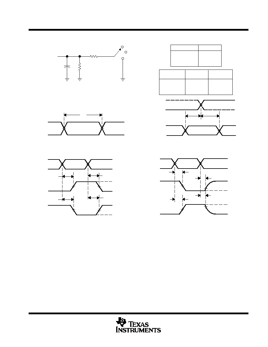
PARAMETER MEASUREMENT INFORMATION
Vm
th
tsu
From Output
Under Test
CL = 50 pF
(see Note A)
LOAD CIRCUIT
S1
Vz
Open
GND
1 k
1 k
Data Input
Timing Input
Vm
Vi
0 V
Vm
Vm
Vi
0 V
Vi
0 V
Vm
Vm
tw
Input
VOLTAGE WAVEFORMS
SETUP AND HOLD TIMES
VOLTAGE WAVEFORMS
PROPAGATION DELAY TIMES
INVERTING AND NONINVERTING OUTPUTS
VOLTAGE WAVEFORMS
PULSE DURATION
tPLH
tPHL
tPHL
tPLH
VOH
VOH
VOL
VOL
Vm
Vm
Vi
0 V
Vm
Vm
Input
Vm
Output
Control
Output
Waveform 1
S1 at Vz
(see Note B)
Output
Waveform 2
S1 at GND
(see Note B)
VOL
VOH
tPZL
tPZH
tPLZ
tPHZ
Vm
Vm
0.5
Î
Vz
0 V
Vm
VOL + 0.3 V
Vm
VOH ¡ 0.3 V
[
0 V
Vi
VOLTAGE WAVEFORMS
ENABLE AND DISABLE TIMES
LOW- AND HIGH-LEVEL ENABLING
Output
Output
tPLH/tPHL
tPLZ/tPZL
tPHZ/tPZH
Open
Vz
GND
TEST
S1
0.5
Î
VCC
VCC
2
Î
VCC
1.5 V
2.7 V
6 V
WAVEFORM
CONDITION
VCC = 4.5 V
to 5.5 V
VCC = 2.7 V
to 3.6 V
Vm
Vi
Vz
NOTES: A. CL includes probe and jig capacitance.
B. Waveform 1 is for an output with internal conditions such that the output is low except when disabled by the output control.
Waveform 2 is for an output with internal conditions such that the output is high except when disabled by the output control.
C. All input pulses are supplied by generators having the following characteristics: PRR
10 MHz, ZO = 50
, tr
2.5 ns, tf
2.5 ns.
D. The outputs are measured one at a time with one transition per measurement.
E. tPLZ and tPHZ are the same as tdis.
F. tPZL and tPZH are the same as ten.
G. tPLH and tPHL are the same as tpd.
Figure 1. Load Circuit and Voltage Waveforms