
SN54LV244A, SN74LV244A
OCTAL BUFFERS/DRIVERS
WITH 3-STATE OUTPUTS
SCLS383B SEPTEMBER 1997 REVISED JUNE 1998
1
POST OFFICE BOX 655303
·
DALLAS, TEXAS 75265
D
EPIC
TM
(Enhanced-Performance Implanted
CMOS) Process
D
Typical V
OLP
(Output Ground Bounce)
< 0.8 V at V
CC
, T
A
= 25
°
C
D
Typical V
OHV
(Output V
OH
Undershoot)
> 2 V at V
CC
, T
A
= 25
°
C
D
Latch-Up Performance Exceeds 250 mA Per
JESD 17
D
ESD Protection Exceeds 2000 V Per
MIL-STD-883, Method 3015; Exceeds 200 V
Using Machine Model (C = 200 pF, R = 0)
D
Package Options Include Plastic
Small-Outline (DW, NS), Shrink
Small-Outline (DB), Thin Very Small-Outline
(DGV), and Thin Shrink Small-Outline (PW)
Packages, Ceramic Flat (W) Packages, Chip
Carriers (FK), and DIPs (J)
description
These octal buffers/line drivers are designed for
2-V to 5.5-V V
CC
operation.
The 'LV244A devices are designed specifically to
improve both the performance and density of
3-state memory address drivers, clock drivers,
and bus-oriented receivers and transmitters.
These devices are organized as two 4-bit line
drivers with separate output-enable (OE) inputs.
When OE is low, the device passes data from the
A inputs to the Y outputs. When OE is high, the
outputs are in the high-impedance state.
To ensure the high-impedance state during power up or power down, OE should be tied to V
CC
through a pullup
resistor; the minimum value of the resistor is determined by the current-sinking capability of the driver.
The SN54LV244A is characterized for operation over the full military temperature range of 55
°
C to 125
°
C.
The SN74LV244A is characterized for operation from 40
°
C to 85
°
C.
FUNCTION TABLE
(each buffer)
INPUTS
OUTPUT
OE
A
Y
L
H
H
L
L
L
H
X
Z
Copyright
©
1998, Texas Instruments Incorporated
UNLESS OTHERWISE NOTED this document contains PRODUCTION
DATA information current as of publication date. Products conform to
specifications per the terms of Texas Instruments standard warranty.
Production processing does not necessarily include testing of all
parameters.
EPIC is a trademark of Texas Instruments Incorporated.
Please be aware that an important notice concerning availability, standard warranty, and use in critical applications of
Texas Instruments semiconductor products and disclaimers thereto appears at the end of this data sheet.
1
2
3
4
5
6
7
8
9
10
20
19
18
17
16
15
14
13
12
11
1OE
1A1
2Y4
1A2
2Y3
1A3
2Y2
1A4
2Y1
GND
V
CC
2OE
1Y1
2A4
1Y2
2A3
1Y3
2A2
1Y4
2A1
SN54LV244A . . . J OR W PACKAGE
SN74LV244A . . . DB, DGV, DW, NS, OR PW PACKAGE
(TOP VIEW)
3
2 1 20 19
9 10 11 12 13
4
5
6
7
8
18
17
16
15
14
1Y1
2A4
1Y2
2A3
1Y3
1A2
2Y3
1A3
2Y2
1A4
SN54LV244A . . . FK PACKAGE
(TOP VIEW)
2Y4
1A1
1OE
1Y4
2A2
2OE
2Y1
GND
2A1
V
CC
SN54LV244A, SN74LV244A
OCTAL BUFFERS/DRIVERS
WITH 3-STATE OUTPUTS
SCLS383B SEPTEMBER 1997 REVISED JUNE 1998
2
POST OFFICE BOX 655303
·
DALLAS, TEXAS 75265
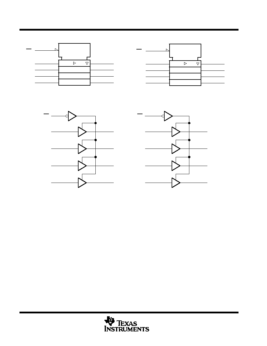
logic symbol
2
1A1
4
1A2
6
1A3
8
1A4
EN
1
1Y1
18
1Y2
16
1Y3
14
1Y4
12
11
2A1
13
2A2
15
2A3
17
2A4
EN
19
2Y1
9
2Y2
7
2Y3
5
2Y4
3
1OE
2OE
This symbol is in accordance with ANSI/IEEE Std 91-1984 and IEC Publication 617-12.
logic diagram (positive logic)
1
2
18
1Y1
1OE
1A1
4
16
1Y2
1A2
6
14
1Y3
1A3
8
12
1Y4
1A4
19
11
9
2Y1
2OE
2A1
13
7
2Y2
2A2
15
5
2Y3
2A3
17
3
2Y4
2A4
absolute maximum ratings over operating free-air temperature range (unless otherwise noted)
Supply voltage range, V
CC
0.5 V to 7 V
. . . . . . . . . . . . . . . . . . . . . . . . . . . . . . . . . . . . . . . . . . . . . . . . . . . . . . . . . .
Input voltage range, V
I
(see Note 1)
0.5 V to 7 V
. . . . . . . . . . . . . . . . . . . . . . . . . . . . . . . . . . . . . . . . . . . . . . . . . .
Output voltage range applied in the high or low state, V
O
(see Notes 1 and 2)
0.5 V to V
CC
+ 0.5 V
. . . . . .
Output voltage range applied in high-impedance or power-off state, V
O
(see Note 1)
0.5 V to 7 V
. . . . . . .
Input clamp current, I
IK
(V
I
< 0)
20 mA
. . . . . . . . . . . . . . . . . . . . . . . . . . . . . . . . . . . . . . . . . . . . . . . . . . . . . . . . . . .
Output clamp current, I
OK
(V
O
< 0 or V
O
> V
CC
)
±
50 mA
. . . . . . . . . . . . . . . . . . . . . . . . . . . . . . . . . . . . . . . . . . . .
Continuous output current, I
O
(V
O
= 0 to V
CC
)
±
35 mA
. . . . . . . . . . . . . . . . . . . . . . . . . . . . . . . . . . . . . . . . . . . . . .
Continuous current through V
CC
or GND
±
70 mA
. . . . . . . . . . . . . . . . . . . . . . . . . . . . . . . . . . . . . . . . . . . . . . . . . . .
Package thermal impedance,
JA
(see Note 3): DB package
115
°
C/W
. . . . . . . . . . . . . . . . . . . . . . . . . . . . . . . . .
DGV package
146
°
C/W
. . . . . . . . . . . . . . . . . . . . . . . . . . . . . . .
DW package
97
°
C/W
. . . . . . . . . . . . . . . . . . . . . . . . . . . . . . . . .
NS package
100
°
C/W
. . . . . . . . . . . . . . . . . . . . . . . . . . . . . . . . .
PW package
128
°
C/W
. . . . . . . . . . . . . . . . . . . . . . . . . . . . . . . .
Storage temperature range, T
stg
65
°
C to 150
°
C
. . . . . . . . . . . . . . . . . . . . . . . . . . . . . . . . . . . . . . . . . . . . . . . . . . .
Stresses beyond those listed under "absolute maximum ratings" may cause permanent damage to the device. These are stress ratings only, and
functional operation of the device at these or any other conditions beyond those indicated under "recommended operating conditions" is not
implied. Exposure to absolute-maximum-rated conditions for extended periods may affect device reliability.
NOTES:
1. The input and output voltage ratings may be exceeded if the input and output current ratings are observed.
2. This value is limited to 7 V maximum.
3. The package thermal impedance is calculated in accordance with JESD 51.
SN54LV244A, SN74LV244A
OCTAL BUFFERS/DRIVERS
WITH 3-STATE OUTPUTS
SCLS383B SEPTEMBER 1997 REVISED JUNE 1998
3
POST OFFICE BOX 655303
·
DALLAS, TEXAS 75265
recommended operating conditions (see Note 4)
SN54LV244A
SN74LV244A
UNIT
MIN
MAX
MIN
MAX
UNIT
VCC
Supply voltage
2
5.5
2
5.5
V
VCC = 2 V
1.5
1.5
VIH
High level input voltage
VCC = 2.3 V to 2.7 V
VCC
×
0.7
VCC
×
0.7
V
VIH
High-level input voltage
VCC = 3 V to 3.6 V
VCC
×
0.7
VCC
×
0.7
V
VCC = 4.5 V to 5.5 V
VCC
×
0.7
VCC
×
0.7
VCC = 2 V
0.5
0.5
VIL
Low level input voltage
VCC = 2.3 V to 2.7 V
VCC
×
0.3
VCC
×
0.3
V
VIL
Low-level input voltage
VCC = 3 V to 3.6 V
VCC
×
0.3
VCC
×
0.3
V
VCC = 4.5 V to 5.5 V
VCC
×
0.3
VCC
×
0.3
VI
Input voltage
0
5.5
0
5.5
V
VO
Output voltage
High or low state
0
VCC
0
VCC
V
VO
Output voltage
3-state
0
5.5
0
5.5
V
VCC = 2 V
50
50
µ
A
IOH
High level output current
VCC = 2.3 V to 2.7 V
2
2
IOH
High-level output current
VCC = 3 V to 3.6 V
8
8
mA
VCC = 4.5 V to 5.5 V
16
16
VCC = 2 V
50
50
µ
A
IOL
Low level output current
VCC = 2.3 V to 2.7 V
2
2
IOL
Low-level output current
VCC = 3 V to 3.6 V
8
8
mA
VCC = 4.5 V to 5.5 V
16
16
VCC = 2.3 V to 2.7 V
0
200
0
200
t/
v
Input transition rise or fall rate
VCC = 3 V to 3.6 V
0
100
0
100
ns/V
VCC = 4.5 V to 5.5 V
0
20
0
20
TA
Operating free-air temperature
55
125
40
85
°
C
NOTE 4: All unused inputs of the device must be held at VCC or GND to ensure proper device operation. Refer to the TI application report,
Implications of Slow or Floating CMOS Inputs, literature number SCBA004.
PRODUCT PREVIEW information concerns products in the formative or
design phase of development. Characteristic data and other
specifications are design goals. Texas Instruments reserves the right to
change or discontinue these products without notice.
SN54LV244A, SN74LV244A
OCTAL BUFFERS/DRIVERS
WITH 3-STATE OUTPUTS
SCLS383B SEPTEMBER 1997 REVISED JUNE 1998
4
POST OFFICE BOX 655303
·
DALLAS, TEXAS 75265
electrical characteristics over recommended operating free-air temperature range (unless
otherwise noted)
PARAMETER
TEST CONDITIONS
V
SN54LV244A
SN74LV244A
UNIT
PARAMETER
TEST CONDITIONS
VCC
MIN
TYP
MAX
MIN
TYP
MAX
UNIT
IOH = 50
µ
A
2 V to 5.5 V
VCC0.1
VCC0.1
VOH
IOH = 2 mA
2.3 V
2
2
V
VOH
IOH = 8 mA
3 V
2.48
2.48
V
IOH = 16 mA
4.5 V
3.8
3.8
IOL = 50
µ
A
2 V to 5.5 V
0.1
0.1
VOL
IOL = 2 mA
2.3 V
0.4
0.4
V
VOL
IOL = 8 mA
3 V
0.44
0.44
V
IOL = 16 mA
4.5 V
0.55
0.55
II
VI = VCC or GND
5.5 V
±
1
±
1
µ
A
IOZ
VO = VCC or GND
5.5 V
±
5
±
5
µ
A
ICC
VI = VCC or GND,
IO = 0
5.5 V
20
20
µ
A
Ioff
VI or VO = 0 to 5.5 V
0 V
20
20
µ
A
Ci
VI = VCC or GND
3.3 V
2.3
2.3
pF
Ci
VI = VCC or GND
5 V
2.3
2.3
pF
switching characteristics over recommended operating free-air temperature range,
V
CC
= 2.5 V
±
0.2 V (unless otherwise noted) (see Figure 1)
PARAMETER
FROM
TO
LOAD
TA = 25
°
C
SN54LV244A
SN74LV244A
UNIT
PARAMETER
(INPUT)
(OUTPUT)
CAPACITANCE
MIN
TYP
MAX
MIN
MAX
MIN
MAX
UNIT
tpd*
A
Y
7.5
12.5
1
15
1
15
ten*
OE
Y
CL = 15 pF
8.9
14.6
1
17
1
17
ns
tdis*
OE
Y
9.1
14.1
1
16
1
16
tpd
A
Y
9.5
15.3
1
18
1
18
ten
OE
Y
CL = 50 pF
10.8
17.8
1
21
1
21
ns
tdis
OE
Y
CL = 50 pF
13.4
19.2
1
21
1
21
ns
tsk(o)
2
2
* On products compliant to MIL-PRF-38535, this parameter is not production tested.
Skew between any two outputs of the same package switching in the same direction
switching characteristics over recommended operating free-air temperature range,
V
CC
= 3.3 V
±
0.3 V (unless otherwise noted) (see Figure 1)
PARAMETER
FROM
TO
LOAD
TA = 25
°
C
SN54LV244A
SN74LV244A
UNIT
PARAMETER
(INPUT)
(OUTPUT)
CAPACITANCE
MIN
TYP
MAX
MIN
MAX
MIN
MAX
UNIT
tpd*
A
Y
5.4
8.4
1
10
1
10
ten*
OE
Y
CL = 15 pF
6.3
10.6
1
12.5
1
12.5
ns
tdis*
OE
Y
7.6
11
1
13
1
13
tpd
A
Y
6.8
11.9
1
13.5
1
13.5
ten
OE
Y
CL = 50 pF
7.8
14.1
1
16
1
16
ns
tdis
OE
Y
CL = 50 pF
11
16
1
18
1
18
ns
tsk(o)
1.5
1.5
* On products compliant to MIL-PRF-38535, this parameter is not production tested.
Skew between any two outputs of the same package switching in the same direction
PRODUCT PREVIEW information concerns products in the formative or
design phase of development. Characteristic data and other
specifications are design goals. Texas Instruments reserves the right to
change or discontinue these products without notice.
SN54LV244A, SN74LV244A
OCTAL BUFFERS/DRIVERS
WITH 3-STATE OUTPUTS
SCLS383B SEPTEMBER 1997 REVISED JUNE 1998
5
POST OFFICE BOX 655303
·
DALLAS, TEXAS 75265
switching characteristics over recommended operating free-air temperature range,
V
CC
= 5 V
±
0.5 V (unless otherwise noted) (see Figure 1)
PARAMETER
FROM
TO
LOAD
TA = 25
°
C
SN54LV244A
SN74LV244A
UNIT
PARAMETER
(INPUT)
(OUTPUT)
CAPACITANCE
MIN
TYP
MAX
MIN
MAX
MIN
MAX
UNIT
tpd*
A
Y
3.9
5.5
1
6.5
1
6.5
ten*
OE
Y
CL = 15 pF
4.5
7.3
1
8.5
1
8.5
ns
tdis*
OE
Y
6.5
12.2
1
13.5
1
13.5
tpd
A
Y
4.9
7.5
1
8.5
1
8.5
ten
OE
Y
CL = 50 pF
5.6
9.3
1
10.5
1
10.5
ns
tdis
OE
Y
CL = 50 pF
8.8
14.2
1
15.5
1
15.5
ns
tsk(o)
1
1
* On products compliant to MIL-PRF-38535, this parameter is not production tested.
Skew between any two outputs of the same package switching in the same direction
noise characteristics, V
CC
= 3.3 V, C
L
= 50 pF, T
A
= 25
°
C (see Note 5
)
PARAMETER
SN74LV244A
UNIT
PARAMETER
MIN
TYP
MAX
UNIT
VOL(P)
Quiet output, maximum dynamic VOL
0.55
V
VOL(V)
Quiet output, minimum dynamic VOL
0.5
V
VOH(V)
Quiet output, minimum dynamic VOH
2.9
V
VIH(D)
High-level dynamic input voltage
2.31
V
VIL(D)
Low-level dynamic input voltage
0.99
V
NOTE 5: Characteristics are for surface-mount packages only.
operating characteristics, T
A
= 25
°
C
PARAMETER
TEST CONDITIONS
VCC
TYP
UNIT
Cpd
Power dissipation capacitance
CL = 50 pF
f = 10 MHz
3.3 V
14
pF
Cpd
Power dissi ation ca acitance
CL = 50 F,
f = 10 MHz
5 V
16
F
PRODUCT PREVIEW information concerns products in the formative or
design phase of development. Characteristic data and other
specifications are design goals. Texas Instruments reserves the right to
change or discontinue these products without notice.