SN54HC645, SN74HC645
OCTAL BUS TRANSCEIVERS
WITH 3-STATE OUTPUTS
SCLS304A JANUARY 1996 REVISED MAY 1997
1
POST OFFICE BOX 655303
·
DALLAS, TEXAS 75265
D
True Logic
D
High-Current 3-State Outputs Can Drive up
to 15 LSTTL Loads
D
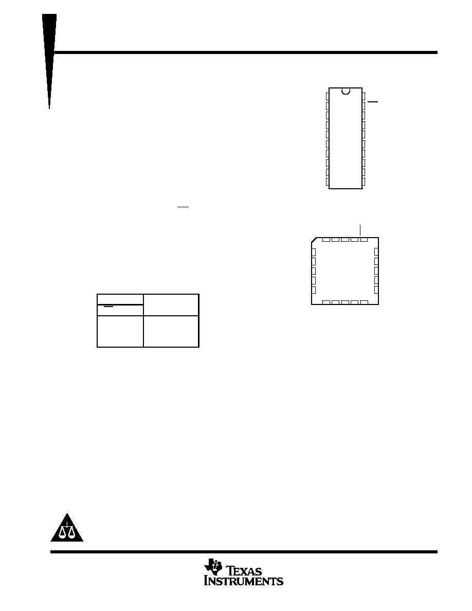
Package Options Include Plastic
Small-Outline (DW) and Ceramic Flat (W)
Packages, Ceramic Chip Carriers (FK), and
Standard Plastic (N) and Ceramic (J)
300-mil DIPs
description
These octal bus transceivers are designed for
asynchronous two-way communication between
data buses. These devices transmit data from the
A bus to the B bus or from the B bus to the A bus,
depending upon the level at the direction-control
(DIR) input. The output-enable (OE) input can be
used to disable the device so the buses are
effectively isolated.
The SN54HC645 is characterized for operation
over the full military temperature range of 55
°
C
to 125
°
C. The SN74HC645 is characterized for
operation from 40
°
C to 85
°
C.
FUNCTION TABLE
INPUTS
OPERATION
OE
DIR
OPERATION
L
L
B data to A bus
L
H
A data to B bus
H
X
Isolation
Copyright
©
1997, Texas Instruments Incorporated
PRODUCTION DATA information is current as of publication date.
Products conform to specifications per the terms of Texas Instruments
standard warranty. Production processing does not necessarily include
testing of all parameters.
Please be aware that an important notice concerning availability, standard warranty, and use in critical applications of
Texas Instruments semiconductor products and disclaimers thereto appears at the end of this data sheet.
SN54HC645 . . . J OR W PACKAGE
SN74HC645 . . . DW OR N PACKAGE
(TOP VIEW)
SN54HC645 . . . FK PACKAGE
(TOP VIEW)
1
2
3
4
5
6
7
8
9
10
20
19
18
17
16
15
14
13
12
11
DIR
A1
A2
A3
A4
A5
A6
A7
A8
GND
V
CC
OE
B1
B2
B3
B4
B5
B6
B7
B8
3
2
1 20 19
9 10 11 12 13
4
5
6
7
8
18
17
16
15
14
B1
B2
B3
B4
B5
A3
A4
A5
A6
A7
A2
A1
DIR
B7
B6
OE
A8
GND
B8
V
CC

SN54HC645, SN74HC645
OCTAL BUS TRANSCEIVERS
WITH 3-STATE OUTPUTS
SCLS304A JANUARY 1996 REVISED MAY 1997
2
POST OFFICE BOX 655303
·
DALLAS, TEXAS 75265
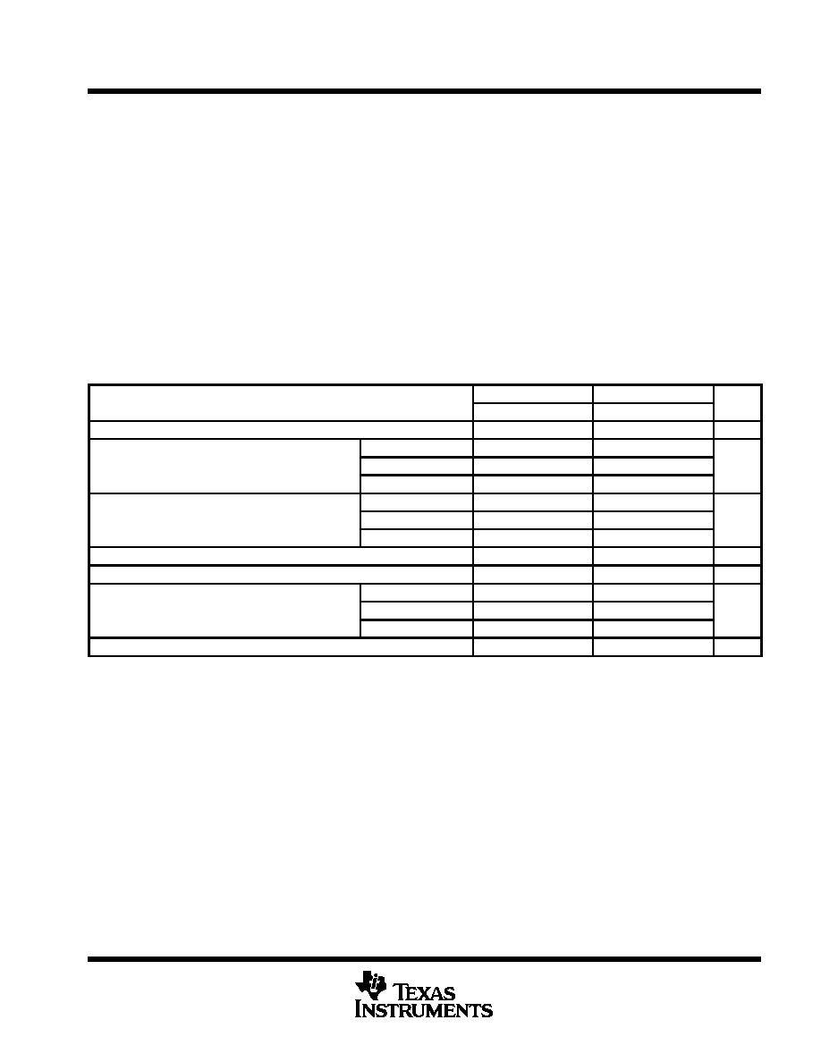
logic symbol
B2
17
B3
16
B4
15
A5
6
A6
7
A7
8
A8
9
A2
3
A3
4
A4
5
OE
A1
2
G3
19
3 EN2 [AB]
B5
14
B6
13
B7
12
B8
11
B1
18
3 EN1 [BA]
1
DIR
1
2
This symbol is in accordance with ANSI/IEEE Std 91-1984 and IEC Publication 617-12.
logic diagram (positive logic)
A1
B1
OE
DIR
To Seven Other Transceivers
19
1
2
18
SN54HC645, SN74HC645
OCTAL BUS TRANSCEIVERS
WITH 3-STATE OUTPUTS
SCLS304A JANUARY 1996 REVISED MAY 1997
3
POST OFFICE BOX 655303
·
DALLAS, TEXAS 75265
absolute maximum ratings over operating free-air temperature range
Supply voltage range, V
CC
0.5 V to 7 V
. . . . . . . . . . . . . . . . . . . . . . . . . . . . . . . . . . . . . . . . . . . . . . . . . . . . . . . . . .
Input clamp current, I
IK
(V
I
< 0 or V
I
> V
CC
) (see Note 1)
±
20 mA
. . . . . . . . . . . . . . . . . . . . . . . . . . . . . . . . . . . .
Output clamp current, I
OK
(V
O
< 0 or V
O
> V
CC
) (see Note 1)
±
20 mA
. . . . . . . . . . . . . . . . . . . . . . . . . . . . . . . .
Continuous output current, I
O
(V
O
= 0 to V
CC
)
±
35 mA
. . . . . . . . . . . . . . . . . . . . . . . . . . . . . . . . . . . . . . . . . . . . . .
Continuous current through V
CC
or GND
±
70 mA
. . . . . . . . . . . . . . . . . . . . . . . . . . . . . . . . . . . . . . . . . . . . . . . . . . .
Package thermal impedance,
JA
(see Note 2): DW package
97
°
C/W
. . . . . . . . . . . . . . . . . . . . . . . . . . . . . . . . .
N package
67
°
C/W
. . . . . . . . . . . . . . . . . . . . . . . . . . . . . . . . . . .
Storage temperature range, T
stg
65
°
C to 150
°
C
. . . . . . . . . . . . . . . . . . . . . . . . . . . . . . . . . . . . . . . . . . . . . . . . . . .
Stresses beyond those listed under "absolute maximum ratings" may cause permanent damage to the device. These are stress ratings only, and
functional operation of the device at these or any other conditions beyond those indicated under "recommended operating conditions" is not
implied. Exposure to absolute-maximum-rated conditions for extended periods may affect device reliability.
NOTES:
1. The input and output voltage ratings may be exceeded if the input and output current ratings are observed.
2. The package thermal impedance is calculated in accordance with JESD 51, except for through-hole packages, which use a trace
length of zero.
recommended operating conditions
SN54HC645
SN74HC645
UNIT
MIN
NOM
MAX
MIN
NOM
MAX
UNIT
VCC
Supply voltage
2
5
6
2
5
6
V
VCC = 2 V
1.5
1.5
VIH
High-level input voltage
VCC = 4.5 V
3.15
3.15
V
VCC = 6 V
4.2
4.2
VCC = 2 V
0
0.5
0
0.5
VIL
Low-level input voltage
VCC = 4.5 V
0
1.35
0
1.35
V
VCC = 6 V
0
1.8
0
1.8
VI
Input voltage
0
VCC
0
VCC
V
VO
Output voltage
0
VCC
0
VCC
V
VCC = 2 V
0
1000
0
1000
tt
Input transition (rise and fall) time
VCC = 4.5 V
0
500
0
500
ns
VCC = 6 V
0
400
0
400
TA
Operating free-air temperature
55
125
40
85
°
C
SN54HC645, SN74HC645
OCTAL BUS TRANSCEIVERS
WITH 3-STATE OUTPUTS
SCLS304A JANUARY 1996 REVISED MAY 1997
4
POST OFFICE BOX 655303
·
DALLAS, TEXAS 75265
electrical characteristics over recommended operating free-air temperature range (unless
otherwise noted)
PARAMETER
TEST CONDITIONS
VCC
TA = 25
°
C
SN54HC645
SN74HC645
UNIT
PARAMETER
TEST CONDITIONS
VCC
MIN
TYP
MAX
MIN
MAX
MIN
MAX
UNIT
2 V
1.9
1.998
1.9
1.9
IOH = 20
µ
A
4.5 V
4.4
4.499
4.4
4.4
VOH
VI = VIH or VIL
6 V
5.9
5.999
5.9
5.9
V
IOH = 6 mA
4.5 V
3.98
4.3
3.7
3.84
IOH = 7.8 mA
6 V
5.48
5.8
5.2
5.34
2 V
0.002
0.1
0.1
0.1
IOL = 20
µ
A
4.5 V
0.001
0.1
0.1
0.1
VOL
VI = VIH or VIL
6 V
0.001
0.1
0.1
0.1
V
IOL = 6 mA
4.5 V
0.17
0.26
0.4
0.33
IOL = 7.8 mA
6 V
0.15
0.26
0.4
0.33
II
DIR or OE
VI = VCC or 0
6 V
±
0.1
±
100
±
1000
±
1000
nA
IOZ
A or B
VO = VCC or 0
6 V
±
0.01
±
0.5
±
10
±
5
µ
A
ICC
VI = VCC or 0,
IO = 0
6 V
8
160
80
µ
A
Ci
DIR or OE
2 V to 6 V
3
10
10
10
pF
switching characteristics over recommended operating free-air temperature range, C
L
= 50 pF
(unless otherwise noted) (see Figure 1)
PARAMETER
FROM
TO
VCC
TA = 25
°
C
SN54HC645
SN74HC645
UNIT
PARAMETER
(INPUT)
(OUTPUT)
VCC
MIN
TYP
MAX
MIN
MAX
MIN
MAX
UNIT
2 V
40
105
160
130
tpd
A or B
B or A
4.5 V
15
21
32
26
ns
6 V
12
18
27
22
2 V
125
230
340
290
ten
OE
A or B
4.5 V
23
46
68
58
ns
6 V
20
39
58
49
2 V
74
200
300
250
tdis
OE
A or B
4.5 V
25
40
60
50
ns
6 V
21
34
51
43
2 V
20
60
90
75
tt
A or B
4.5 V
8
12
18
15
ns
6 V
6
10
15
13
SN54HC645, SN74HC645
OCTAL BUS TRANSCEIVERS
WITH 3-STATE OUTPUTS
SCLS304A JANUARY 1996 REVISED MAY 1997
5
POST OFFICE BOX 655303
·
DALLAS, TEXAS 75265
switching characteristics over recommended operating free-air temperature range, C
L
= 150 pF
(unless otherwise noted) (see Figure 1)
PARAMETER
FROM
TO
VCC
TA = 25
°
C
SN54HC645
SN74HC645
UNIT
PARAMETER
(INPUT)
(OUTPUT)
VCC
MIN
TYP
MAX
MIN
MAX
MIN
MAX
UNIT
2 V
54
135
200
170
tpd
A or B
B or A
4.5 V
18
27
40
34
ns
6 V
15
23
34
29
2 V
150
270
405
335
ten
OE
A or B
4.5 V
31
54
81
67
ns
6 V
25
46
69
56
2 V
45
210
315
265
tt
A or B
4.5 V
17
42
63
53
ns
6 V
13
36
53
45
operating characteristics, T
A
= 25
°
C
PARAMETER
TEST CONDITIONS
TYP
UNIT
Cpd
Power dissipation capacitance per transceiver
No load
40
pF