SN74GTLPH16927
18-BIT LVTTL-TO-GTLP BUS TRANSCEIVER
WITH SOURCE-SYNCHRONOUS CLOCK OUTPUTS
SCES413 OCTOBER 2002
1
POST OFFICE BOX 655303
·
DALLAS, TEXAS 75265
D
Member of the Texas Instruments
Widebus
Family
D
TI-OPC
Circuitry Limits Ringing on
Unevenly Loaded Backplanes
D
OEC
Circuitry Improves Signal Integrity
and Reduces Electromagnetic Interference
D
Bidirectional Interface Between GTLP
Signal Levels and LVTTL Logic Levels
D
GTLP Buffered SYSCLK Signal (SSCLK) for
Source-Synchronous Applications
D
LVTTL Interfaces Are 5-V Tolerant
D
Medium-Drive GTLP Outputs (50 mA)
D
LVTTL Outputs (24 mA/24 mA)
D
GTLP Rise and Fall Times Designed for
Optimal Data-Transfer Rate and Signal
Integrity in Distributed Loads
D
I
off
, Power-Up 3-State, and BIAS V
CC
Support Live Insertion
D
Bus Hold on A-Port Data Inputs
D
Distributed V
CC
and GND Pins Minimize
High-Speed Switching Noise
D
Latch-Up Performance Exceeds 100 mA Per
JESD 78, Class II
D
ESD Protection Exceeds JESD 22
2000-V Human-Body Model (A114-A)
200-V Machine Model (A115-A)
1000-V Charged-Device Model (C101)
description/ordering information
The SN74GTLPH16927 is a medium-drive, 18-bit bus transceiver that provides LVTTL-to-GTLP and
GTLP-to-LVTTL signal-level translation. The device allows for transparent and latched modes of data transfer.
Additionally, with the use of the clock-mode select (CMS) input, the device can be used in source-synchronous
and clock-synchronous applications. Source-synchronous applications require the skew between the clock
output and data output to be minimized for optimum maximum-frequency system performance. In order to
reduce this skew, a flexible setup-time adjustment (FSTA) feature is incorporated into the device that sets a
predetermined delay between the clock and data. The CMS and direction (DIR) inputs control the mode of the
device.
ORDERING INFORMATION
TA
PACKAGE
ORDERABLE
PART NUMBER
TOP-SIDE
MARKING
TSSOP DGG
Tape and reel
SN74GTLPH16927GR
GTLPH16927
40
°
C to 85
°
C
TVSOP DGV
Tape and reel
SN74GTLPH16927VR
GL927
VFBGA GQL
Tape and reel
SN74GTLPH16927KR
GL927
Package drawings, standard packing quantities, thermal data, symbolization, and PCB design guidelines
are available at www.ti.com/sc/package.
Copyright
2002, Texas Instruments Incorporated
Please be aware that an important notice concerning availability, standard warranty, and use in critical applications of
Texas Instruments semiconductor products and disclaimers thereto appears at the end of this data sheet.
OEC, TI-OPC, and Widebus are trademarks of Texas Instruments.
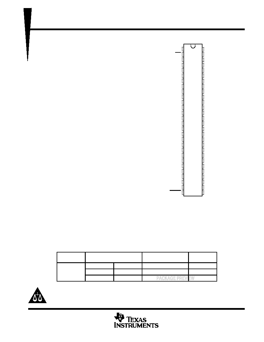
DGG OR DGV PACKAGE
(TOP VIEW)
1
2
3
4
5
6
7
8
9
10
11
12
13
14
15
16
17
18
19
20
21
22
23
24
25
26
27
28
56
55
54
53
52
51
50
49
48
47
46
45
44
43
42
41
40
39
38
37
36
35
34
33
32
31
30
29
DIR
OE
A1
GND
A2
A3
V
CC
A4
A5
A6
GND
A7
A8
A9
A10
A11
A12
GND
A13
A14
A15
V
CC
A16
A17
GND
A18
CLKOUT
CKOE
FSTA
BIAS V
CC
B1
GND
B2
B3
V
REF
B4
B5
B6
GND
B7
B8
B9
B10
B11
B12
GND
B13
B14
B15
CMS
B16
B17
GND
B18
SSCLK
SYSCLK
PRODUCTION DATA information is current as of publication date.
Products conform to specifications per the terms of Texas Instruments
standard warranty. Production processing does not necessarily include
testing of all parameters.

SN74GTLPH16927
18-BIT LVTTL-TO-GTLP BUS TRANSCEIVER
WITH SOURCE-SYNCHRONOUS CLOCK OUTPUTS
SCES413 OCTOBER 2002
2
POST OFFICE BOX 655303
·
DALLAS, TEXAS 75265
description/ordering information (continued)
The system clock (SYSCLK) and CLKOUT pins are LVTTL compatible, while the source-synchronous I/O is
GTLP compatible. The benefits include compensation for output-to-output skew coming from the driver itself,
and compensation for process skew if more than one driver is used. The device provides a high-speed interface
between cards operating at LVTTL logic levels and a backplane operating at GTLP signal levels. High-speed
(about three times faster than standard TTL or LVTTL) backplane operation is a direct result of GTLP's reduced
output swing (<1 V), reduced input threshold levels, improved differential input, OEC
circuitry, and TI-OPC
circuitry. Improved GTLP OEC and TI-OPC circuits minimize bus-settling time and have been designed and
tested using several backplane models. The medium drive allows incident-wave switching in heavily loaded
backplanes with equivalent load impedance down to 11
.
GTLP is the Texas Instruments derivative of the Gunning Transceiver Logic (GTL) JEDEC standard JESD 8-3.
The ac specification of the SN74GTLPH16927 is given only at the preferred higher noise-margin GTLP, but the
user has the flexibility of using this device at either GTL (V
TT
= 1.2 V and V
REF
= 0.8 V) or GTLP (V
TT
= 1.5 V
and V
REF
= 1 V) signal levels. For information on using GTLP devices in FB+/BTL applications, refer to TI
application reports, Texas Instruments GTLP Frequently Asked Questions,
literature number SCEA019, and
GTLP in BTL Applications, literature number SCEA017.
Normally, the B port operates at GTLP signal levels. The A-port and control inputs operate at LVTTL logic levels,
but are 5-V tolerant and are compatible with TTL and 5-V CMOS inputs. V
REF
is the B-port differential input
reference voltage.
This device is fully specified for live-insertion applications using I
off
, power-up 3-state, and BIAS V
CC
. The I
off
circuitry disables the outputs, preventing damaging current backflow through the device when it is powered
down. The power-up 3-state circuitry places the outputs in the high-impedance state during power up and power
down, which prevents driver conflict. The BIAS V
CC
circuitry precharges and preconditions the B-port
input/output connections, preventing disturbance of active data on the backplane during card insertion or
removal, and permits true live-insertion capability.
This GTLP device features TI-OPC circuitry, which actively limits the overshoot caused by improperly
terminated backplanes, unevenly distributed cards, or empty slots during low-to-high signal transitions. This
improves signal integrity, which allows adequate noise margin to be maintained at higher frequencies.
Active bus-hold circuitry holds unused or undriven LVTTL data inputs at a valid logic state. Use of pullup or
pulldown resistors with the bus-hold circuitry is not recommended.
When V
CC
is between 0 and 1.5 V, the device is in the high-impedance state during power up or power down.
However, to ensure the high-impedance state above 1.5 V, the output-enable (OE) input should be tied to V
CC
through a pullup resistor; the minimum value of the resistor is determined by the current-sinking capability of
the driver.
SN74GTLPH16927
18-BIT LVTTL-TO-GTLP BUS TRANSCEIVER
WITH SOURCE-SYNCHRONOUS CLOCK OUTPUTS
SCES413 OCTOBER 2002
3
POST OFFICE BOX 655303
·
DALLAS, TEXAS 75265
terminal assignments
1
2
3
4
5
6
A
A1
OE
DIR
FSTA
BIAS VCC
B1
B
A3
A2
GND
GND
B2
B3
C
A5
A4
VCC
VREF
B4
B5
D
A7
A6
GND
GND
B6
B7
E
A9
A8
B8
B9
F
A10
A11
B11
B10
G
A12
A13
GND
GND
B13
B12
H
A14
A15
VCC
CMS
B15
B14
J
A16
A17
GND
GND
B17
B16
K
A18
CLKOUT
CKOE
SYSCLK
SSCLK
B18
functional description
The SN74GTLPH16927 is a medium-drive (50 mA), 18-bit bus transceiver containing D-type latches and D-type
flip-flops for data-path operation in transparent or latched modes and can replace any of the functions shown
in Table 1. Data polarity is noninverting.
Table 1. SN74GTLPH16927 Bus-Transceiver Replacement Functions
FUNCTION
8 BIT
9 BIT
10 BIT
16 BIT
18 BIT
Transceiver
'245, '623, '645
'863
'861
'16245, '16623
'16863
Buffer/driver
'241, '244, '541
'827
'16241, '16244, '16541
'16825
Latched transceiver
'543
'16543
'16472
Latch
'373, '573
'843
'841
'16373
'16843
SN74GTLPH16927 bus transceiver replaces all above functions
Additionally, the device allows for conversion of the system clock (SYSCLK) to GTLP signal levels (SSCLK) and
LVTTL signal levels (CLKOUT). It also provides conversion of a GTLP source-synchronous clock to LVTTL
signal levels (CLKOUT).
The device allows for conversion of the LVTTL system clock (SYSCLK) to GTLP (SSCLK) and LVTTL
(CLKOUT) signal levels when used as the transmitter and GTLP source-synchronous clock (SSCLK) to LVTTL
(CLKOUT) signal levels when used as the receiver in source-synchronous applications. Source-synchronous
operation removes time-of-flight restrictions and allows for increased data throughput. CMS is used to switch
between system-synchronous mode and clock-synchronous mode. The clock output-enable (CKOE) input is
used to switch between latched and transparent mode.
Data flow in each direction is controlled by CKOE, clock (SYSCLK or SSCLK), DIR, and OE. OE controls the
18 bits of data. The CLKOUT/SSCLK buffered clock path for the A-to-B and B-to-A directions is controlled by
CKOE. In the data-isolation mode (OE high, CKOE low), A data can be stored in one register and/or B data can
be stored in the other register.
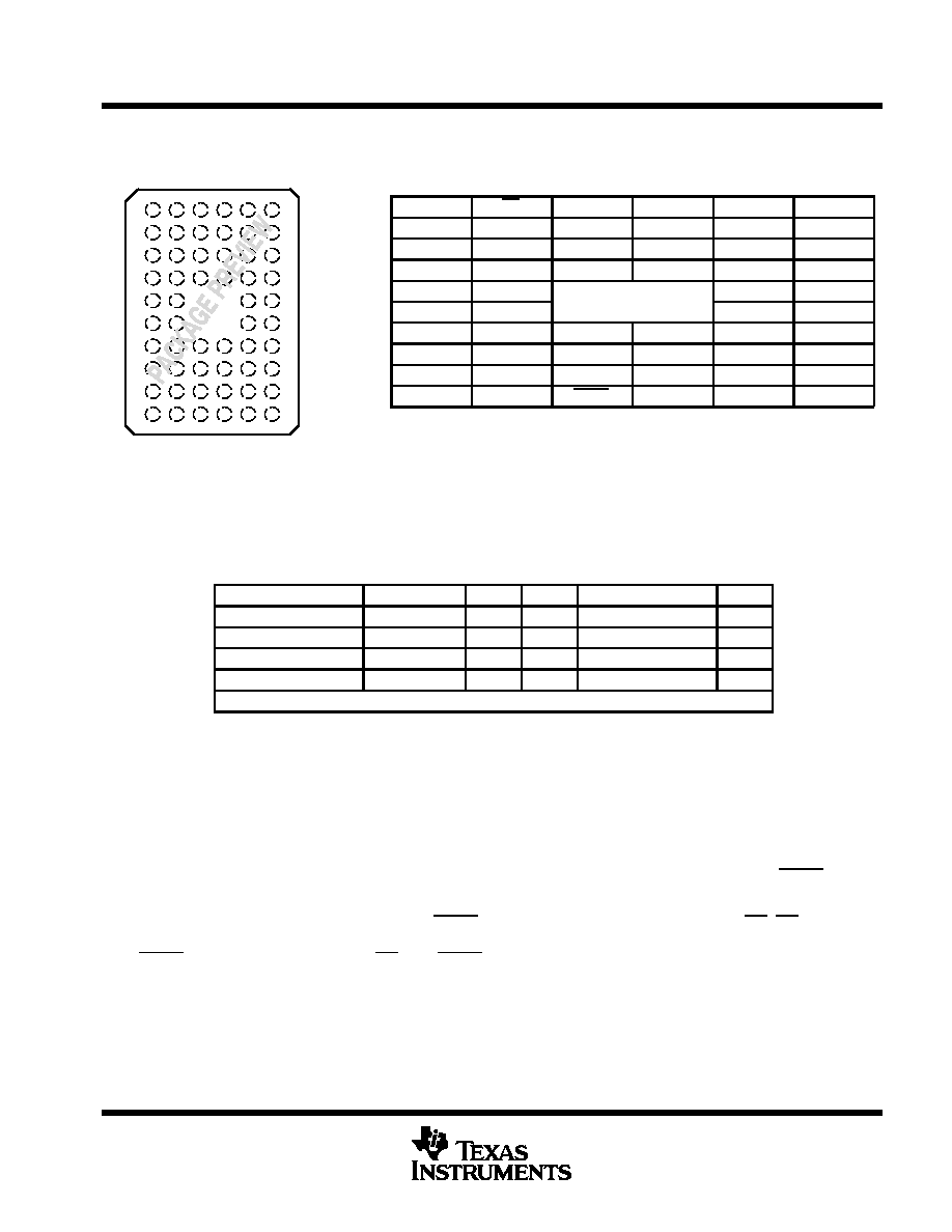
GQL PACKAGE
(TOP VIEW)
J
H
G
F
E
D
C
B
A
2
1
3
4
6
5
K
SN74GTLPH16927
18-BIT LVTTL-TO-GTLP BUS TRANSCEIVER
WITH SOURCE-SYNCHRONOUS CLOCK OUTPUTS
SCES413 OCTOBER 2002
4
POST OFFICE BOX 655303
·
DALLAS, TEXAS 75265
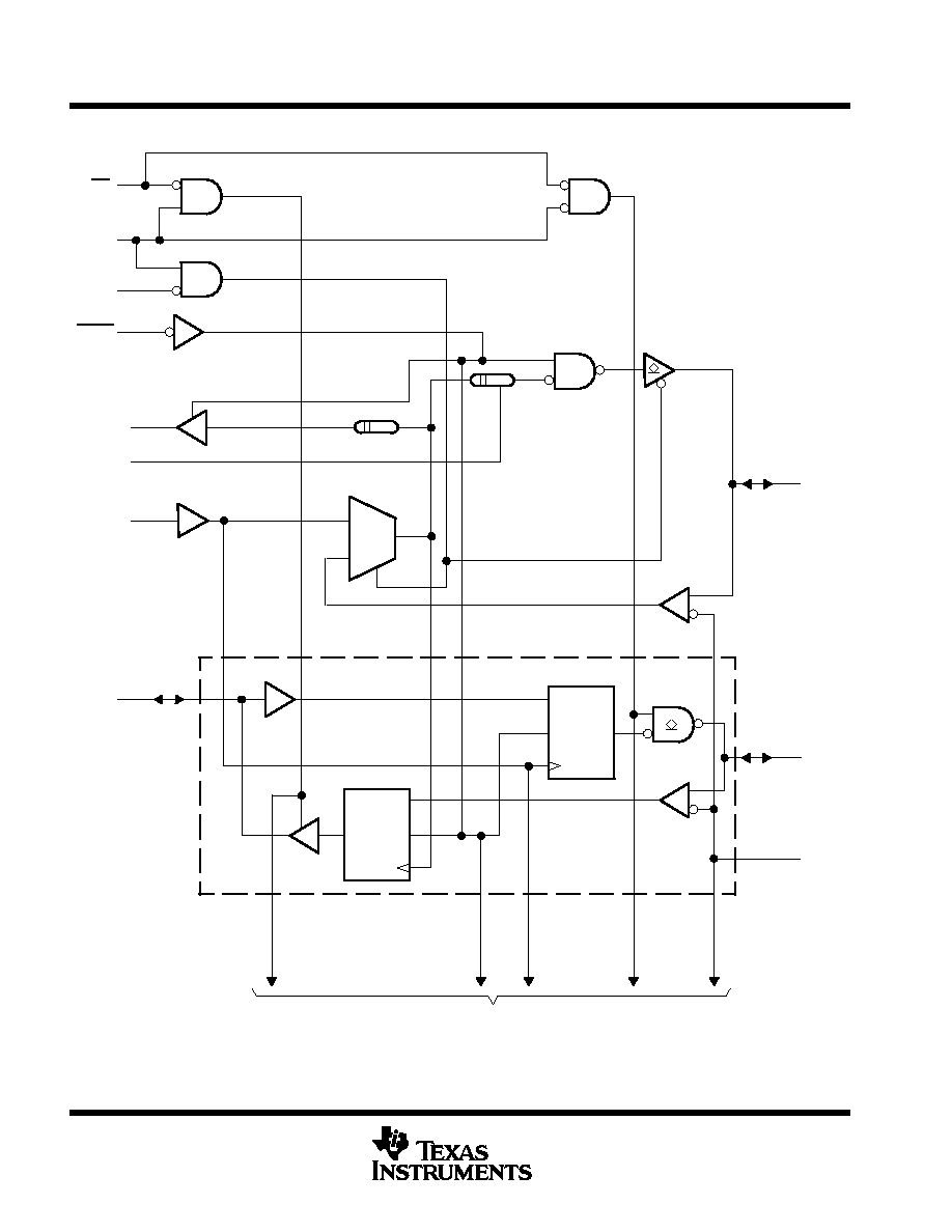
logic diagram (positive logic)
FSTA
SYSCLK
CLKOUT
SSCLK
27
56
29
30
MUX
OE
DIR
CMS
CKOE
A1
1D
C1
CLK
1D
C1
CLK
B1
VREF
2
1
35
28
3
50
54
Pin numbers shown are for the DGG and DGV packages.
One of Eighteen
Channels
To 17 Other Channels
SN74GTLPH16927
18-BIT LVTTL-TO-GTLP BUS TRANSCEIVER
WITH SOURCE-SYNCHRONOUS CLOCK OUTPUTS
SCES413 OCTOBER 2002
5
POST OFFICE BOX 655303
·
DALLAS, TEXAS 75265
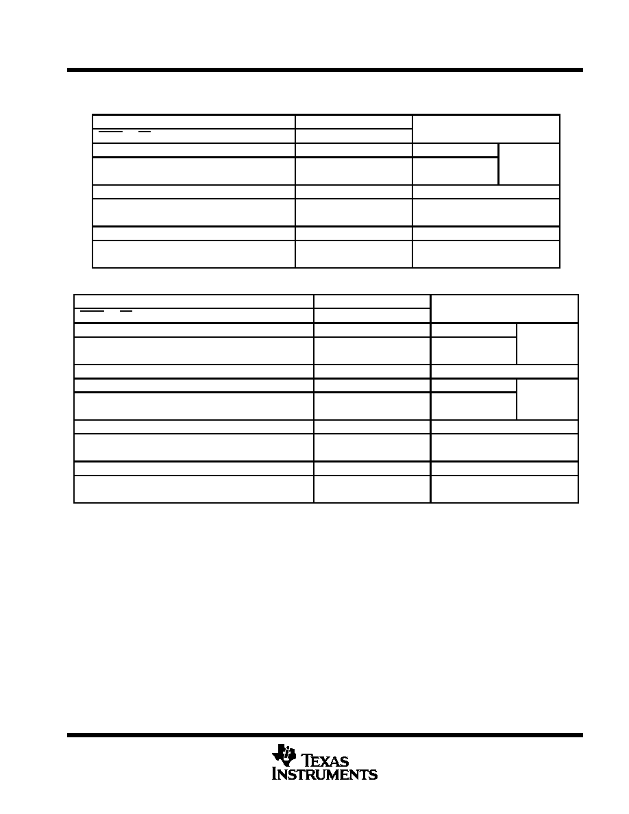
Function Tables
A-TO-B DIRECTION
INPUTS
OUTPUTS
MODE
CKOE
OE
CMS
DIR
SYSCLK
A
SSCLK
CLKOUT
B
MODE
L
L
X
L
H or L
X
SYSCLK
SYSCLK
B1
Latched storage of A
S
L
L
X
L
L
SYSCLK
SYSCLK
L
Clocked storage of A
Source
synchronous
L
L
X
L
H
SYSCLK
SYSCLK
H
Clocked storage of A
synchronous
L
H
X
L
X
X
SYSCLK
SYSCLK
Z
Data isolation
H
L
X
L
X
L
Z
Z
L
Transparent transmission of A
H
L
X
L
X
H
Z
Z
H
Transparent transmission of A
H
H
X
X
X
X
Z
Z
Z
Isolation
L
H
H
X
X
SYSCLK
SYSCLK
Z
Transmit SYSCLK
L
H
H
X
H or L
X
SYSCLK
SYSCLK
Z
Transmit SYSCLK
B-TO-A DIRECTION
INPUTS
OUTPUTS
MODE
CKOE
OE
CMS
DIR
SYSCLK
SSCLK
B
SSCLK
CLKOUT
A
MODE
L
L
L
H
X
H or L
X
Input
SSCLK
A1
Latched storage of B
S
L
L
L
H
X
L
Input
SSCLK
L
Clocked storage of B
Source
synchronous
L
L
L
H
X
H
Input
SSCLK
H
Clocked storage of B
synchronous
L
H
L
H
X
X
X
Input
SSCLK
Z
Data isolation
L
L
H
H
H or L
Output
X
SYSCLK
SYSCLK
A1
Latched storage of B
Cl
k
L
L
H
H
Output
L
SYSCLK
SYSCLK
L
Clocked storage of B
Clock
synchronous
L
L
H
H
Output
H
SYSCLK
SYSCLK
H
Clocked storage of B
synchronous
L
H
H
H
X
Output
X
SYSCLK
SYSCLK
Z
Data isolation
H
L
X
H
X
Output
L
Z
Z
L
Transparent transmission of B
H
L
X
H
X
Output
H
Z
Z
H
Transparent transmission of B
H
H
X
X
X
Output
X
Z
Z
Z
Isolation
L
H
L
X
X
X
Input
SSCLK
Z
Receive SSCLK
L
H
L
X
X
H or L
X
Input
SSCLK
Z
Receive SSCLK