
SN74CBT3251
1 OF 8 FET MULTIPLEXER/DEMULTIPLEXER
SCDS019L - MAY 1995 - REVISED JANUARY 2004
1
POST OFFICE BOX 655303
·
DALLAS, TEXAS 75265
D
5-
Switch Connection Between Two Ports
D
TTL-Compatible Input Levels
1
2
3
4
5
6
7
8
16
15
14
13
12
11
10
9
B4
B3
B2
B1
A
NC
OE
GND
V
CC
B5
B6
B7
B8
S0
S1
S2
D, DB, DBQ, OR PW PACKAGE
(TOP VIEW)
NC - No internal connection
RGY PACKAGE
(TOP VIEW)
1
16
8
9
2
3
4
5
6
7
15
14
13
12
11
10
B5
B6
B7
B8
S0
S1
B3
B2
B1
A
NC
OE
B4
S2
V
GND
CC
NC - No internal connection
description/ordering information
The SN74CBT3251 is a 1-of-8 high-speed TTL-compatible FET multiplexer/demultiplexer. The low on-state
resistance of the switch allows connections to be made with minimal propagation delay.
When output enable (OE) is low, the SN74CBT3251 is enabled. S0, S1, and S2 select one of the B outputs for
the A-input data.
ORDERING INFORMATION
TA
PACKAGE
ORDERABLE
PART NUMBER
TOP-SIDE
MARKING
QFN - RGY
Tape and reel
SN74CBT3251RGYR
CU251
SOIC - D
Tube
SN74CBT3251D
CBT3251
SOIC - D
Tape and reel
SN74CBT3251DR
CBT3251
-40
°
C to 85
°
C
SSOP - DB
Tape and reel
SN74CBT3251DBR
CU251
-40 C to 85 C
SSOP (QSOP) - DBQ
Tape and reel
SN74CBT3251DBQR
CU251
TSSOP - PW
Tube
SN74CBT3251PW
CU251
TSSOP - PW
Tape and reel
SN74CBT3251PWR
CU251
Package drawings, standard packing quantities, thermal data, symbolization, and PCB design
guidelines are available at www.ti.com/sc/package.
Copyright
2004, Texas Instruments Incorporated
PRODUCTION DATA information is current as of publication date.
Products conform to specifications per the terms of Texas Instruments
standard warranty. Production processing does not necessarily include
testing of all parameters.
Please be aware that an important notice concerning availability, standard warranty, and use in critical applications of
Texas Instruments semiconductor products and disclaimers thereto appears at the end of this data sheet.
SN74CBT3251
1 OF 8 FET MULTIPLEXER/DEMULTIPLEXER
SCDS019L - MAY 1995 - REVISED JANUARY 2004
2
POST OFFICE BOX 655303
·
DALLAS, TEXAS 75265
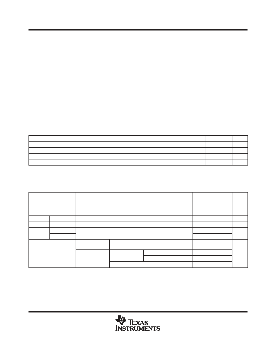
FUNCTION TABLE
(each multiplexer/demultiplexer)
INPUTS
FUNCTION
OE
S2
S1
S0
FUNCTION
L
L
L
L
A port = B1 port
L
L
L
H
A port = B2 port
L
L
H
L
A port = B3 port
L
L
H
H
A port = B4 port
L
H
L
L
A port = B5 port
L
H
L
H
A port = B6 port
L
H
H
L
A port = B7 port
L
H
H
H
A port = B8 port
H
X
X
X
Disconnect
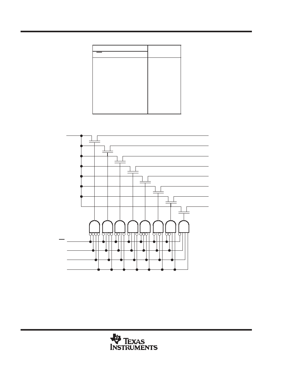
logic diagram (positive logic)
B5
B1
A
B2
B3
B4
B6
B7
B8
OE
S0
S1
S2
5
7
11
10
9
4
3
2
1
15
14
13
12
SN74CBT3251
1 OF 8 FET MULTIPLEXER/DEMULTIPLEXER
SCDS019L - MAY 1995 - REVISED JANUARY 2004
3
POST OFFICE BOX 655303
·
DALLAS, TEXAS 75265
absolute maximum ratings over operating free-air temperature range (unless otherwise noted)
Supply voltage range, V
CC
-0.5 V to 7 V
. . . . . . . . . . . . . . . . . . . . . . . . . . . . . . . . . . . . . . . . . . . . . . . . . . . . . . . . . .
Input voltage range, V
I
(see Note 1)
-0.5 V to 7 V
. . . . . . . . . . . . . . . . . . . . . . . . . . . . . . . . . . . . . . . . . . . . . . . . . .
Continuous channel current
128 mA
. . . . . . . . . . . . . . . . . . . . . . . . . . . . . . . . . . . . . . . . . . . . . . . . . . . . . . . . . . . . . .
Input clamp current, I
K
(V
I/O
< 0)
-50 mA
. . . . . . . . . . . . . . . . . . . . . . . . . . . . . . . . . . . . . . . . . . . . . . . . . . . . . . . . . .
Package thermal impedance,
JA
(see Note 2): D package
73
°
C/W
. . . . . . . . . . . . . . . . . . . . . . . . . . . . . . . . . . .
(see Note 2): DB package
82
°
C/W
. . . . . . . . . . . . . . . . . . . . . . . . . . . . . . . . .
(see Note 2): DBQ package
90
°
C/W
. . . . . . . . . . . . . . . . . . . . . . . . . . . . . . . .
(see Note 2): PW package
108
°
C/W
. . . . . . . . . . . . . . . . . . . . . . . . . . . . . . . .
(see Note 3): RGY package
39
°
C/W
. . . . . . . . . . . . . . . . . . . . . . . . . . . . . . . .
Storage temperature range, T
stg
-65
°
C to 150
°
C
. . . . . . . . . . . . . . . . . . . . . . . . . . . . . . . . . . . . . . . . . . . . . . . . . . .
Stresses beyond those listed under "absolute maximum ratings" may cause permanent damage to the device. These are stress ratings only, and
functional operation of the device at these or any other conditions beyond those indicated under "recommended operating conditions" is not
implied. Exposure to absolute-maximum-rated conditions for extended periods may affect device reliability.
NOTES:
1. The input and output negative-voltage ratings may be exceeded if the input and output clamp-current ratings are observed.
2. The package thermal impedance is calculated in accordance with JESD 51-7.
3. The package thermal impedance is calculated in accordance with JESD 51-5.
recommended operating conditions (see Note 4)
MIN
MAX
UNIT
VCC
Supply voltage
4
5.5
V
VIH
High-level control input voltage
2
V
VIL
Low-level control input voltage
0.8
V
TA
Operating free-air temperature
-40
85
°
C
NOTE 4: All unused control inputs of the device must be held at VCC or GND to ensure proper device operation. Refer to the TI application report,
Implications of Slow or Floating CMOS Inputs, literature number SCBA004.
electrical characteristics over recommended operating free-air temperature range (unless
otherwise noted)
PARAMETER
TEST CONDITIONS
MIN
TYP
MAX
UNIT
VIK
VCC = 4.5 V,
II = -18 mA
-1.2
V
II
VCC = 5.5 V,
VI = 5.5 V or GND
±
1
µ
A
ICC
VCC = 5.5 V,
IO = 0,
VI = VCC or GND
3
µ
A
ICC§
Control inputs
VCC = 5.5 V,
One input at 3.4 V,
Other inputs at VCC or GND
2.5
mA
Ci
Control inputs
VI = 3 V or 0
3.5
pF
Cio(OFF)
A port
VO = 3 V or 0,
OE = VCC
17.5
pF
Cio(OFF)
B port
VO = 3 V or 0,
OE = VCC
4
pF
VCC = 4 V,
TYP at VCC = 4 V
VI = 2.4 V,
II = 15 mA
14
20
ron¶
VI = 0
II = 64 mA
5
7
ron¶
VCC = 4.5 V
VI = 0
II = 30 mA
5
7
VCC = 4.5 V
VI = 2.4 V,
II = 15 mA
10
15
All typical values are at VCC = 5 V (unless otherwise noted), TA = 25
°
C.
§ This is the increase in supply current for each input that is at the specified TTL voltage level, rather than VCC or GND.
¶ Measured by the voltage drop between the A and the B terminals at the indicated current through the switch. On-state resistance is determined
by the lower of the voltages of the two (A or B) terminals.
SN74CBT3251
1 OF 8 FET MULTIPLEXER/DEMULTIPLEXER
SCDS019L - MAY 1995 - REVISED JANUARY 2004
4
POST OFFICE BOX 655303
·
DALLAS, TEXAS 75265
switching characteristics over recommended operating free-air temperature range, C
L
= 50 pF
(unless otherwise noted) (see Figure 1)
PARAMETER
FROM
(INPUT)
TO
(OUTPUT)
VCC = 4 V
VCC = 5 V
±
0.5 V
UNIT
PARAMETER
(INPUT)
(OUTPUT)
MIN
MAX
MIN
MAX
UNIT
tpd
A or B
B or A
0.35
0.25
ns
tpd
S
A
6
2
5.5
ns
ten
S
B
6.4
1.5
5.6
ns
ten
OE
A or B
6.4
1.6
5.8
ns
tdis
S
B
6.8
1.9
6.4
ns
tdis
OE
A or B
6
2.3
6.2
ns
The propagation delay is the calculated RC time constant of the typical on-state resistance of the switch and the specified load capacitance, when
driven by an ideal voltage source (zero output impedance).
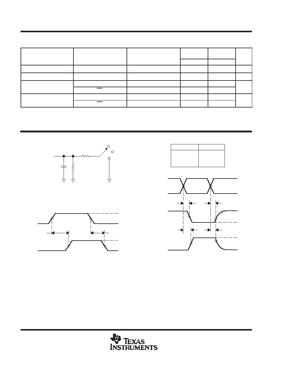
PARAMETER MEASUREMENT INFORMATION
VOH
VOL
From Output
Under Test
CL = 50 pF
(see Note A)
LOAD CIRCUIT
S1
7 V
Open
GND
500
500
tPLH
tPHL
Output
Control
Output
Waveform 1
S1 at 7 V
(see Note B)
Output
Waveform 2
S1 at Open
(see Note B)
tPZL
tPZH
tPLZ
tPHZ
3 V
0 V
VOH
VOL
0 V
VOL + 0.3 V
VOH - 0.3 V
0 V
Input
3 V
3.5 V
VOLTAGE WAVEFORMS
PROPAGATION DELAY TIMES
VOLTAGE WAVEFORMS
ENABLE AND DISABLE TIMES
Output
tpd
tPLZ/tPZL
tPHZ/tPZH
Open
7 V
Open
TEST
S1
NOTES: A. CL includes probe and jig capacitance.
B. Waveform 1 is for an output with internal conditions such that the output is low except when disabled by the output control.
Waveform 2 is for an output with internal conditions such that the output is high except when disabled by the output control.
C. All input pulses are supplied by generators having the following characteristics: PRR
10 MHz, ZO = 50
, tr
2.5 ns, tf
2.5 ns.
D. The outputs are measured one at a time with one transition per measurement.
E. tPLZ and tPHZ are the same as tdis.
F. tPZL and tPZH are the same as ten.
G. tPLH and tPHL are the same as tpd.
H. All parameters and waveforms are not applicable to all devices.
1.5 V
1.5 V
1.5 V
1.5 V
1.5 V
1.5 V
1.5 V
1.5 V
Figure 1. Load Circuit and Voltage Waveforms
PACKAGING INFORMATION
Orderable Device
Status
(1)
Package
Type
Package
Drawing
Pins Package
Qty
Eco Plan
(2)
Lead/Ball Finish
MSL Peak Temp
(3)
SN74CBT3251D
ACTIVE
SOIC
D
16
40
Green (RoHS &
no Sb/Br)
CU NIPDAU
Level-1-260C-UNLIM
SN74CBT3251DBLE
OBSOLETE
SSOP
DB
16
TBD
Call TI
Call TI
SN74CBT3251DBQR
ACTIVE
SSOP/
QSOP
DBQ
16
2500 Green (RoHS &
no Sb/Br)
CU NIPDAU
Level-2-260C-1YEAR
SN74CBT3251DBQRE4
ACTIVE
SSOP/
QSOP
DBQ
16
2500 Green (RoHS &
no Sb/Br)
CU NIPDAU
Level-2-260C-1YEAR
SN74CBT3251DBR
ACTIVE
SSOP
DB
16
2000 Green (RoHS &
no Sb/Br)
CU NIPDAU
Level-1-260C-UNLIM
SN74CBT3251DBRE4
ACTIVE
SSOP
DB
16
2000 Green (RoHS &
no Sb/Br)
CU NIPDAU
Level-1-260C-UNLIM
SN74CBT3251DE4
ACTIVE
SOIC
D
16
40
Green (RoHS &
no Sb/Br)
CU NIPDAU
Level-1-260C-UNLIM
SN74CBT3251DR
ACTIVE
SOIC
D
16
2500 Green (RoHS &
no Sb/Br)
CU NIPDAU
Level-1-260C-UNLIM
SN74CBT3251DRE4
ACTIVE
SOIC
D
16
2500 Green (RoHS &
no Sb/Br)
CU NIPDAU
Level-1-260C-UNLIM
SN74CBT3251PW
ACTIVE
TSSOP
PW
16
90
Green (RoHS &
no Sb/Br)
CU NIPDAU
Level-1-260C-UNLIM
SN74CBT3251PWE4
ACTIVE
TSSOP
PW
16
90
Green (RoHS &
no Sb/Br)
CU NIPDAU
Level-1-260C-UNLIM
SN74CBT3251PWLE
OBSOLETE
TSSOP
PW
16
TBD
Call TI
Call TI
SN74CBT3251PWR
ACTIVE
TSSOP
PW
16
2000 Green (RoHS &
no Sb/Br)
CU NIPDAU
Level-1-260C-UNLIM
SN74CBT3251PWRE4
ACTIVE
TSSOP
PW
16
2000 Green (RoHS &
no Sb/Br)
CU NIPDAU
Level-1-260C-UNLIM
SN74CBT3251RGYR
ACTIVE
QFN
RGY
16
1000 Green (RoHS &
no Sb/Br)
CU NIPDAU
Level-2-260C-1YEAR
(1)
The marketing status values are defined as follows:
ACTIVE: Product device recommended for new designs.
LIFEBUY: TI has announced that the device will be discontinued, and a lifetime-buy period is in effect.
NRND: Not recommended for new designs. Device is in production to support existing customers, but TI does not recommend using this part in
a new design.
PREVIEW: Device has been announced but is not in production. Samples may or may not be available.
OBSOLETE: TI has discontinued the production of the device.
(2)
Eco
Plan
-
The
planned
eco-friendly
classification:
Pb-Free
(RoHS)
or
Green
(RoHS
&
no
Sb/Br)
-
please
check
http://www.ti.com/productcontent
for the latest availability information and additional product content details.
TBD: The Pb-Free/Green conversion plan has not been defined.
Pb-Free (RoHS): TI's terms "Lead-Free" or "Pb-Free" mean semiconductor products that are compatible with the current RoHS requirements
for all 6 substances, including the requirement that lead not exceed 0.1% by weight in homogeneous materials. Where designed to be soldered
at high temperatures, TI Pb-Free products are suitable for use in specified lead-free processes.
Green (RoHS & no Sb/Br): TI defines "Green" to mean Pb-Free (RoHS compatible), and free of Bromine (Br) and Antimony (Sb) based flame
retardants (Br or Sb do not exceed 0.1% by weight in homogeneous material)
(3)
MSL, Peak Temp. -- The Moisture Sensitivity Level rating according to the JEDEC industry standard classifications, and peak solder
temperature.
Important Information and Disclaimer:The information provided on this page represents TI's knowledge and belief as of the date that it is
provided. TI bases its knowledge and belief on information provided by third parties, and makes no representation or warranty as to the
accuracy of such information. Efforts are underway to better integrate information from third parties. TI has taken and continues to take
reasonable steps to provide representative and accurate information but may not have conducted destructive testing or chemical analysis on
PACKAGE OPTION ADDENDUM
www.ti.com
30-Aug-2005
Addendum-Page 1