SN74CBT16244C
16 BIT FET BUS SWITCH
5 V BUS SWITCH WITH 2 V UNDERSHOOT PROTECTION
SCDS134A - SEPTEMBER 2003 - REVISED OCTOBER 2003
1
POST OFFICE BOX 655303
·
DALLAS, TEXAS 75265
D
Member of the Texas Instruments
Widebus
Family
D
Undershoot Protection for Off-Isolation on
A and B Ports Up To -2 V
D
Bidirectional Data Flow, With Near-Zero
Propagation Delay
D
Low ON-State Resistance (r
on
)
Characteristics (r
on
= 3
Typical)
D
Low Input/Output Capacitance Minimizes
Loading and Signal Distortion
(C
io(OFF)
= 5.5 pF Typical)
D
Data and Control Inputs Provide
Undershoot Clamp Diodes
D
Low Power Consumption
(I
CC
= 3
µ
A Max)
D
V
CC
Operating Range From 4 V to 5.5 V
D
Data I/Os Support 0 to 5-V Signaling Levels
(0.8-V, 1.2-V, 1.5-V, 1.8-V, 2.5-V, 3.3-V, 5-V)
D
Control Inputs Can Be Driven by TTL or
5-V/3.3-V CMOS Outputs
D
I
off
Supports Partial-Power-Down Mode
Operation
D
Latch-Up Performance Exceeds 100 mA Per
JESD 78, Class II
D
ESD Performance Tested Per JESD 22
- 2000-V Human-Body Model
(A114-B, Class II)
- 1000-V Charged-Device Model (C101)
D
Supports Both Digital and Analog
Applications: PCI Interface, Memory
Interleaving, Bus Isolation, Low-Distortion
Signal Gating
description/ordering information
ORDERING INFORMATION
TA
PACKAGE
ORDERABLE
PART NUMBER
TOP-SIDE
MARKING
SSOP - DL
Tube
SN74CBT16244CDL
CBT16244C
SSOP - DL
Tape and reel
SN74CBT16244CDLR
CBT16244C
-40
°
C to 85
°
C
TSSOP - DGG
Tube
SN74CBT16244CDGG
CBT16244C
-40 C to 85 C
TSSOP - DGG
Tape and reel
SN74CBT16244CDGGR
CBT16244C
TVSOP - DGV
Tape and reel
SN74CBT16244CDGVR
CY244C
Package drawings, standard packing quantities, thermal data, symbolization, and PCB design
guidelines are available at www.ti.com/sc/package.
Copyright
2003, Texas Instruments Incorporated
1
2
3
4
5
6
7
8
9
10
11
12
13
14
15
16
17
18
19
20
21
22
23
24
48
47
46
45
44
43
42
41
40
39
38
37
36
35
34
33
32
31
30
29
28
27
26
25
1OE
1B1
1B2
GND
1B3
1B4
V
CC
2B1
2B2
GND
2B3
2B4
3B1
3B2
GND
3B3
3B4
V
CC
4B1
4B2
GND
4B3
4B4
4OE
2OE
1A1
1A2
GND
1A3
1A4
V
CC
2A1
2A2
GND
2A3
2A4
3A1
3A2
GND
3A3
3A4
V
CC
4A1
4A2
GND
4A3
4A4
3OE
DGG, DGV, OR DL PACKAGE
(TOP VIEW)
Please be aware that an important notice concerning availability, standard warranty, and use in critical applications of
Texas Instruments semiconductor products and disclaimers thereto appears at the end of this data sheet.
PRODUCTION DATA information is current as of publication date.
Products conform to specifications per the terms of Texas Instruments
standard warranty. Production processing does not necessarily include
testing of all parameters.
Widebus is a trademark of Texas Instruments.

SN74CBT16244C
16 BIT FET BUS SWITCH
5 V BUS SWITCH WITH 2 V UNDERSHOOT PROTECTION
SCDS134A - SEPTEMBER 2003 - REVISED OCTOBER 2003
2
POST OFFICE BOX 655303
·
DALLAS, TEXAS 75265
description/ordering information (continued)
The SN74CBT16244C is a high-speed TTL-compatible FET bus switch with low ON-state resistance (r
on
),
allowing for minimal propagation delay. Active Undershoot-Protection Circuitry on the A and B ports of the
SN74CBT16244C provides protection for undershoot up to -2 V by sensing an undershoot event and ensuring
that the switch remains in the proper OFF state.
The SN74CBT16244C is organized as four 4-bit bus switches with separate output-enable (1OE, 2OE, 3OE,
4OE) inputs. It can be used as four 4-bit bus switches, two 8-bit bus switches, or as one 16-bit bus switch. When
OE is low, the associated 4-bit bus switch is ON, and the A port is connected to the B port, allowing bidirectional
data flow between ports. When OE is high, the associated 4-bit bus switch is OFF, and the high-impedance state
exists between the A and B ports.
This device is fully specified for partial-power-down applications using I
off
. The I
off
feature ensures that
damaging current will not backflow through the device when it is powered down. The device has isolation during
power off.
To ensure the high-impedance state during power up or power down, OE should be tied to V
CC
through a pullup
resistor; the minimum value of the resistor is determined by the current-sinking capability of the driver.
FUNCTION TABLE
(each 4-bit bus switch)
INPUT
INPUT/OUTPUT
FUNCTION
INPUT
OE
INPUT/OUTPUT
A
FUNCTION
L
B
A port = B port
H
Z
Disconnect
logic diagram (positive logic)
1A1
SW
1B1
1A4
1OE
SW
1B4
3A1
SW
3B1
3A4
3OE
SW
3B4
47
43
1
36
32
25
2
6
13
17
2A1
SW
2B1
2A4
2OE
SW
2B4
4A1
SW
4B1
4A4
4OE
SW
4B4
41
37
48
30
26
24
8
12
19
23
SN74CBT16244C
16 BIT FET BUS SWITCH
5 V BUS SWITCH WITH 2 V UNDERSHOOT PROTECTION
SCDS134A - SEPTEMBER 2003 - REVISED OCTOBER 2003
3
POST OFFICE BOX 655303
·
DALLAS, TEXAS 75265
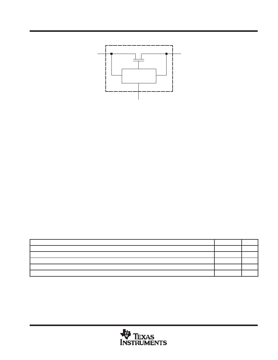
simplified schematic, each FET switch (SW)
A
EN
B
EN is the internal enable signal applied to the switch.
Undershoot
Protection Circuit
absolute maximum ratings over operating free-air temperature range (unless otherwise noted)
Supply voltage range, V
CC
-0.5 V to 7 V
. . . . . . . . . . . . . . . . . . . . . . . . . . . . . . . . . . . . . . . . . . . . . . . . . . . . . . . . . .
Control input voltage range, V
IN
(see Notes 1 and 2)
-0.5 V to 7 V
. . . . . . . . . . . . . . . . . . . . . . . . . . . . . . . . . . .
Switch I/O voltage range, V
I/O
(see Notes 1, 2, and 3)
-0.5 V to 7 V
. . . . . . . . . . . . . . . . . . . . . . . . . . . . . . . . . .
Control input clamp current, I
IK
(V
IN
< 0)
-50 mA
. . . . . . . . . . . . . . . . . . . . . . . . . . . . . . . . . . . . . . . . . . . . . . . . . . .
I/O port clamp current, I
I/OK
(V
I/O
< 0)
-50 mA
. . . . . . . . . . . . . . . . . . . . . . . . . . . . . . . . . . . . . . . . . . . . . . . . . . . . .
ON-state switch current, I
I/O
(see Note 4)
±
128 mA
. . . . . . . . . . . . . . . . . . . . . . . . . . . . . . . . . . . . . . . . . . . . . . . . .
Continuous current through V
CC
or GND terminals
±
100 mA
. . . . . . . . . . . . . . . . . . . . . . . . . . . . . . . . . . . . . . . . .
Package thermal impedance,
JA
(see Note 5): DGG package
70
°
C/W
. . . . . . . . . . . . . . . . . . . . . . . . . . . . . . .
DGV package
58
°
C/W
. . . . . . . . . . . . . . . . . . . . . . . . . . . . . . . .
DL package
63
°
C/W
. . . . . . . . . . . . . . . . . . . . . . . . . . . . . . . . .
Storage temperature range, T
stg
-65
°
C to 150
°
C
. . . . . . . . . . . . . . . . . . . . . . . . . . . . . . . . . . . . . . . . . . . . . . . . . . .
Stresses beyond those listed under "absolute maximum ratings" may cause permanent damage to the device. These are stress ratings only, and
functional operation of the device at these or any other conditions beyond those indicated under "recommended operating conditions" is not
implied. Exposure to absolute-maximum-rated conditions for extended periods may affect device reliability.
NOTES:
1. All voltages are with respect to ground unless otherwise specified.
2. The input and output voltage ratings may be exceeded if the input and output clamp-current ratings are observed.
3. VI and VO are used to denote specific conditions for VI/O.
4. II and IO are used to denote specific conditions for II/O.
5. The package thermal impedance is calculated in accordance with JESD 51-7.
recommended operating conditions (see Note 6)
MIN
MAX
UNIT
VCC
Supply voltage
4
5.5
V
VIH
High-level control input voltage
2
5.5
V
VIL
Low-level control input voltage
0
0.8
V
VI/O
Data input/output voltage
0
5.5
V
TA
Operating free-air temperature
-40
85
°
C
NOTE 6: All unused control inputs of the device must be held at VCC or GND to ensure proper device operation. Refer to the TI application report,
Implications of Slow or Floating CMOS Inputs, literature number SCBA004.
SN74CBT16244C
16 BIT FET BUS SWITCH
5 V BUS SWITCH WITH 2 V UNDERSHOOT PROTECTION
SCDS134A - SEPTEMBER 2003 - REVISED OCTOBER 2003
4
POST OFFICE BOX 655303
·
DALLAS, TEXAS 75265
electrical characteristics over recommended operating free-air temperature range (unless
otherwise noted)
PARAMETER
TEST CONDITIONS
MIN
TYP
MAX
UNIT
VIK
Control inputs
VCC = 4.5 V,
IIN = -18 mA
-1.8
V
VIKU
Data inputs
VCC = 5 V,
0 mA
>
II
-50 mA,
VIN = VCC or GND,
Switch OFF
-2
V
IIN
Control inputs
VCC = 5.5 V,
VIN = VCC or GND
±
1
µ
A
IOZ
VCC = 5.5 V,
VO = 0 to 5.5 V,
VI = 0,
Switch OFF,
VIN = VCC or GND
±
10
µ
A
Ioff
VCC = 0,
VO = 0 to 5.5 V,
VI = 0
10
µ
A
ICC
VCC = 5.5 V,
II/O = 0,
VIN = VCC or GND,
Switch ON or OFF
3
µ
A
ICC§
Control inputs
VCC = 5.5 V,
One input at 3.4 V,
Other inputs at VCC or GND
2.5
mA
Cin
Control inputs
VIN = 3 V or 0
3.5
pF
Cio(OFF)
VI/O = 3 V or 0,
Switch OFF,
VIN = VCC or GND
5.5
pF
Cio(ON)
VI/O = 3 V or 0,
Switch ON,
VIN = VCC or GND
14
pF
VCC = 4 V,
TYP at VCC = 4 V
VI = 2.4 V,
IO = -15 mA
8
12
ron¶
VI = 0
IO = 64 mA
3
6
ron¶
VCC = 4.5 V
VI = 0
IO = 30 mA
3
6
VCC = 4.5 V
VI = 2.4 V,
IO = -15 mA
5
10
VIN and IIN refer to control inputs. VI, VO, II, and IO refer to data pins.
All typical values are at VCC = 5 V (unless otherwise noted), TA = 25
°
C.
For I/O ports, the parameter IOZ includes the input leakage current.
§ This is the increase in supply current for each input that is at the specified voltage level, rather than VCC or GND.
¶ Measured by the voltage drop between the A and B terminals at the indicated current through the switch. ON-state resistance is determined by
the lower of the voltages of the two (A or B) terminals.
switching characteristics over recommended operating free-air temperature range (unless
otherwise noted) (see Figure 3)
PARAMETER
FROM
(INPUT)
TO
(OUTPUT)
VCC = 4 V
VCC = 5 V
±
0.5 V
UNIT
PARAMETER
(INPUT)
(OUTPUT)
MIN
MAX
MIN
MAX
UNIT
tpd#
A or B
B or A
0.24
0.15
ns
ten
OE
A or B
5.1
1.5
4.7
ns
tdis
OE
A or B
5.2
1.5
5.4
ns
# The propagation delay is the calculated RC time constant of the typical ON-state resistance of the switch and the specified load capacitance,
when driven by an ideal voltage source (zero output impedance).
SN74CBT16244C
16 BIT FET BUS SWITCH
5 V BUS SWITCH WITH 2 V UNDERSHOOT PROTECTION
SCDS134A - SEPTEMBER 2003 - REVISED OCTOBER 2003
5
POST OFFICE BOX 655303
·
DALLAS, TEXAS 75265
undershoot characteristics (see Figures 1 and 2)
PARAMETER
TEST CONDITIONS
MIN
TYP
MAX
UNIT
VOUTU
VCC = 5.5 V,
Switch OFF,
VIN = VCC or GND
2
VOH-0.3
V
All typical values are at VCC = 5 V (unless otherwise noted), TA = 25
°
C.
Figure 1. Device Test Setup
50
VS
VCC
11 V
100 k
100 k
10 pF
DUT
Input
Generator
Ax
Bx
Figure 2. Transient Input Voltage (V
I
) and Output
Voltage (V
OUTU
) Waveforms
(Switch OFF)
-2 V
5.5 V
10 %
20 ns
10 %
90 %
90 %
2 ns
2 ns
VOH - 0.3
VOH
Output
(VOUTU)
Input
(Open
Socket)