
SN74BCT651
OCTAL BUS TRANSCEIVER AND REGISTER
WITH 3-STATE OUTPUTS
SCBS054A AUGUST 1990 REVISED NOVEMBER 1993
Copyright
©
1993, Texas Instruments Incorporated
21
POST OFFICE BOX 655303
·
DALLAS, TEXAS 75265
·
State-of-the-Art BiCMOS Design
Significantly Reduces I
CCZ
·
Independent Registers for A and B Buses
·
Multiplexed Real-Time and Stored Data
·
Inverting Data Paths
·
Power-Up High-Impedance Mode
·
Package Options Include Plastic
Small-Outline (DW) Packages and Standard
Plastic 300-mil DIPs (NT)
description
This SN74BCT651 consists of bus transceiver
circuits, D-type flip-flops, and control circuitry
arranged for multiplexed transmission of data
directly from the data bus or from the internal
storage registers. Output-enable (OEAB and OEBA) inputs are provided to control the transceiver functions.
The select-control (SAB and SBA) inputs are provided to select whether real-time or stored data is transferred.
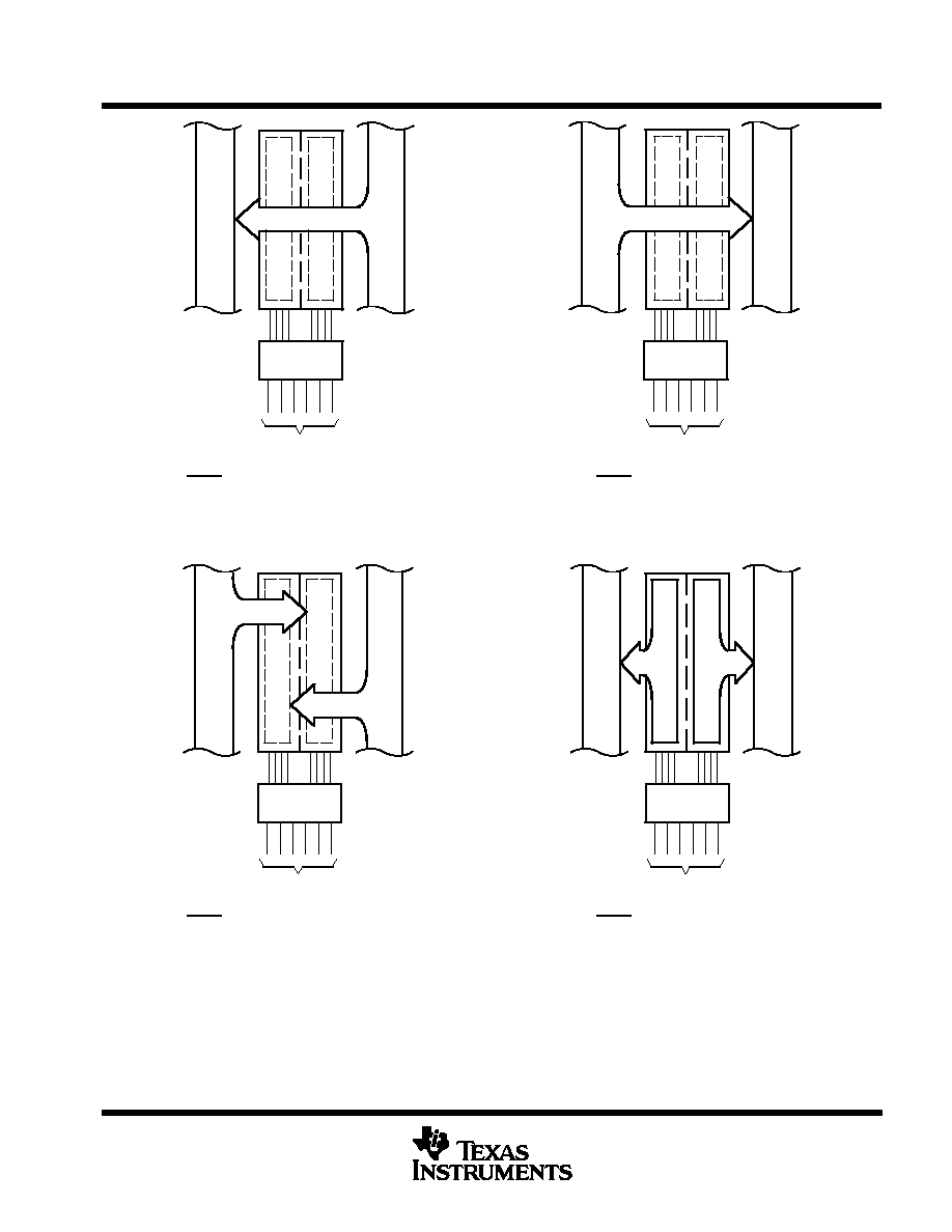
A low input level selects real-time data, and a high input level selects stored data. Figure 1 illustrates the four
fundamental bus-management functions that can be performed with the SN74BCT651.
Data on the A or B bus, or both, can be stored in the internal D flip-flops by low-to-high transitions at the
appropriate clock (CLKAB or CLKBA) inputs regardless of the select- or enable-control pins. When SAB and
SBA are in the real-time transfer mode, it is also possible to store data without using the internal D-type flip-flops
by simultaneously enabling OEAB and OEBA. In this configuration, each output reinforces its input. Thus, when
all the other data sources to the two sets of bus lines are at high impedance, each set will remain at its last state.
The SN74BCT651 is characterized for operation from 0
°
C to 70
°
C.
FUNCTION TABLE
INPUTS
DATA I/O
OPERATION OR FUNCTION
OEAB
OEBA
CLKAB
CLKBA
SAB
SBA
A1 THRU A8
B1 THRU B8
OPERATION OR FUNCTION
L
H
H or L
H or L
X
X
Input
Input
Isolation
L
H
X
X
Input
Input
Store A and B data
X
H
H or L
X
X
Input
Unspecified
Store A, hold B
H
H
X
X
Input
Output
Store A in both registers
L
X
H or L
X
X
Unspecified
Input
Hold A, store B
L
L
X
X
Output
Input
Store B in both registers
L
L
X
X
X
L
Output
Input
Real-time B data to A bus
L
L
X
H or L
X
H
Output
Input
Stored B data to A bus
H
H
X
X
L
X
Input
Output
Real-time A data to B bus
H
H
H or L
X
H
X
Input
Output
Stored A data to B bus
H
L
H or L
H or L
H
H
Output
Output
Stored A data to B bus and
stored B data to A bus
The data output functions may be enabled or disabled by various signals at the OEAB or OEBA inputs. Data input functions are always enabled,
i.e., data at the bus pins will be stored on every low-to-high transition on the clock inputs.
When select control is low, clocks can occur simultaneously so long as allowances are made for propagation delays from A to B (B to A) plus
setup and hold times. When select control is high, clocks must be staggered in order to load both registers.
1
2
3
4
5
6
7
8
9
10
11
12
24
23
22
21
20
19
18
17
16
15
14
13
CLKAB
SAB
OEAB
A1
A2
A3
A4
A5
A6
A7
A8
GND
V
CC
CLKBA
SBA
OEBA
B1
B2
B3
B4
B5
B6
B7
B8
DW OR NT PACKAGE
(TOP VIEW)
PRODUCTION DATA information is current as of publication date.
Products conform to specifications per the terms of Texas Instruments
standard warranty. Production processing does not necessarily include
testing of all parameters.
SN74BCT651
OCTAL BUS TRANSCEIVER AND REGISTER
WITH 3-STATE OUTPUTS
SCBS054A AUGUST 1990 REVISED NOVEMBER 1993
22
POST OFFICE BOX 655303
·
DALLAS, TEXAS 75265
BUS A
BUS B
BUS A
BUS B
3
21
1
23
2
22
3
21
1
23
2
22
OEAB
OEAB
CLKAB
CLKBA
SAB
SBA
OEAB
OEAB
CLKAB
CLKBA
SAB
SBA
L
L
X
X
X
L
H
H
X
X
L
X
REAL-TIME TRANSFER BUS B TO BUS A
REAL-TIME TRANSFER BUS A TO BUS B
BUS A
BUS B
BUS A
BUS B
3
21
1
23
2
22
21
3
1
23
2
22
OEAB
OEAB
CLKAB
CLKBA
SAB
SBA
OEAB
OEAB
CLKAB
CLKBA
SAB
SBA
X
H
X
X
X
H
L
H or L
H or L
H
H
L
X
X
X
X
L
H
X
X
STORAGE FROM A,B, OR A AND B
TRANSFER STORED DATA TO A AND/OR B
Figure 1. Bus-Management Functions
SN74BCT651
OCTAL BUS TRANSCEIVER AND REGISTER
WITH 3-STATE OUTPUTS
SCBS054A AUGUST 1990 REVISED NOVEMBER 1993
23
POST OFFICE BOX 655303
·
DALLAS, TEXAS 75265
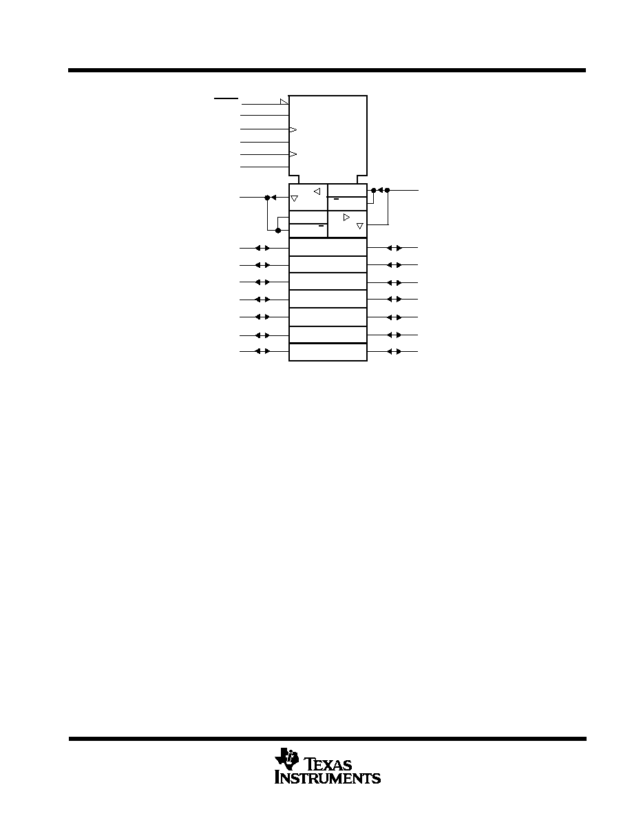
logic symbol
1
1
2
A1
4
A2
5
A3
6
A4
7
A5
A6
A7
A8
9
OEAB
B1
B2
B3
B4
B5
B6
B7
B8
10
22
21
11
23
13
14
15
3
EN1 [BA]
EN2 [AB]
1
4D
6D
1
7
CLKBA
SBA
CLKAB
SAB
8
1
16
17
18
19
20
2
C4
G5
C6
G7
OEBA
7
5
5
1
This symbol is in accordance with ANSI/IEEE Std 91-1984 and IEC Publication 617-12.
SN74BCT651
OCTAL BUS TRANSCEIVER AND REGISTER
WITH 3-STATE OUTPUTS
SCBS054A AUGUST 1990 REVISED NOVEMBER 1993
24
POST OFFICE BOX 655303
·
DALLAS, TEXAS 75265
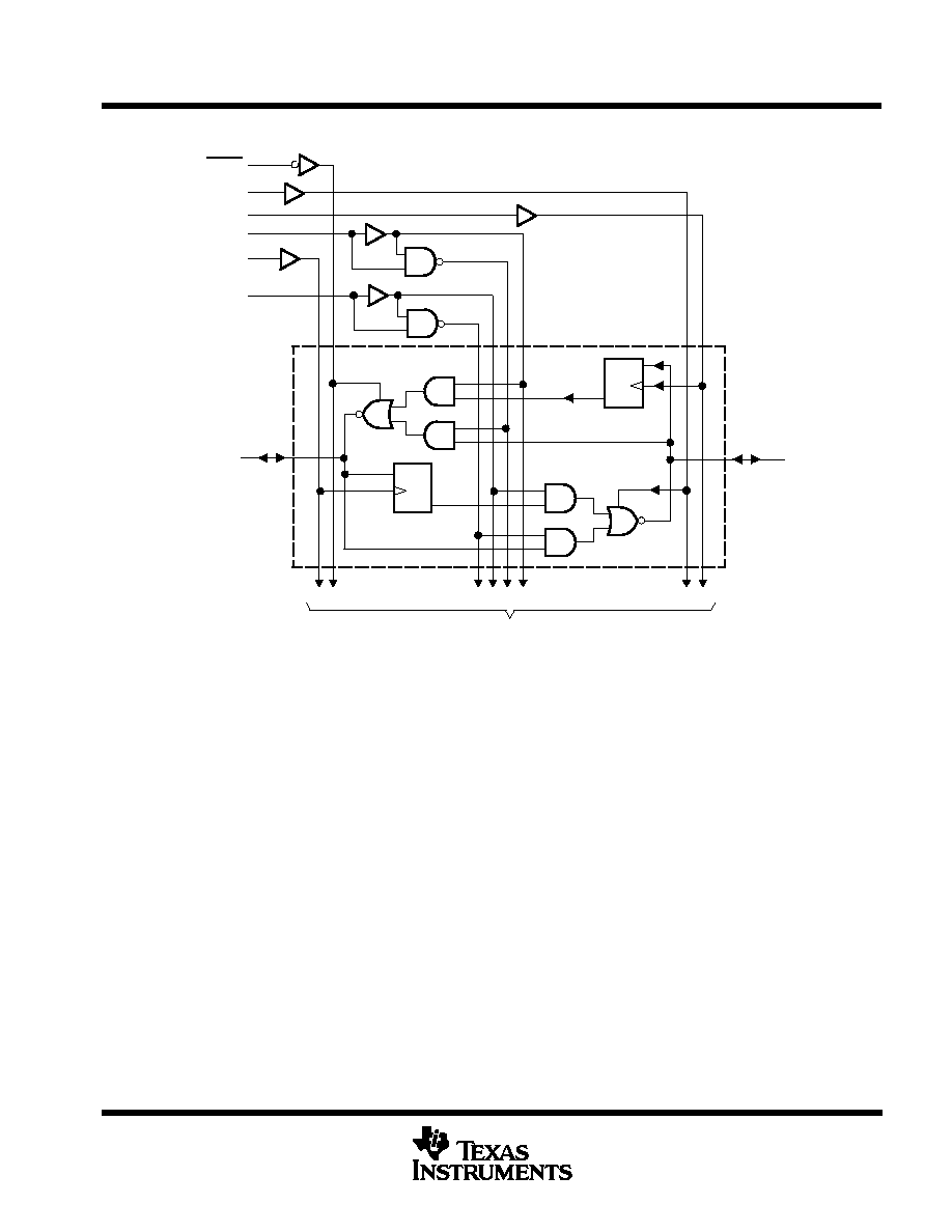
logic diagram
A1
2
3
4
B1
SBA
SAB
20
23
1
22
21
1D
1D
C1
C1
OEAB
CLKBA
CLKAB
OEBA
To Seven Other Channels
One of Eight
Channels
absolute maximum ratings over operating free-air temperature range (unless otherwise noted)
Supply voltage range, V
CC
0.5 V to 7 V
. . . . . . . . . . . . . . . . . . . . . . . . . . . . . . . . . . . . . . . . . . . . . . . . . . . . . . . . . .
Input voltage range: Control inputs (see Note 1)
0.5 V to 7 V
. . . . . . . . . . . . . . . . . . . . . . . . . . . . . . . . . . . . . . . .
I/O ports (see Note 1)
0.5 V to 5.5 V
. . . . . . . . . . . . . . . . . . . . . . . . . . . . . . . . . . . . . . . . . .
Voltage range applied to any output in the disabled or power-off state, V
O
0.5 V to 5.5 V
. . . . . . . . . . . . . . .
Voltage range applied to any output in the high state, V
O
0.5 V to V
CC
. . . . . . . . . . . . . . . . . . . . . . . . . . . . . . .
Current into any output in the low state
128 mA
. . . . . . . . . . . . . . . . . . . . . . . . . . . . . . . . . . . . . . . . . . . . . . . . . . . . .
Operating free-air temperature range
0
°
C to 70
°
C
. . . . . . . . . . . . . . . . . . . . . . . . . . . . . . . . . . . . . . . . . . . . . . . . . . .
Storage temperature range
65
°
C to 150
°
C
. . . . . . . . . . . . . . . . . . . . . . . . . . . . . . . . . . . . . . . . . . . . . . . . . . . . . . . .
Stresses beyond those listed under "absolute maximum ratings" may cause permanent damage to the device. These are stress ratings only, and
functional operation of the device at these or any other conditions beyond those indicated under "recommended operating conditions" is not
implied. Exposure to absolute-maximum-rated conditions for extended periods may affect device reliability.
NOTE 1: The input and output voltage ratings may be exceeded if the input and output current ratings are observed.

SN74BCT651
OCTAL BUS TRANSCEIVER AND REGISTER
WITH 3-STATE OUTPUTS
SCBS054A AUGUST 1990 REVISED NOVEMBER 1993
25
POST OFFICE BOX 655303
·
DALLAS, TEXAS 75265
recommended operating conditions
MIN
NOM
MAX
UNIT
VCC
Supply voltage
4.5
5
5.5
V
VIH
High-level input voltage
2
V
VIL
Low-level input voltage
0.8
V
IIK
Input clamp current
18
mA
IOH
High-level output current
15
mA
IOL
Low-level output current
64
mA
TA
Operating free-air temperature
0
70
°
C
electrical characteristics over recommended operating free-air temperature range (unless
otherwise noted)
PARAMETER
TEST CONDITIONS
MIN
TYP
MAX
UNIT
VIK
VCC = 4.5 V,
II = 18 mA
1.2
V
VCC = 4 5 V
IOH = 3 mA
2.4
3.3
VOH
VCC = 4.5 V
IOH = 15 mA
2
3.1
V
VCC = 4.75 V,
IOH = 3 mA
2.7
VOL
VCC = 4.5 V,
IOL = 64 mA
0.42
0.55
V
II
A or B port
VCC = 5 5 V
VI = 5 5 V
1
mA
II
Control inputs
VCC = 5.5 V,
VI = 5.5 V
1
mA
IIH
A or B port
VCC = 5 5 V
VI = 2 7 V
70
µ
A
IIH
Control inputs
VCC = 5.5 V,
VI = 2.7 V
20
µ
A
I
A or B port
VCC = 5 5 V
VI = 0 5 V
0.7
mA
IIL
Control inputs
VCC = 5.5 V,
VI = 0.5 V
0.7
mA
IOS§
VCC = 5.5 V,
VO = 0
100
225
mA
ICCL
A or B port
VCC = 5.5 V,
VI = GND
39
62
mA
ICCH
A or B port
VCC = 5.5 V,
VI = 4.5 V
8
13
mA
ICCZ
A or B port
VCC = 5.5 V,
VI = GND
10
16
mA
Ci
Control inputs
VCC = 5 V,
VI = 2.5 V or 0.5 V
5.5
pF
Cio
A or B port
VCC = 5 V,
VO = 2.5 V or 0.5 V
11
pF
All typical values are at VCC = 5 V, TA = 25
°
C.
For I/O ports, the parameters IIH and IIL include the off-state output current.
§ Not more than one output should be tested at a time, and the duration of the test should not exceed one second.
timing requirements over recommended ranges of supply voltage and operating free-air
temperature (unless otherwise noted)
VCC = 5 V,
TA = 25
°
C
MIN
MAX
UNIT
MIN
MAX
fclock
Clock frequency
0
85
0
85
MHz
t
Pulse duration
CLK high
4.8
4.8
ns
tw
Pulse duration
CLK low
7
7
ns
tsu
Setup time, A or B before CLK
6
6
ns
th
Hold time, A or B after CLK
1
1
ns