SN74AVCAH164245
16 BIT DUAL SUPPLY BUS TRANSCEIVER
WITH CONFIGURABLE VOLTAGE TRANSLATION AND 3 STATE OUTPUTS
SCES396A - JULY 2002 - REVISED MAY 2004
1
POST OFFICE BOX 655303
·
DALLAS, TEXAS 75265
D
Member of the Texas Instruments
Widebus
Family
D
DOC
Circuitry Dynamically Changes
Output Impedance, Resulting in Noise
Reduction Without Speed Degradation
D
Dynamic Drive Capability Is Equivalent to
Standard Outputs With I
OH
and I
OL
of
±
24 mA at 2.5-V V
CC
D
Control Inputs V
IH
/V
IL
Levels are
Referenced to V
CCA
Voltage
D
If Either V
CC
Input Is at GND, Both Ports
Are in the High-Impedance State
D
Overvoltage-Tolerant Inputs/Outputs Allow
Mixed-Voltage-Mode Data Communications
D
I
off
Supports Partial-Power-Down Mode
Operation
D
Fully Configurable Dual-Rail Design Allows
Each Port to Operate Over the Full 1.4-V to
3.6-V Power-Supply Range
D
Bus Hold on Data Inputs Eliminates the
Need for External Pullup / Pulldown
Resistors
D
Latch-Up Performance Exceeds 100 mA Per
JESD 78, Class II
D
ESD Protection Exceeds JESD 22
- 2000-V Human-Body Model (A114-A)
- 200-V Machine Model (A115-A)
- 1000-V Charged-Device Model (C101)
description/ordering information
This 16-bit (dual-octal) noninverting bus transceiver uses two separate configurable power-supply rails. The
A-port is designed to track V
CCA
. V
CCA
accepts any supply voltage from 1.4 V to 3.6 V. The B-port is designed
to track V
CCB
. V
CCB
accepts any supply voltage from 1.4 V to 3.6 V. This allows for universal low-voltage
bidirectional translation between any of the 1.5-V, 1.8-V, 2.5-V, and 3.3-V voltage nodes.
The SN74AVCAH164245 is designed for asynchronous communication between data buses. The device
transmits data from the A bus to the B bus or from the B bus to the A bus, depending on the logic level at the
direction-control (DIR) input. The output-enable (OE) input can be used to disable the outputs so the buses are
effectively isolated.
The SN74AVCAH164245 is designed so that the control pins (1DIR, 2DIR, 1OE, and 2OE) are supplied by
V
CCA
.
Active bus-hold circuitry is provided to hold unused or floating data inputs at a valid logic level. Use of pullup
or pulldown resistors with the bus-hold circuitry is not recommended.
To ensure the high-impedance state during power up or power down, OE should be tied to V
CCA
through a pullup
resistor; the minimum value of the resistor is determined by the current-sinking capability of the driver.
This device is fully specified for partial-power-down applications using I
off
. The I
off
circuitry disables the outputs,
preventing damaging current backflow through the device when it is powered down. If either V
CC
input is at GND,
then both ports are in the high-impedance state.
ORDERING INFORMATION
TA
PACKAGE
ORDERABLE
PART NUMBER
TOP-SIDE
MARKING
TSSOP - DGG
Tape and reel
SN74AVCAH164245GR
AVCAH164245
-40
°
C to 85
°
C
TVSOP - DGV
Tape and reel
SN74AVCAH164245VR
WAH4245
-40 C to 85 C
VFBGA - GQL
Tape and reel
SN74AVCAH164245KR
WAH4245
Package drawings, standard packing quantities, thermal data, symbolization, and PCB design guidelines
are available at www.ti.com/sc/package.
Copyright
2004, Texas Instruments Incorporated
Please be aware that an important notice concerning availability, standard warranty, and use in critical applications of
Texas Instruments semiconductor products and disclaimers thereto appears at the end of this data sheet.
DOC and Widebus are trademarks of Texas Instruments.
PRODUCTION DATA information is current as of publication date.
Products conform to specifications per the terms of Texas Instruments
standard warranty. Production processing does not necessarily include
testing of all parameters.
SN74AVCAH164245
16 BIT DUAL SUPPLY BUS TRANSCEIVER
WITH CONFIGURABLE VOLTAGE TRANSLATION AND 3 STATE OUTPUTS
SCES396A - JULY 2002 - REVISED MAY 2004
2
POST OFFICE BOX 655303
·
DALLAS, TEXAS 75265
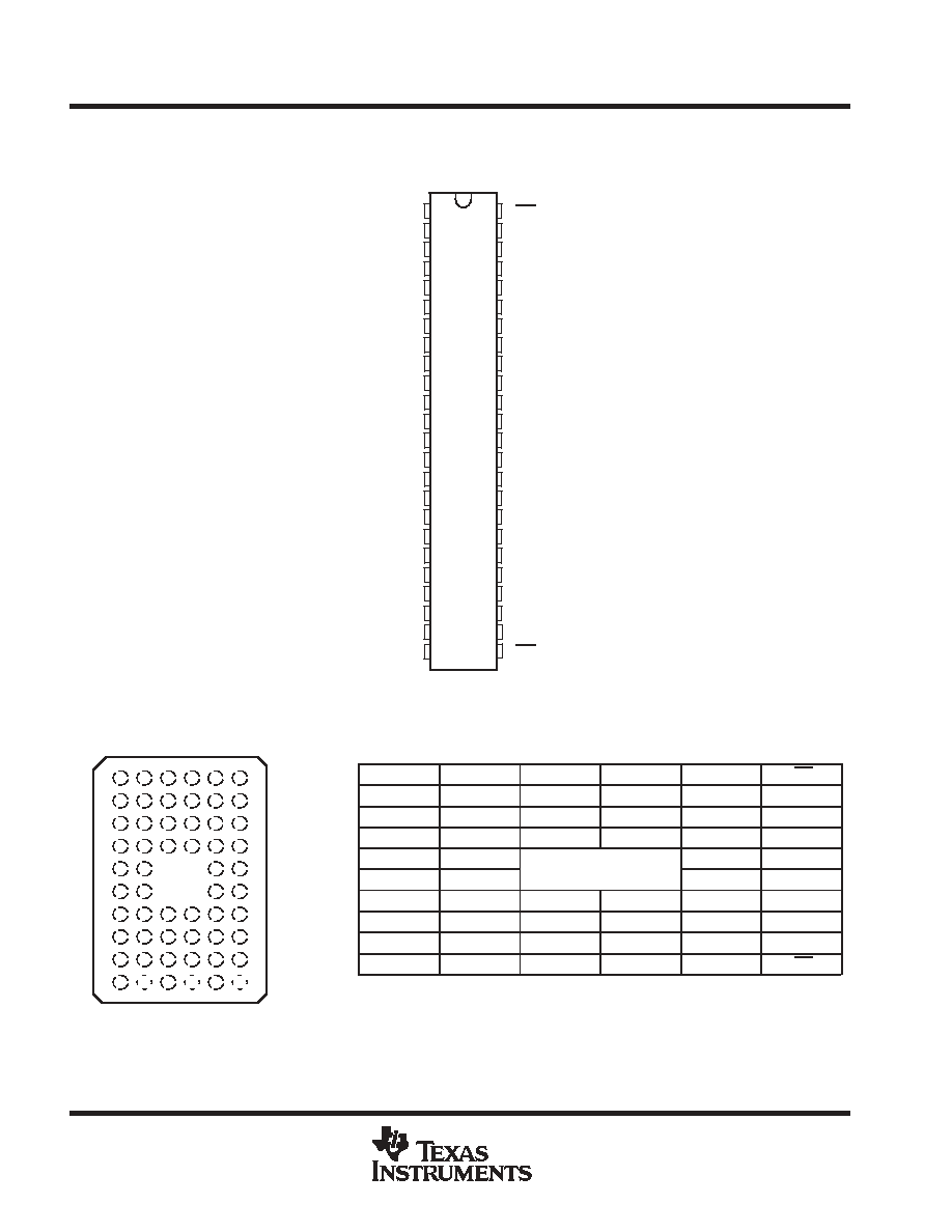
terminal assignments
DGG OR DGV PACKAGE
(TOP VIEW)
1
2
3
4
5
6
7
8
9
10
11
12
13
14
15
16
17
18
19
20
21
22
23
24
48
47
46
45
44
43
42
41
40
39
38
37
36
35
34
33
32
31
30
29
28
27
26
25
1DIR
1B1
1B2
GND
1B3
1B4
V
CCB
1B5
1B6
GND
1B7
1B8
2B1
2B2
GND
2B3
2B4
V
CCB
2B5
2B6
GND
2B7
2B8
2DIR
1OE
1A1
1A2
GND
1A3
1A4
V
CCA
1A5
1A6
GND
1A7
1A8
2A1
2A2
GND
2A3
2A4
V
CCA
2A5
2A6
GND
2A7
2A8
2OE
terminal assignments
1
2
3
4
5
6
A
1DIR
NC
NC
NC
NC
1OE
B
1B2
1B1
GND
GND
1A1
1A2
C
1B4
1B3
VCCB
VCCA
1A3
1A4
D
1B6
1B5
GND
GND
1A5
1A6
E
1B8
1B7
1A7
1A8
F
2B1
2B2
2A2
2A1
G
2B3
2B4
GND
GND
2A4
2A3
H
2B5
2B6
VCCB
VCCA
2A6
2A5
J
2B7
2B8
GND
GND
2A8
2A7
K
2DIR
NC
NC
NC
NC
2OE
NC - No internal connection
GQL PACKAGE
(TOP VIEW)
J
H
G
F
E
D
C
B
A
2
1
3
4
6
5
K

SN74AVCAH164245
16 BIT DUAL SUPPLY BUS TRANSCEIVER
WITH CONFIGURABLE VOLTAGE TRANSLATION AND 3 STATE OUTPUTS
SCES396A - JULY 2002 - REVISED MAY 2004
3
POST OFFICE BOX 655303
·
DALLAS, TEXAS 75265
FUNCTION TABLE
(each 8-bit section)
INPUTS
OPERATION
OE
DIR
OPERATION
L
L
B data to A bus
L
H
A data to B bus
H
X
Isolation
logic diagram (positive logic)
To Seven Other Channels
1DIR
1A1
1B1
1OE
To Seven Other Channels
2DIR
2A1
2B1
2OE
1
47
24
36
48
2
25
13
Pin numbers shown are for the DGG and DGV packages.

SN74AVCAH164245
16 BIT DUAL SUPPLY BUS TRANSCEIVER
WITH CONFIGURABLE VOLTAGE TRANSLATION AND 3 STATE OUTPUTS
SCES396A - JULY 2002 - REVISED MAY 2004
4
POST OFFICE BOX 655303
·
DALLAS, TEXAS 75265
absolute maximum ratings over operating free-air temperature range (unless otherwise noted)
Supply voltage range, V
CCA
and V
CCB
-0.5 V to 4.6 V
. . . . . . . . . . . . . . . . . . . . . . . . . . . . . . . . . . . . . . . . . . . . . .
Input voltage range, V
I
(see Note 1): I/O ports (A port)
-0.5 V to 4.6 V
. . . . . . . . . . . . . . . . . . . . . . . . . . . . . . . . .
I/O ports (B port)
-0.5 V to 4.6 V
. . . . . . . . . . . . . . . . . . . . . . . . . . . . . . . . .
Control inputs
-0.5 V to 4.6 V
. . . . . . . . . . . . . . . . . . . . . . . . . . . . . . . . . . .
Voltage range applied to any output in the high-impedance or power-off state, V
O
(see Note 1): (A port)
-0.5 V to 4.6 V
. . . . . . . . . . . . . . . . . . . . . . . . . . . . . . . . . . . . . . . . . . . . . . . . . . . . . . . . . . .
(B port)
-0.5 V to 4.6 V
. . . . . . . . . . . . . . . . . . . . . . . . . . . . . . . . . . . . . . . . . . . . . . . . . . . . . . . . . . .
Voltage range applied to any output in the high or low state, V
O
(see Notes 1 and 2): (A port)
-0.5 V to V
CCA
+ 0.5 V
. . . . . . . . . . . . . . . . . . . . . . . . . . . . . . . . . . . . . . . . . . . .
(B port)
-0.5 V to V
CCB
+ 0.5 V
. . . . . . . . . . . . . . . . . . . . . . . . . . . . . . . . . . . . . . . . . . . .
Input clamp current, I
IK
(V
I
< 0)
-50 mA
. . . . . . . . . . . . . . . . . . . . . . . . . . . . . . . . . . . . . . . . . . . . . . . . . . . . . . . . . . .
Output clamp current, I
OK
(V
O
< 0)
-50 mA
. . . . . . . . . . . . . . . . . . . . . . . . . . . . . . . . . . . . . . . . . . . . . . . . . . . . . . . .
Continuous output current, I
O
±
50 mA
. . . . . . . . . . . . . . . . . . . . . . . . . . . . . . . . . . . . . . . . . . . . . . . . . . . . . . . . . . . . .
Continuous current through V
CCA
, V
CCB
, or GND
±
100 mA
. . . . . . . . . . . . . . . . . . . . . . . . . . . . . . . . . . . . . . . . .
Package thermal impedance,
JA
(see Note 3): DGG package
70
°
C/W
. . . . . . . . . . . . . . . . . . . . . . . . . . . . . . .
DGV package
58
°
C/W
. . . . . . . . . . . . . . . . . . . . . . . . . . . . . . . .
GQL package
28
°
C/W
. . . . . . . . . . . . . . . . . . . . . . . . . . . . . . . .
Storage temperature range, T
stg
-65
°
C to 150
°
C
. . . . . . . . . . . . . . . . . . . . . . . . . . . . . . . . . . . . . . . . . . . . . . . . . . .
Stresses beyond those listed under "absolute maximum ratings" may cause permanent damage to the device. These are stress ratings only, and
functional operation of the device at these or any other conditions beyond those indicated under "recommended operating conditions" is not
implied. Exposure to absolute-maximum-rated conditions for extended periods may affect device reliability.
NOTES:
1. The input and output negative-voltage ratings may be exceeded if the input and output current ratings are observed.
2. The output positive-voltage rating may be exceeded up to 4.6 V maximum if the output current rating is observed.
3. The package thermal impedance is calculated in accordance with JESD 51-7.
SN74AVCAH164245
16 BIT DUAL SUPPLY BUS TRANSCEIVER
WITH CONFIGURABLE VOLTAGE TRANSLATION AND 3 STATE OUTPUTS
SCES396A - JULY 2002 - REVISED MAY 2004
5
POST OFFICE BOX 655303
·
DALLAS, TEXAS 75265
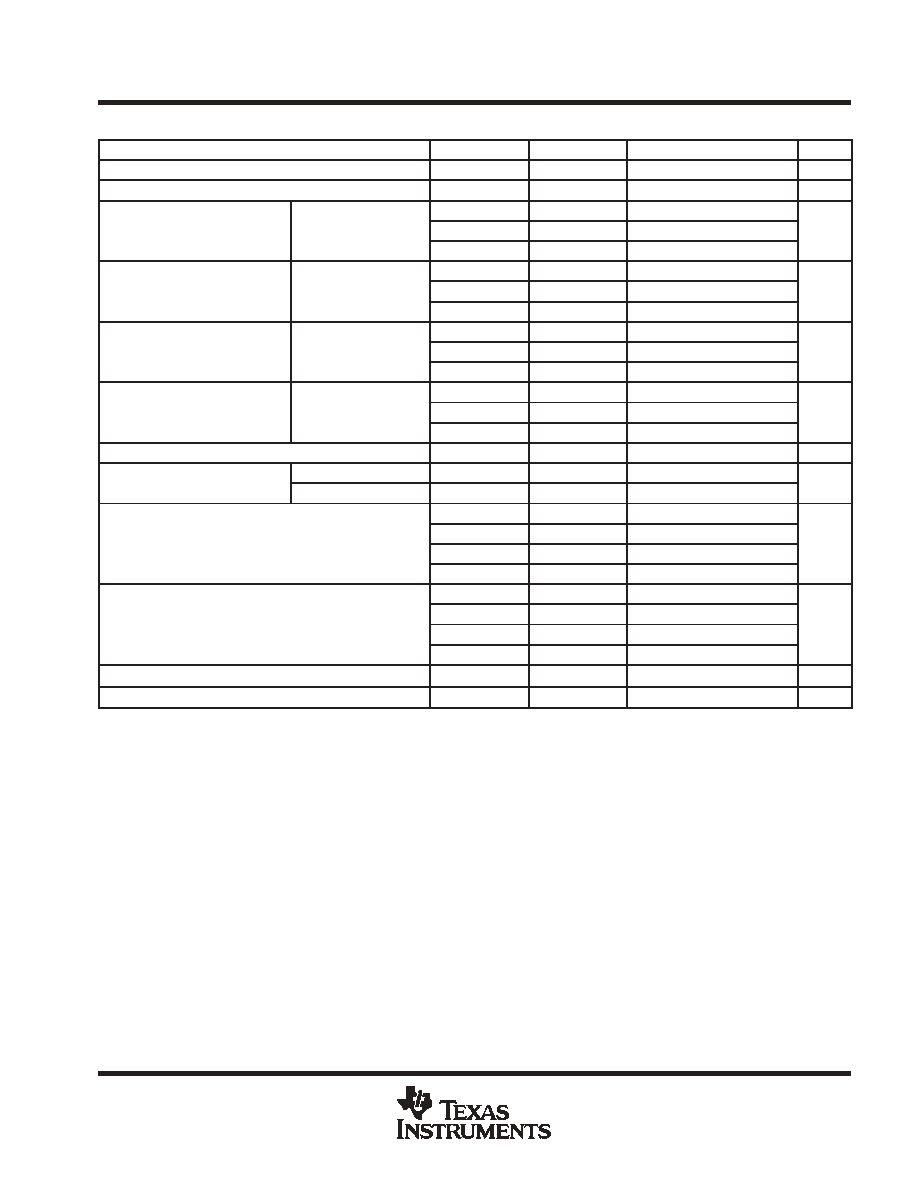
recommended operating conditions (see Notes 4 through 6)
VCCI
VCCO
MIN
MAX
UNIT
VCCA
Supply voltage
1.4
3.6
V
VCCB
Supply voltage
1.4
3.6
V
High-level input
1.4 V to 1.95 V
VCCI
×
0.65
VIH
High-level input
voltage
Data inputs
1.95 V to 2.7 V
1.7
V
VIH
voltage
Data inputs
2.7 V to 3.6 V
2
V
Low-level input
1.4 V to 1.95 V
VCCI
×
0.35
VIL
Low-level input
voltage
Data inputs
1.95 V to 2.7 V
0.7
V
VIL
voltage
Data inputs
2.7 V to 3.6 V
0.8
V
High-level input
Control inputs
1.4 V to 1.95 V
VCCA
×
0.65
VIH
High-level input
voltage
Control inputs
(Referenced to VCCA)
1.95 V to 2.7 V
1.7
V
VIH
voltage
(Referenced to VCCA)
2.7 V to 3.6 V
2
V
Low-level input
Control inputs
1.4 V to 1.95 V
VCCA
×
0.35
VIL
Low-level input
voltage
Control inputs
(Referenced to VCCA)
1.95 V to 2.7 V
0.7
V
VIL
voltage
(Referenced to VCCA)
2.7 V to 3.6 V
0.8
V
VI
Input voltage
0
3.6
V
VO
Output voltage
Active state
0
VCCO
V
VO
Output voltage
3-state
0
3.6
V
1.4 V to 1.6 V
-2
IOH
High-level output current
1.65 V to 1.95 V
-4
mA
IOH
High-level output current
2.3 V to 2.7 V
-8
mA
3 V to 3.6 V
-12
1.4 V to 1.6 V
2
IOL
Low-level output current
1.65 V to 1.95 V
4
mA
IOL
Low-level output current
2.3 V to 2.7 V
8
mA
3 V to 3.6 V
12
t/
v
Input transition rise or fall rate
5
ns/V
TA
Operating free-air temperature
-40
85
°
C
NOTES:
4. VCCI is the VCC associated with the data input port.
5. VCCO is the VCC associated with the output port.
6. All unused data inputs of the device must be held at VCCI or GND to ensure proper device operation. Refer to the TI application report,
Implications of Slow or Floating CMOS Inputs, literature number SCBA004.