
SN74ALVC244
OCTAL BUFFER/DRIVER
WITH 3 STATE OUTPUTS
SCES188D - FEBRUARY 1999 - REVISED SEPTEMBER 2003
1
POST OFFICE BOX 655303
·
DALLAS, TEXAS 75265
D
Operates From 1.65 V to 3.6 V
D
Max t
pd
of 2.8 ns at 3.3 V
D
±
24-mA Output Drive at 3.3 V
D
Latch-Up Performance Exceeds 250 mA Per
JESD 17
D
ESD Protection Exceeds JESD 22
- 2000-V Human-Body Model (A114-A)
- 200-V Machine Model (A115-A)
- 1000-V Charged-Device Model (C101)
1
2
3
4
5
6
7
8
9
10
20
19
18
17
16
15
14
13
12
11
1OE
1A1
2Y4
1A2
2Y3
1A3
2Y2
1A4
2Y1
GND
V
CC
2OE
1Y1
2A4
1Y2
2A3
1Y3
2A2
1Y4
2A1
DGV, DW, NS, OR PW PACKAGE
(TOP VIEW)
RGY PACKAGE
(TOP VIEW)
1
20
10
11
2
3
4
5
6
7
8
9
19
18
17
16
15
14
13
12
2OE
1Y1
2A4
1Y2
2A3
1Y3
2A2
1Y4
1A1
2Y4
1A2
2Y3
1A3
2Y2
1A4
2Y1
1OE
2A1
V
GND
CC
description/ordering information
This octal buffer/line driver is designed for 1.65-V to 3.6-V V
CC
operation.
The SN74ALVC244 is organized as two 4-bit line drivers with separate output-enable (OE) inputs. When OE
is low, the device passes data from the A inputs to the Y outputs. When OE is high, the outputs are in the
high-impedance state.
To ensure the high-impedance state during power up or power down, OE should be tied to V
CC
through a pullup
resistor; the minimum value of the resistor is determined by the current-sinking capability of the driver.
ORDERING INFORMATION
TA
PACKAGE
ORDERABLE
PART NUMBER
TOP-SIDE
MARKING
QFN - RGY
Tape and reel
SN74ALVC244RGYR
VA244
SOIC - DW
Tube
SN74ALVC244DW
ALVC244
SOIC - DW
Tape and reel
SN74ALVC244DWR
ALVC244
-40
°
C to 85
°
C
SOP - NS
Tape and reel
SN74ALVC244NSR
ALVC244
-40 C to 85 C
TSSOP - PW
Tube
SN74ALVC244PW
VA244
TSSOP - PW
Tape and reel
SN74ALVC244PWR
VA244
TVSOP - DGV
Tape and reel
SN74ALVC244DGVR
VA244
Package drawings, standard packing quantities, thermal data, symbolization, and PCB design
guidelines are available at www.ti.com/sc/package.
Copyright
2003, Texas Instruments Incorporated
Please be aware that an important notice concerning availability, standard warranty, and use in critical applications of
Texas Instruments semiconductor products and disclaimers thereto appears at the end of this data sheet.
PRODUCTION DATA information is current as of publication date.
Products conform to specifications per the terms of Texas Instruments
standard warranty. Production processing does not necessarily include
testing of all parameters.

SN74ALVC244
OCTAL BUFFER/DRIVER
WITH 3 STATE OUTPUTS
SCES188D - FEBRUARY 1999 - REVISED SEPTEMBER 2003
2
POST OFFICE BOX 655303
·
DALLAS, TEXAS 75265
FUNCTION TABLE
(each buffer)
INPUTS
OUTPUT
OE
A
OUTPUT
Y
L
H
H
L
L
L
H
X
Z
logic diagram (positive logic)
1
2
18
1Y1
1OE
1A1
4
16
1Y2
1A2
6
14
1Y3
1A3
8
12
1Y4
1A4
19
11
9
2Y1
2OE
2A1
13
7
2Y2
2A2
15
5
2Y3
2A3
17
3
2Y4
2A4
absolute maximum ratings over operating free-air temperature range (unless otherwise noted)
Supply voltage range, V
CC
-0.5 V to 4.6 V
. . . . . . . . . . . . . . . . . . . . . . . . . . . . . . . . . . . . . . . . . . . . . . . . . . . . . . . . .
Input voltage range, V
I
(see Note 1)
-0.5 V to 4.6 V
. . . . . . . . . . . . . . . . . . . . . . . . . . . . . . . . . . . . . . . . . . . . . . . . .
Output voltage range, V
O
(see Notes 1 and 2)
-0.5 V to V
CC
+ 0.5 V
. . . . . . . . . . . . . . . . . . . . . . . . . . . . . . . . . .
Input clamp current, I
IK
(V
I
< 0)
-50 mA
. . . . . . . . . . . . . . . . . . . . . . . . . . . . . . . . . . . . . . . . . . . . . . . . . . . . . . . . . . .
Output clamp current, I
OK
(V
O
< 0)
-50 mA
. . . . . . . . . . . . . . . . . . . . . . . . . . . . . . . . . . . . . . . . . . . . . . . . . . . . . . . .
Continuous output current, I
O
±
50 mA
. . . . . . . . . . . . . . . . . . . . . . . . . . . . . . . . . . . . . . . . . . . . . . . . . . . . . . . . . . . . .
Continuous current through V
CC
or GND
±
100 mA
. . . . . . . . . . . . . . . . . . . . . . . . . . . . . . . . . . . . . . . . . . . . . . . . . .
Package thermal impedance,
JA
(see Note 3): DGV package
92
°
C/W
. . . . . . . . . . . . . . . . . . . . . . . . . . . . . . . .
(see Note 3): DW package
58
°
C/W
. . . . . . . . . . . . . . . . . . . . . . . . . . . . . . . . .
(see Note 3): NS package
60
°
C/W
. . . . . . . . . . . . . . . . . . . . . . . . . . . . . . . . .
(see Note 3): PW package
83
°
C/W
. . . . . . . . . . . . . . . . . . . . . . . . . . . . . . . . .
(see Note 4): RGY package
37
°
C/W
. . . . . . . . . . . . . . . . . . . . . . . . . . . . . . . .
Storage temperature range, T
stg
-65
°
C to 150
°
C
. . . . . . . . . . . . . . . . . . . . . . . . . . . . . . . . . . . . . . . . . . . . . . . . . . .
Stresses beyond those listed under "absolute maximum ratings" may cause permanent damage to the device. These are stress ratings only, and
functional operation of the device at these or any other conditions beyond those indicated under "recommended operating conditions" is not
implied. Exposure to absolute-maximum-rated conditions for extended periods may affect device reliability.
NOTES:
1. The input negative-voltage and output voltage ratings may be exceeded if the input and output current ratings are observed.
2. This value is limited to 4.6 V maximum.
3. The package thermal impedance is calculated in accordance with JESD 51-7.
4. The package thermal impedance is calculated in accordance with JESD 51-5.

SN74ALVC244
OCTAL BUFFER/DRIVER
WITH 3 STATE OUTPUTS
SCES188D - FEBRUARY 1999 - REVISED SEPTEMBER 2003
3
POST OFFICE BOX 655303
·
DALLAS, TEXAS 75265
recommended operating conditions (see Note 5)
MIN
MAX
UNIT
VCC
Supply voltage
1.65
3.6
V
VCC = 1.65 V to 1.95 V
0.65
×
VCC
VIH
High-level input voltage
VCC = 2.3 V to 2.7 V
1.7
V
VIH
High-level input voltage
VCC = 2.7 V to 3.6 V
2
V
VCC = 1.65 V to 1.95 V
0.35
×
VCC
VIL
Low-level input voltage
VCC = 2.3 V to 2.7 V
0.7
V
VIL
Low-level input voltage
VCC = 2.7 V to 3.6 V
0.8
V
VI
Input voltage
0
3.6
V
VO
Output voltage
0
VCC
V
VCC = 1.65 V
-4
IOH
High-level output current
VCC = 2.3 V
-12
mA
IOH
High-level output current
VCC = 2.7 V
-12
mA
VCC = 3 V
-24
VCC = 1.65 V
4
IOL
Low-level output current
VCC = 2.3 V
12
mA
IOL
Low-level output current
VCC = 2.7 V
12
mA
VCC = 3 V
24
t/
v
Input transition rise or fall rate
5
ns/V
TA
Operating free-air temperature
-40
85
°
C
NOTE 5: All unused inputs of the device must be held at VCC or GND to ensure proper device operation. Refer to the TI application report,
Implications of Slow or Floating CMOS Inputs, literature number SCBA004.

SN74ALVC244
OCTAL BUFFER/DRIVER
WITH 3 STATE OUTPUTS
SCES188D - FEBRUARY 1999 - REVISED SEPTEMBER 2003
4
POST OFFICE BOX 655303
·
DALLAS, TEXAS 75265
electrical characteristics over recommended operating free-air temperature range (unless
otherwise noted)
PARAMETER
TEST CONDITIONS
VCC
MIN
TYP
MAX
UNIT
IOH = -100
µ
A
1.65 V to 3.6 V
VCC-0.2
IOH = -4 mA
1.65 V
1.2
IOH = -6 mA
2.3 V
2
VOH
2.3 V
1.7
V
VOH
IOH = -12 mA
2.7 V
2.2
V
IOH = -12 mA
3 V
2.4
IOH = -24 mA
3 V
2
IOL = 100
µ
A
1.65 V to 3.6 V
0.2
IOL = 4 mA
1.65 V
0.45
VOL
IOL = 6 mA
2.3 V
0.4
V
VOL
IOL = 12 mA
2.3 V
0.7
V
IOL = 12 mA
2.7 V
0.4
IOL = 24 mA
3 V
0.55
II
VI = VCC or GND
3.6 V
±
5
µ
A
IOZ
VO = VCC or GND
3.6 V
±
10
µ
A
ICC
VI = VCC or GND,
IO = 0
3.6 V
10
µ
A
ICC
One input at VCC - 0.6 V,
Other inputs at VCC or GND
3 V to 3.6 V
750
µ
A
Ci
Control inputs
VI = VCC or GND
3.3 V
4.5
pF
Ci
Data inputs
VI = VCC or GND
3.3 V
4.5
pF
Co
Outputs
VO = VCC or GND
3.3 V
7.5
pF
All typical values are at VCC = 3.3 V, TA = 25
°
C.
switching characteristics over recommended operating free-air temperature range (unless
otherwise noted) (see Figure 1)
PARAMETER
FROM
(INPUT)
TO
(OUTPUT)
VCC = 1.8 V
±
0.15 V
VCC = 2.5 V
±
0.2 V
VCC = 2.7 V
VCC = 3.3 V
±
0.3 V
UNIT
PARAMETER
(INPUT)
(OUTPUT)
MIN
MAX
MIN
MAX
MIN
MAX
MIN
MAX
UNIT
tpd
A
Y
1
4.4
1
3.1
3.1
1.1
2.8
ns
ten
OE
Y
1.8
6.9
1.5
5.4
5.3
1.5
4.5
ns
tdis
OE
Y
1.8
5.9
1
4.1
4.4
1.7
4.2
ns
operating characteristics, T
A
= 25
°
C
PARAMETER
TEST CONDITIONS
VCC = 1.8 V VCC = 2.5 V VCC = 3.3 V
UNIT
PARAMETER
TEST CONDITIONS
TYP
TYP
TYP
UNIT
Cpd
Power dissipation capacitance
Outputs enabled
CL = 0,
f = 10 MHz
22
23
26
pF
Cpd
Power dissipation capacitance
per buffer/driver
Outputs disabled
CL = 0,
f = 10 MHz
1
1
1
pF
SN74ALVC244
OCTAL BUFFER/DRIVER
WITH 3 STATE OUTPUTS
SCES188D - FEBRUARY 1999 - REVISED SEPTEMBER 2003
5
POST OFFICE BOX 655303
·
DALLAS, TEXAS 75265
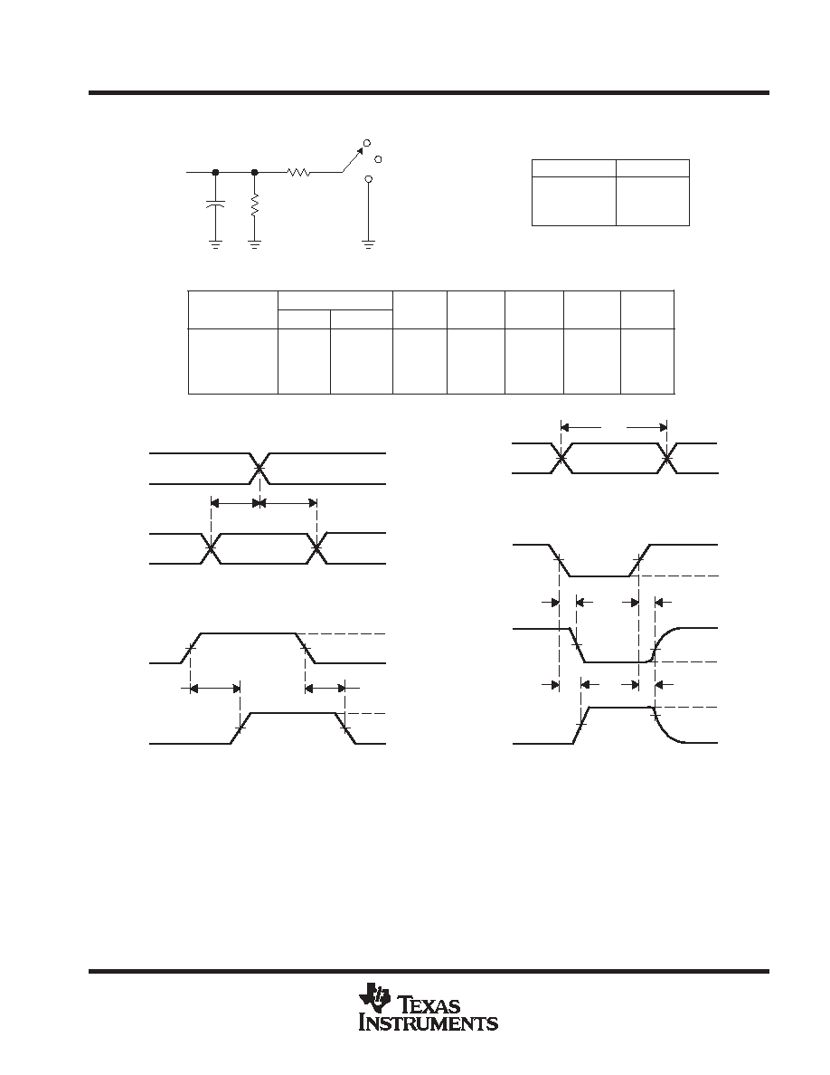
PARAMETER MEASUREMENT INFORMATION
VM
VM
VM
VM
VM
VM
VM
VM
VOH
VOL
th
tsu
From Output
Under Test
CL
(see Note A)
LOAD CIRCUIT
S1
Open
GND
RL
RL
Output
Control
(low-level
enabling)
Output
Waveform 1
S1 at VLOAD
(see Note B)
Output
Waveform 2
S1 at GND
(see Note B)
tPZL
tPZH
tPLZ
tPHZ
0 V
VOL + V
VOH - V
0 V
VI
0 V
0 V
tw
VI
VI
VOLTAGE WAVEFORMS
SETUP AND HOLD TIMES
VOLTAGE WAVEFORMS
PULSE DURATION
VOLTAGE WAVEFORMS
ENABLE AND DISABLE TIMES
Timing
Input
Data
Input
Input
tpd
tPLZ/tPZL
tPHZ/tPZH
Open
VLOAD
GND
TEST
S1
NOTES: A. CL includes probe and jig capacitance.
B. Waveform 1 is for an output with internal conditions such that the output is low except when disabled by the output control.
Waveform 2 is for an output with internal conditions such that the output is high except when disabled by the output control.
C. All input pulses are supplied by generators having the following characteristics: PRR
10 MHz, ZO = 50
.
D. The outputs are measured one at a time with one transition per measurement.
E. tPLZ and tPHZ are the same as tdis.
F. tPZL and tPZH are the same as ten.
G. tPLH and tPHL are the same as tpd.
H. All parameters and waveforms are not applicable to all devices.
0 V
VI
VM
tPHL
VM
VM
VI
0 V
VOH
VOL
Input
Output
VOLTAGE WAVEFORMS
PROPAGATION DELAY TIMES
VM
VM
tPLH
VLOAD
VLOAD/2
1.8 V
±
0.15 V
2.5
±
0.2 V
2.7 V
3.3 V
±
0.3 V
1 k
500
500
500
VCC
RL
2
×
VCC
2
×
VCC
6 V
6 V
VLOAD
CL
30 pF
30 pF
50 pF
50 pF
0.15 V
0.15 V
0.3 V
0.3 V
V
VCC
VCC
2.7 V
2.7 V
VI
VCC/2
VCC/2
1.5 V
1.5 V
VM
tr/tf
2 ns
2 ns
2.5 ns
2.5 ns
INPUT
Figure 1. Load Circuit and Voltage Waveforms