SN74ALS641A, SN74ALS642A, SN74AS641
OCTAL BUS TRANSCEIVERS
WITH OPEN-COLLECTOR OUTPUTS
SDAS300 MARCH 1995
Copyright
©
1995, Texas Instruments Incorporated
1
POST OFFICE BOX 655303
·
DALLAS, TEXAS 75265
·
Bidirectional Bus Transceivers in
High-Density 20-Pin Packages
·
Choice of True or Inverting Logic
·
Package Options Include Plastic
Small-Outline (DW) Packages and
Standard Plastic (N) 300-mil DIPs
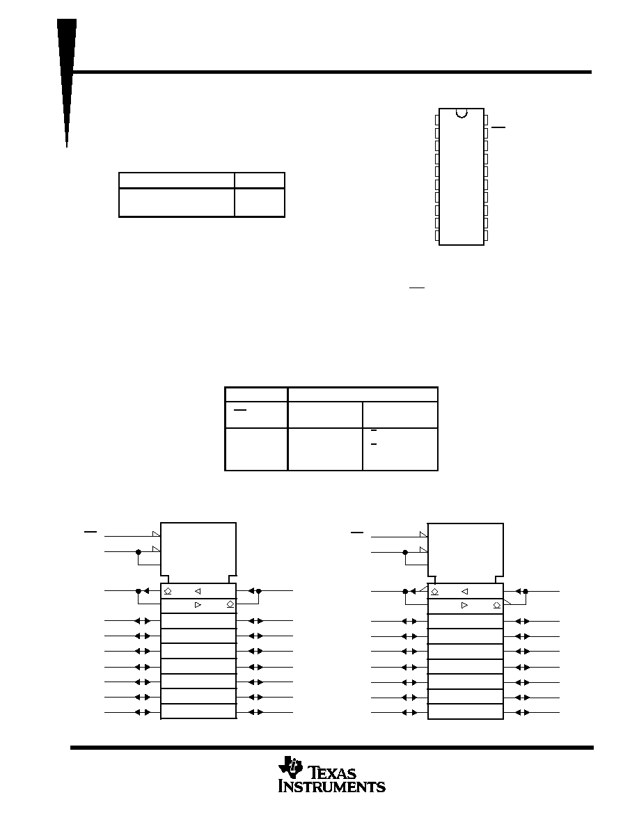
DEVICE
LOGIC
SN74ALS641A, SN74AS641
True
SN74ALS642A
Inverting
description
These octal bus transceivers are designed for
asynchronous two-way communication between
data buses. These devices transmit data from the A bus to the B bus or from the B bus to the A bus, depending
upon the level at the direction-control (DIR) input. The output-enable (OE) input disables the device so that the
buses are effectively isolated.
The -1 versions of the SN74ALS641A and SN74ALS642A are identical to the standard versions, except that
the recommended maximum I
OL
is increased to 48 mA in the -1 versions.
The SN74ALS641A, SN74ALS642A, and SN74AS641 are characterized for operation from 0
°
C to 70
°
C.
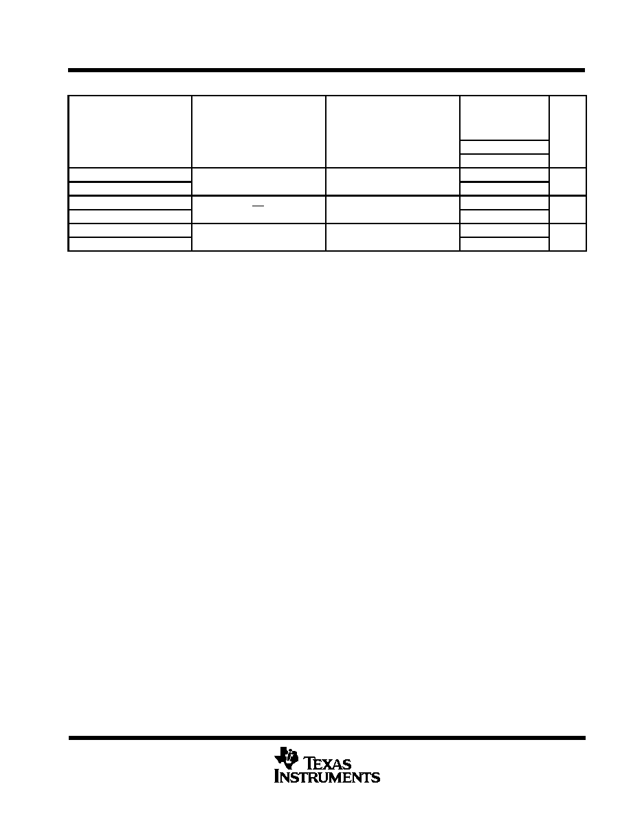
FUNCTION TABLE
INPUTS
OPERATION
OE
DIR
SN74ALS641A
SN74AS641
SN74ALS642A
L
L
B data to A bus
B data to A bus
L
H
A data to B bus
A data to B bus
H
X
Isolation
Isolation
logic symbols
B2
17
B3
16
B4
15
A5
6
A6
7
A7
8
A8
9
A2
3
A3
4
A4
5
OE
A1
2
G3
19
3 EN2 [AB]
B5
14
B6
13
B7
12
B8
11
B1
18
3 EN1 [BA]
1
DIR
1
2
SN74ALS641A, SN74AS641
B2
17
B3
16
B4
15
A5
6
A6
7
A7
8
A8
9
A2
3
A3
4
A4
5
OE
A1
2
G3
19
3 EN2 [AB]
B5
14
B6
13
B7
12
B8
11
B1
18
3 EN1 [BA]
1
DIR
1
2
SN74ALS642A
These symbols are in accordance with ANSI/IEEE Std 91-1984 and IEC Publication 617-12.
1
2
3
4
5
6
7
8
9
10
20
19
18
17
16
15
14
13
12
11
DIR
A1
A2
A3
A4
A5
A6
A7
A8
GND
V
CC
OE
B1
B2
B3
B4
B5
B6
B7
B8
DW OR N PACKAGE
(TOP VIEW)
PRODUCTION DATA information is current as of publication date.
Products conform to specifications per the terms of Texas Instruments
standard warranty. Production processing does not necessarily include
testing of all parameters.
SN74ALS641A, SN74ALS642A, SN74AS641
OCTAL BUS TRANSCEIVERS
WITH OPEN-COLLECTOR OUTPUTS
SDAS300 MARCH 1995
2
POST OFFICE BOX 655303
·
DALLAS, TEXAS 75265
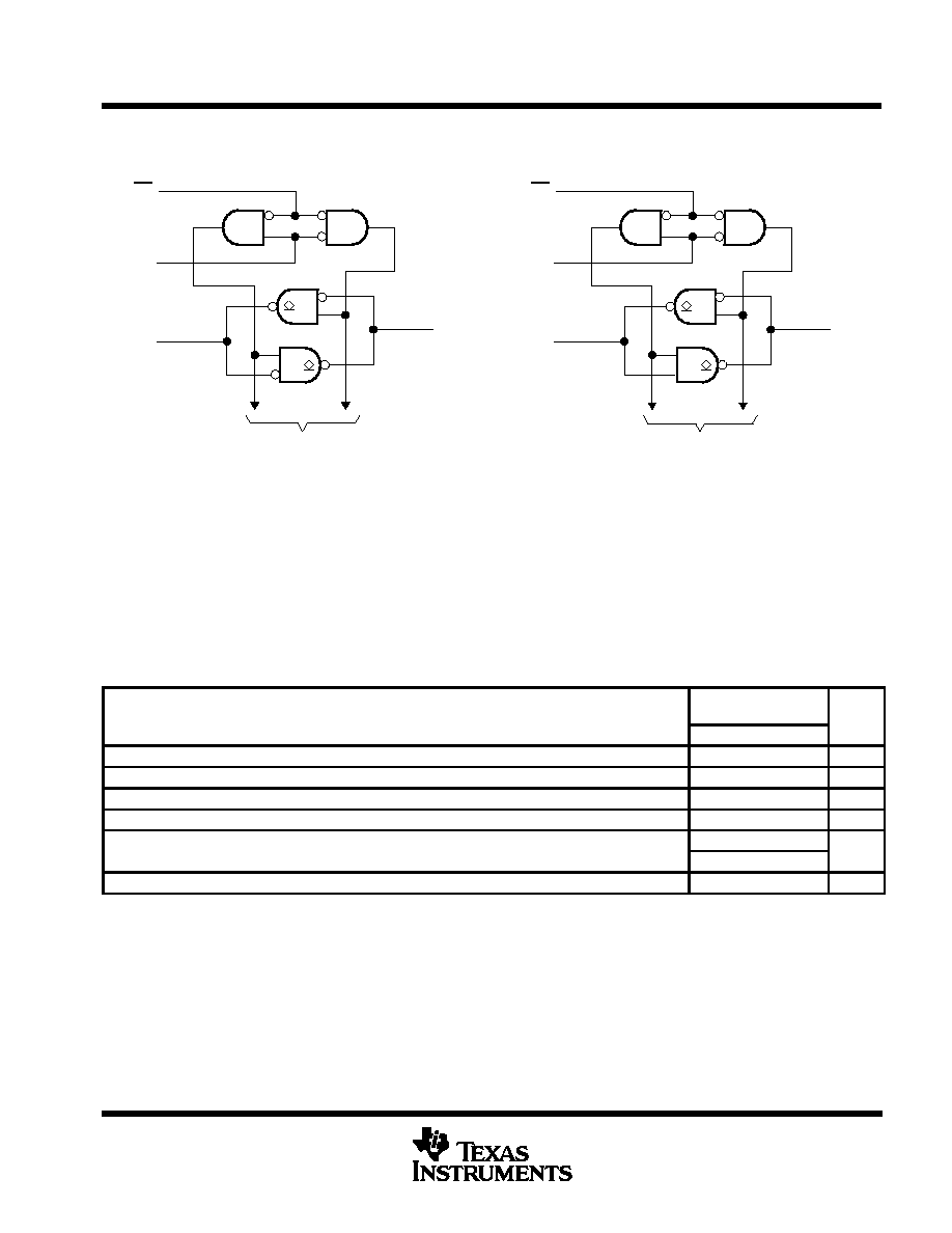
logic diagrams (positive logic)
SN74ALS641A, SN74AS641
A1
B1
19
1
18
2
OE
DIR
To Seven Other Transceivers
SN74ALS642A
A1
B1
19
1
18
2
OE
DIR
To Seven Other Transceivers
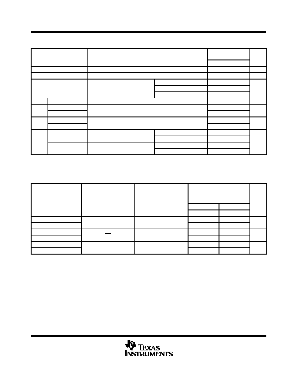
absolute maximum ratings over operating free-air temperature range (unless otherwise noted)
Supply voltage, V
CC
7 V
. . . . . . . . . . . . . . . . . . . . . . . . . . . . . . . . . . . . . . . . . . . . . . . . . . . . . . . . . . . . . . . . . . . . . . . .
Input voltage, V
I
: All inputs and I/O ports
7 V
. . . . . . . . . . . . . . . . . . . . . . . . . . . . . . . . . . . . . . . . . . . . . . . . . . . . . .
Operating free-air temperature range, T
A
: SN74ALS641A, SN74ALS642A
0
°
C to 70
°
C
. . . . . . . . . . . . . . . . .
Storage temperature range
65
°
C to 150
°
C
. . . . . . . . . . . . . . . . . . . . . . . . . . . . . . . . . . . . . . . . . . . . . . . . . . . . . . .
Stresses beyond those listed under "absolute maximum ratings" may cause permanent damage to the device. These are stress ratings only, and
functional operation of the device at these or any other conditions beyond those indicated under "recommended operating conditions" is not
implied. Exposure to absolute-maximum-rated conditions for extended periods may affect device reliability.
recommended operating conditions
SN74ALS641A
SN74ALS642A
UNIT
MIN
NOM
MAX
VCC
Supply voltage
4.5
5
5.5
V
VIH
High-level input voltage
2
V
VIL
Low-level input voltage
0.8
V
VOH
High-level output voltage
5.5
V
IOL
Low level output current
24
mA
IOL
Low-level output current
48
mA
TA
Operating free-air temperature
0
70
°
C
Applies only to the -1 version and only if VCC is between 4.75 V and 5.25 V
SN74ALS641A, SN74ALS642A, SN74AS641
OCTAL BUS TRANSCEIVERS
WITH OPEN-COLLECTOR OUTPUTS
SDAS300 MARCH 1995
3
POST OFFICE BOX 655303
·
DALLAS, TEXAS 75265
electrical characteristics over recommended operating free-air temperature range (unless
otherwise noted)
PARAMETER
TEST CONDITIONS
SN74ALS641A
SN74ALS642A
UNIT
MIN
TYP
MAX
VIK
VCC = 4.5 V,
II = 18 mA
1.5
V
IOH
VCC = 4.5 V,
VOH = 5.5 V
0.1
mA
IOL = 12 mA
0.25
0.4
VOL
VCC = 4.5 V
IOL = 24 mA
0.35
0.5
V
IOL = 48 mA
0.35
0.5
II
Control inputs
VCC = 5.5 V,
VI = 7 V
0.1
mA
IIH
Control inputs
VCC = 5 5 V
VI = 2 7 V
20
µ
A
IIH
A or B ports§
VCC = 5.5 V,
VI = 2.7 V
20
µ
A
IIL
Control inputs
VCC = 5 5 V
VI = 0 4 V
0.1
mA
IIL
A or B ports§
VCC = 5.5 V,
VI = 0.4 V
0.1
mA
SN74ALS641A
VCC = 5 5 V
Outputs high
25
37
ICC
SN74ALS641A
VCC = 5.5 V
Outputs low
33
47
mA
ICC
SN74ALS642A
VCC = 5 5 V
Outputs high
8
15
mA
SN74ALS642A
VCC = 5.5 V
Outputs low
18
28
All typical values are at VCC = 5 V, TA = 25
°
C.
Applies only to the -1 version and only if VCC is between 4.75 V and 5.25 V
§ For I/O ports, the parameters IIH and IIL include the off-state output current.
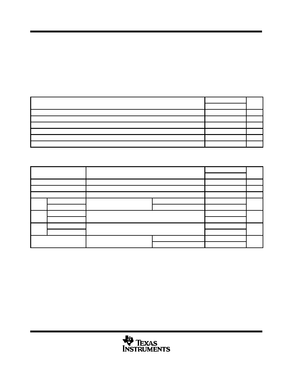
switching characteristics (see Figure 1)
PARAMETER
FROM
(INPUT)
TO
(OUTPUT)
VCC = 4.5 V to 5.5 V,
CL = 50 pF,
RL = 680
,
TA = MIN to MAX¶
UNIT
(INPUT)
(OUTPUT)
SN74ALS641A
SN74ALS642A
MIN
MAX
MIN
MAX
tPLH
A or B
B or A
5
25
10
30
ns
tPHL
A or B
B or A
3
18
5
22
ns
tPLH
OE
A or B
8
30
10
30
ns
tPHL
OE
A or B
8
30
15
38
ns
tPLH
DIR
A or B
8
32
10
30
ns
tPHL
DIR
A or B
8
32
15
38
ns
¶ For conditions shown as MIN or MAX, use the appropriate value specified under recommended operating conditions.
SN74ALS641A, SN74ALS642A, SN74AS641
OCTAL BUS TRANSCEIVERS
WITH OPEN-COLLECTOR OUTPUTS
SDAS300 MARCH 1995
4
POST OFFICE BOX 655303
·
DALLAS, TEXAS 75265
absolute maximum ratings over operating free-air temperature range (unless otherwise noted)
Supply voltage, V
CC
7 V
. . . . . . . . . . . . . . . . . . . . . . . . . . . . . . . . . . . . . . . . . . . . . . . . . . . . . . . . . . . . . . . . . . . . . . . .
Input voltage, V
I
: All inputs and I/O ports
7 V
. . . . . . . . . . . . . . . . . . . . . . . . . . . . . . . . . . . . . . . . . . . . . . . . . . . . . .
Operating free-air temperature range, T
A
: SN74AS641
0
°
C to 70
°
C
. . . . . . . . . . . . . . . . . . . . . . . . . . . . . . . . . .
Storage temperature range
65
°
C to 150
°
C
. . . . . . . . . . . . . . . . . . . . . . . . . . . . . . . . . . . . . . . . . . . . . . . . . . . . . . .
Stresses beyond those listed under "absolute maximum ratings" may cause permanent damage to the device. These are stress ratings only, and
functional operation of the device at these or any other conditions beyond those indicated under "recommended operating conditions" is not
implied. Exposure to absolute-maximum-rated conditions for extended periods may affect device reliability.
recommended operating conditions
SN74AS641
UNIT
MIN
NOM
MAX
UNIT
VCC
Supply voltage
4.5
5
5.5
V
VIH
High-level input voltage
2
V
VIL
Low-level input voltage
0.8
V
VOH
High-level output voltage
5.5
V
IOL
Low-level output current
64
mA
TA
Operating free-air temperature
0
70
°
C
electrical characteristics over recommended operating free-air temperature range (unless
otherwise noted)
PARAMETER
TEST CONDITIONS
SN74AS641
UNIT
PARAMETER
TEST CONDITIONS
MIN
TYP
MAX
UNIT
VIK
VCC = 4.5 V,
II = 18 mA
1.2
V
IOH
VCC = 4.5 V,
VOH = 5.5 V
0.1
mA
VOL
VCC = 4.5 V,
IOL = 64 mA
0.35
0.55
V
II
Control inputs
VCC = 5 5 V
VI = 7 V
0.1
mA
II
A or B ports
VCC = 5.5 V
VI = 5.5 V
0.1
mA
IIH
Control inputs
VCC = 5 5 V
VI = 2 7 V
20
µ
A
IIH
A or B ports§
VCC = 5.5 V,
VI = 2.7 V
70
µ
A
IIL
Control inputs
VCC = 5 5 V
VI = 0 4 V
0.5
mA
IIL
A or B ports§
VCC = 5.5 V,
VI = 0.4 V
0.75
mA
ICC
VCC = 5 5 V
Outputs high
50
82
mA
ICC
VCC = 5.5 V
Outputs low
84
136
mA
All typical values are at VCC = 5 V, TA = 25
°
C.
§ For I/O ports, the parameters IIH and IIL include the off-state output current.
SN74ALS641A, SN74ALS642A, SN74AS641
OCTAL BUS TRANSCEIVERS
WITH OPEN-COLLECTOR OUTPUTS
SDAS300 MARCH 1995
5
POST OFFICE BOX 655303
·
DALLAS, TEXAS 75265
switching characteristics (see Figure 1)
PARAMETER
FROM
(INPUT)
TO
(OUTPUT)
VCC = 4.5 V to 5.5 V,
CL = 50 pF,
RL = 680
,
TA = MIN to MAX
UNIT
(INPUT)
(OUTPUT)
SN74AS641
MIN
MAX
tPLH
A or B
B or A
5
21
ns
tPHL
A or B
B or A
1
7.5
ns
tPLH
OE
A or B
5
21
ns
tPHL
OE
A or B
1
9
ns
tPLH
DIR
A or B
5
22
ns
tPHL
DIR
A or B
1
10
ns
For conditions shown as MIN or MAX, use the appropriate value specified under recommended operating conditions.
SN74ALS641A, SN74ALS642A, SN74AS641
OCTAL BUS TRANSCEIVERS
WITH OPEN-COLLECTOR OUTPUTS
SDAS300 MARCH 1995
6
POST OFFICE BOX 655303
·
DALLAS, TEXAS 75265
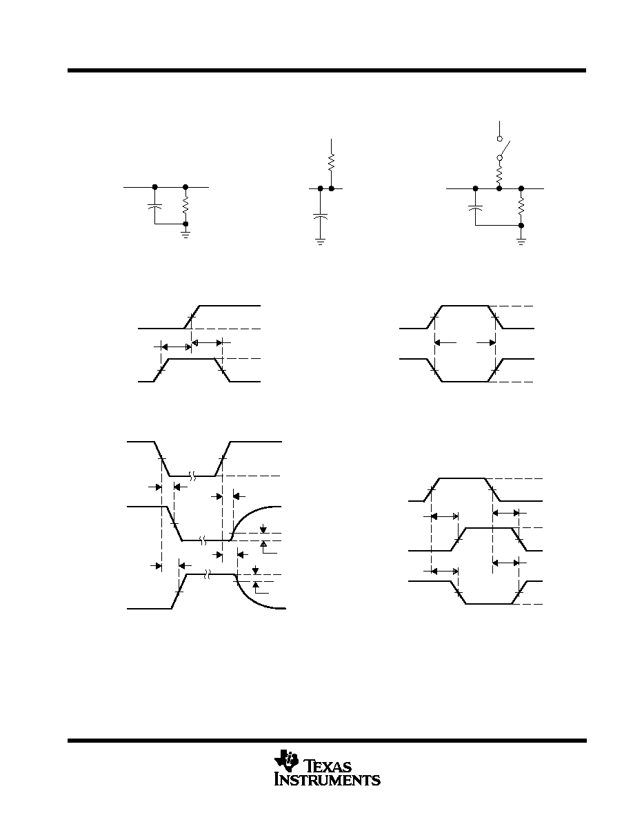
PARAMETER MEASUREMENT INFORMATION
SERIES 54ALS/ 74ALS AND 54AS/ 74AS DEVICES
tPHZ
tPLZ
tPHL
tPLH
0.3 V
tPZL
tPZH
tPLH
tPHL
LOAD CIRCUIT
FOR 3-STATE OUTPUTS
From Output
Under Test
Test
Point
R1
S1
CL
(see Note A)
7 V
1.3 V
1.3 V
1.3 V
3.5 V
3.5 V
0.3 V
0.3 V
th
tsu
VOLTAGE WAVEFORMS
SETUP AND HOLD TIMES
Timing
Input
Data
Input
1.3 V
1.3 V
3.5 V
3.5 V
0.3 V
0.3 V
High-Level
Pulse
Low-Level
Pulse
tw
VOLTAGE WAVEFORMS
PULSE DURATIONS
Input
Out-of-Phase
Output
(see Note C)
1.3 V
1.3 V
1.3 V
1.3 V
1.3 V
1.3 V
1.3 V
1.3 V
1.3 V
1.3 V
3.5 V
3.5 V
0.3 V
0.3 V
VOL
VOH
VOH
VOL
Output
Control
(low-level
enabling)
Waveform 1
S1 Closed
(see Note B)
Waveform 2
S1 Open
(see Note B)
[
0 V
VOH
VOL
[
3.5 V
In-Phase
Output
0.3 V
1.3 V
1.3 V
VOLTAGE WAVEFORMS
PROPAGATION DELAY TIMES
VOLTAGE WAVEFORMS
ENABLE AND DISABLE TIMES, 3-STATE OUTPUTS
R2
VCC
RL
Test
Point
From Output
Under Test
CL
(see Note A)
LOAD CIRCUIT
FOR OPEN-COLLECTOR OUTPUTS
LOAD CIRCUIT FOR
BI-STATE
TOTEM-POLE OUTPUTS
From Output
Under Test
Test
Point
CL
(see Note A)
RL
RL = R1 = R2
NOTES: A. CL includes probe and jig capacitance.
B. Waveform 1 is for an output with internal conditions such that the output is low except when disabled by the output control.
Waveform 2 is for an output with internal conditions such that the output is high except when disabled by the output control.
C. When measuring propagation delay items of 3-state outputs, switch S1 is open.
D. All input pulses have the following characteristics: PRR
1 MHz, tr = tf = 2 ns, duty cycle = 50%.
E. The outputs are measured one at a time with one transition per measurement.
Figure 1. Load Circuits and Voltage Waveforms

IMPORTANT NOTICE
Texas Instruments and its subsidiaries (TI) reserve the right to make changes to their products or to discontinue
any product or service without notice, and advise customers to obtain the latest version of relevant information
to verify, before placing orders, that information being relied on is current and complete. All products are sold
subject to the terms and conditions of sale supplied at the time of order acknowledgement, including those
pertaining to warranty, patent infringement, and limitation of liability.
TI warrants performance of its semiconductor products to the specifications applicable at the time of sale in
accordance with TI's standard warranty. Testing and other quality control techniques are utilized to the extent
TI deems necessary to support this warranty. Specific testing of all parameters of each device is not necessarily
performed, except those mandated by government requirements.
CERTAIN APPLICATIONS USING SEMICONDUCTOR PRODUCTS MAY INVOLVE POTENTIAL RISKS OF
DEATH, PERSONAL INJURY, OR SEVERE PROPERTY OR ENVIRONMENTAL DAMAGE ("CRITICAL
APPLICATIONS"). TI SEMICONDUCTOR PRODUCTS ARE NOT DESIGNED, AUTHORIZED, OR
WARRANTED TO BE SUITABLE FOR USE IN LIFE-SUPPORT DEVICES OR SYSTEMS OR OTHER
CRITICAL APPLICATIONS. INCLUSION OF TI PRODUCTS IN SUCH APPLICATIONS IS UNDERSTOOD TO
BE FULLY AT THE CUSTOMER'S RISK.
In order to minimize risks associated with the customer's applications, adequate design and operating
safeguards must be provided by the customer to minimize inherent or procedural hazards.
TI assumes no liability for applications assistance or customer product design. TI does not warrant or represent
that any license, either express or implied, is granted under any patent right, copyright, mask work right, or other
intellectual property right of TI covering or relating to any combination, machine, or process in which such
semiconductor products or services might be or are used. TI's publication of information regarding any third
party's products or services does not constitute TI's approval, warranty or endorsement thereof.
Copyright
©
1998, Texas Instruments Incorporated