SN54ALS136, SN54AS136, SN74ALS136, SN74AS136
QUADRUPLE 2-INPUT EXCLUSIVE-OR GATES
WITH OPEN-COLLECTOR OUTPUTS
SDAS162 MARCH 1984REVISED OCTOBER 1988
POST OFFICE BOX 655303
·
DALLAS, TEXAS 75265
Copyright
©
1991, Texas Instruments Incorporated
1
PRODUCTION DATA information is current as of publication date. Products
conform to specifications per the terms of Texas Instruments standard
warranty. Production processing does not necessarily include testing of all
parameters.
·
Package Options include Plastic "Small
Outline" Packages, Ceramic Chip Carriers,
and Standard Plastic and Ceramic 300-mil
DIPs
·
Dependable Texas Instruments Quality and
Reliability
description
These devices contain four independent
Exclusive-OR gates with open-collector outputs.
They perform the Boolean functions
Y = A
B = AB + AB in positive logic.
A common application is a true/complement
element. If one of the inputs is low, the other input
will be reproduced in true form at the output. If one
of the inputs is high, the signal on the other input
will be reproduced inverted at the output.
The SN54ALS136 and SN54AS136 are charac-
terized for operation over the full military
temperature range of 55
°
C to 125
°
C. The
SN74ALS136 and SN74AS136 are characterized
for operation from 0
°
C to 70
°
C.
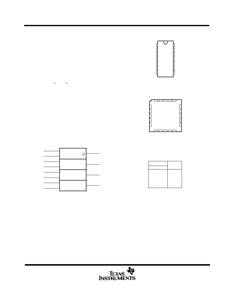
logic symbol
11
= 1
8
6
3
4B
3B
2B
1B
4A
3A
2A
1A
4Y
3Y
2Y
1Y
1
2
4
5
9
10
12
13
This symbol is in accordance with ANSI/IEEE Std 91-1984 and
IEC Publication 617-12.
Pin numbers shown are for D, J, and N packages.
SN54ALS136, SN54AS136 . . . J PACKAGE
SN74ALS136, SN74AS136 . . . D OR N PACKAGE
(TOP VIEW)
SN54ALS136, SN54AS136 . . . FK PACKAGE
(TOP VIEW)
NC No internal connection
FUNCTION TABLE
(each gate)
OUTPUT
INPUTS
A
B
Y
L
L
L
L
L
L
H
H
H
H
H
H
1
2
3
4
5
6
7
14
13
12
11
10
9
8
1A
1B
1Y
2A
2B
2Y
GND
V
CC
4B
4A
4Y
3B
3A
3Y
3
2
1 20 19
9 10 11 12 13
4
5
6
7
8
18
17
16
15
14
4A
NC
4Y
NC
3B
1Y
NC
2A
NC
2B
1B
1A
NC
3Y
3A
4B
2Y
GND
NC
CC
V
SN54ALS136, SN54AS136, SN74ALS136, SN74AS136
QUADRUPLE 2-INPUT EXCLUSIVE-OR GATES
WITH OPEN-COLLECTOR OUTPUTS
SDAS162 MARCH 1984REVISED OCTOBER 1988
POST OFFICE BOX 655303
·
DALLAS, TEXAS 75265
2
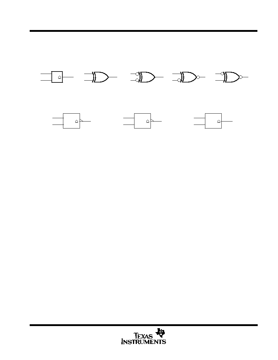
exclusive-OR logic
An Exclusive-OR gate has many applications, some of which can be represented better by alternative logic
symbols.
EXCLUSIVE-OR
= 1
These are five equivalent Exclusive-OR symbols valid for an 'ALS136 gate in positive logic; negation may be
shown at any two ports.
LOGIC IDENTITY ELEMENT
EVEN-PARITY
ODD-PARITY ELEMENT
The output is active (low) if all
inputs stand at the same logic
level (i.e., A=B).
The output is active (low) if an
even number of inputs (i.e., 0 or
2) are active.
The output is active (high if an
odd number of inputs (i.e., only
1 of the 2) are active.
=
2k
2k + 1

UNIT
UNIT
VOL
V
TEST CONDITIONS
PARAMETER
PARAMETER
UNIT
ns
ns
Y
Y
SN54ALS136, SN74ALS136
QUADRUPLE 2-INPUT EXCLUSIVE-OR GATES
WITH OPEN-COLLECTOR OUTPUTS
SDAS162 MARCH 1984REVISED OCTOBER 1988
POST OFFICE BOX 655303
·
DALLAS, TEXAS 75265
3
absolute maximum ratings over operating free-air temperature range (unless otherwise noted)
Supply voltage, V
CC
7 V
. . . . . . . . . . . . . . . . . . . . . . . . . . . . . . . . . . . . . . . . . . . . . . . . . . . . . . . . . . . . . . . . . . . . . . . .
Input voltage
7 V
. . . . . . . . . . . . . . . . . . . . . . . . . . . . . . . . . . . . . . . . . . . . . . . . . . . . . . . . . . . . . . . . . . . . . . . . . . . . . . .
Off-state output voltage
7 V
. . . . . . . . . . . . . . . . . . . . . . . . . . . . . . . . . . . . . . . . . . . . . . . . . . . . . . . . . . . . . . . . . . . . . .
Operating free-air temperature range: SN54ALS136
55
°
C to 125
°
C
. . . . . . . . . . . . . . . . . . . . . . . . . . . . . . . .
SN74ALS136
0
°
C to 70
°
C
. . . . . . . . . . . . . . . . . . . . . . . . . . . . . . . . . . .
Storage temperature range
65
°
C to 150
°
C
. . . . . . . . . . . . . . . . . . . . . . . . . . . . . . . . . . . . . . . . . . . . . . . . . . . . . . . .
recommended operating conditions
SN54ALS136
SN74ALS136
MIN
NOM
MAX
MIN
NOM
MAX
VCC
Supply Voltage
4.5
5
5.5
4.5
5
5.5
V
VIH
High-level input Voltage
2
2
V
VIL
Low-level input voltage
0.7
0.8
V
VOH
High-level output current
5.5
5.5
V
IOL
Low-level output current
4
8
mA
TA
Operating free-air temperature
55
125
0
70
°
C
electrical characteristics over recommended operating free-air temperature range (unless
otherwise noted)
SN54ALS136
SN74ALS136
MIN
TYP
MAX
MIN
TYP
MAX
VIK
VCC = 4.5 V,
II = 18 mA
1.5
1.5
V
IOH
VCC = 4.5 V,
VOH = 5.5 V
0.1
0.1
mA
VCC = 4.5 V,
IOL = 4 mA
0.25
0.4
0.25
0.4
VCC = 4.5 V,
IOL = 8 mA
0.35
0.5
II
VCC = 5.5 V,
VI = 7 V
0.1
0.1
mA
IIH
VCC = 5.5 V,
VI = 2.7 V
20
20
µ
A
IIL
VCC = 5.5 V,
VI = 0.4 V
0.1
0.1
mA
ICC
VCC = 5.5 V
All inputs at 4.5 V
3.9
5.9
3.9
5.9
mA
All typical values are at VCC = 5, TA = 25
°
C.
switching characteristics (see Note 1)
VCC = 4.5 V to 5.5 V,
CL = 50 pF,
FROM
TO
RL = 2 k
,
(INPUT)
(OUTPUT)
TA = MIN to MAX
SN54ALS136
SN74ALS136
MIN
MAX
MIN
MAX
tPLH
A or B
20
55
20
50
tPHL
(other input low)
3
18
3
15
tPLH
A or B
20
55
20
50
tPHL
(other input low)
3
18
3
15
NOTE 1: Load circuit and voltage waveforms are shown in Section 1 of the ALS/AS Logic Data Book, 1986.

UNIT
UNIT
TEST CONDITIONS
PARAMETER
PARAMETER
UNIT
ns
ns
Y
Y
SN54AS136, SN74AS136
QUADRUPLE 2-INPUT EXCLUSIVE-OR GATES
WITH OPEN-COLLECTOR OUTPUTS
SDAS162 MARCH 1984REVISED OCTOBER 1988
POST OFFICE BOX 655303
·
DALLAS, TEXAS 75265
4
absolute maximum ratings over operating free-air temperature range (unless otherwise noted)
Supply voltage, V
CC
7 V
. . . . . . . . . . . . . . . . . . . . . . . . . . . . . . . . . . . . . . . . . . . . . . . . . . . . . . . . . . . . . . . . . . . . . . . .
Input voltage
7 V
. . . . . . . . . . . . . . . . . . . . . . . . . . . . . . . . . . . . . . . . . . . . . . . . . . . . . . . . . . . . . . . . . . . . . . . . . . . . . . .
Off-state output voltage
7 V
. . . . . . . . . . . . . . . . . . . . . . . . . . . . . . . . . . . . . . . . . . . . . . . . . . . . . . . . . . . . . . . . . . . . . .
Operating free-air temperature range: SN54AS136
55
°
C to 125
°
C
. . . . . . . . . . . . . . . . . . . . . . . . . . . . . . . . . .
SN74AS136
0
°
C to 70
°
C
. . . . . . . . . . . . . . . . . . . . . . . . . . . . . . . . . . . . .
Storage temperature range
65
°
C to 150
°
C
. . . . . . . . . . . . . . . . . . . . . . . . . . . . . . . . . . . . . . . . . . . . . . . . . . . . . . . . .
recommended operating conditions
SN54AS136
SN74ALS136
MIN
NOM
MAX
MIN
NOM
MAX
VCC
Supply Voltage
4.5
5
5.5
4.5
5
5.5
V
VIH
High-level input Voltage
2
2
V
VIL
Low-level input voltage
0.8
0.8
V
VOH
High-level output current
5.5
5.5
V
IOL
Low-level output current
20
20
mA
TA
Operating free-air temperature
55
125
0
70
°
C
electrical characteristics over recommended operating free-air temperature range (unless
otherwise noted)
SN54AS136
SN74AS136
MIN
TYP
MAX
MIN
TYP
MAX
VIK
VCC = 4.5 V,
II = 18 mA
1.5
1.5
V
IOH
VCC = 4.5 V,
VOH = 5.5 V
2
0.1
mA
VOL
VCC = 4.5 V,
IOL = 4 mA
0.35
0.5
0.25
0.4
V
II
VCC = 5.5 V,
VI = 7 V
0.1
0.1
mA
IIH
VCC = 5.5 V,
VI = 2.7 V
20
20
µ
A
IIL
VCC = 5.5 V,
VI = 0.4 V
0.5
0.5
mA
ICC
VCC = 5.5 V
VIA = 4.5 V,
VIB = 0
14
20
14
20
mA
ICCL
VCC = 5.5 V
VIA = 4.5 V
22
31
22
31
mA
All typical values are at VCC = 5, TA = 25
°
C.
switching characteristics (see Note 1)
VCC = 4.5 V to 5.5 V,
CL = 50 pF,
FROM
TO
RL = 2 k
,
(INPUT)
(OUTPUT)
TA = MIN to MAX
SN54AS136
SN74ALS136
MIN
MAX
MIN
MAX
tPLH
A or B
6.3
14.8
6.3
12.5
tPHL
(other input low)
3.3
7.9
3.3
7.1
tPLH
A or B
6.3
12.4
6.3
11.4
tPHL
(other input low)
3.3
14.1
3.3
10.7
NOTE 1: Load circuit and voltage waveforms are shown in Section 1 of the ALS/AS Logic Data Book, 1986.

IMPORTANT NOTICE
Texas Instruments and its subsidiaries (TI) reserve the right to make changes to their products or to discontinue
any product or service without notice, and advise customers to obtain the latest version of relevant information
to verify, before placing orders, that information being relied on is current and complete. All products are sold
subject to the terms and conditions of sale supplied at the time of order acknowledgement, including those
pertaining to warranty, patent infringement, and limitation of liability.
TI warrants performance of its semiconductor products to the specifications applicable at the time of sale in
accordance with TI's standard warranty. Testing and other quality control techniques are utilized to the extent
TI deems necessary to support this warranty. Specific testing of all parameters of each device is not necessarily
performed, except those mandated by government requirements.
CERTAIN APPLICATIONS USING SEMICONDUCTOR PRODUCTS MAY INVOLVE POTENTIAL RISKS OF
DEATH, PERSONAL INJURY, OR SEVERE PROPERTY OR ENVIRONMENTAL DAMAGE ("CRITICAL
APPLICATIONS"). TI SEMICONDUCTOR PRODUCTS ARE NOT DESIGNED, AUTHORIZED, OR
WARRANTED TO BE SUITABLE FOR USE IN LIFE-SUPPORT DEVICES OR SYSTEMS OR OTHER
CRITICAL APPLICATIONS. INCLUSION OF TI PRODUCTS IN SUCH APPLICATIONS IS UNDERSTOOD TO
BE FULLY AT THE CUSTOMER'S RISK.
In order to minimize risks associated with the customer's applications, adequate design and operating
safeguards must be provided by the customer to minimize inherent or procedural hazards.
TI assumes no liability for applications assistance or customer product design. TI does not warrant or represent
that any license, either express or implied, is granted under any patent right, copyright, mask work right, or other
intellectual property right of TI covering or relating to any combination, machine, or process in which such
semiconductor products or services might be or are used. TI's publication of information regarding any third
party's products or services does not constitute TI's approval, warranty or endorsement thereof.
Copyright
©
1998, Texas Instruments Incorporated