
SN54AHCT595, SN74AHCT595
8-BIT SHIFT REGISTERS
WITH 3-STATE OUTPUT REGISTERS
SCLS374F MAY 1997 REVISED JANUARY 2000
1
POST OFFICE BOX 655303
·
DALLAS, TEXAS 75265
D
EPIC
TM
(Enhanced-Performance Implanted
CMOS) Process
D
Inputs Are TTL-Voltage Compatible
D
8-Bit Serial-In, Parallel-Out Shift
D
Shift Register Has Direct Clear
D
Latch-Up Performance Exceeds 100 mA Per
JESD 78, Class II
D
ESD Protection Exceeds JESD 22
2000-V Human-Body Model (A114-A)
200-V Machine Model (A115-A)
1000-V Charged-Device Model (C101)
D
Package Options Include Plastic
Small-Outline (D), Shrink Small-Outline
(DB), Thin Shrink Small-Outline (PW), and
Ceramic Flat (W) Packages, Ceramic Chip
Carriers (FK), and Standard Plastic (N) and
Ceramic (J) DIPs
description
The 'AHCT595 devices contain an 8-bit serial-in,
parallel-out shift register that feeds an 8-bit D-type
storage register. The storage register has parallel
3-state outputs. Separate clocks are provided for
the shift and storage registers. The shift register
has a direct overriding clear (SRCLR) input, serial
(SER) input, and serial outputs for cascading.
When the output-enable (OE) input is high, the
outputs are in the high-impedance state.
Both the shift register clock (RCLK) and storage register clock (SRCLK) are positive-edge triggered. If both
clocks are connected together, the shift register always is one clock pulse ahead of the storage register.
The SN54AHCT595 is characterized for operation over the full military temperature range of 55
°
C to 125
°
C.
The SN74AHCT595 is characterized for operation from 40
°
C to 85
°
C.
Copyright
©
2000, Texas Instruments Incorporated
UNLESS OTHERWISE NOTED this document contains PRODUCTION
DATA information current as of publication date. Products conform to
specifications per the terms of Texas Instruments standard warranty.
Production processing does not necessarily include testing of all
parameters.
Please be aware that an important notice concerning availability, standard warranty, and use in critical applications of
Texas Instruments semiconductor products and disclaimers thereto appears at the end of this data sheet.
EPIC is a trademark of Texas Instruments Incorporated.
SN54AHCT595 . . . J OR W PACKAGE
SN74AHCT595 . . . D, DB, N, OR PW PACKAGE
(TOP VIEW)
SN54AHCT595 . . . FK PACKAGE
(TOP VIEW)
NC No internal connection
1
2
3
4
5
6
7
8
16
15
14
13
12
11
10
9
Q
B
Q
C
Q
D
Q
E
Q
F
Q
G
Q
H
GND
V
CC
Q
A
SER
OE
RCLK
SRCLK
SRCLR
Q
H
4
5
6
7
8
18
17
16
15
14
SER
OE
NC
RCLK
SRCLK
Q
D
Q
E
NC
Q
F
Q
G
Q
NC
SRCLR
H
GND
NC
C
Q
B
V
CC
Q
A
Q
H
Q
9 10 11 12 13
3
2
1 20 19

SN54AHCT595, SN74AHCT595
8-BIT SHIFT REGISTERS
WITH 3-STATE OUTPUT REGISTERS
SCLS374F MAY 1997 REVISED JANUARY 2000
2
POST OFFICE BOX 655303
·
DALLAS, TEXAS 75265
FUNCTION TABLE
INPUTS
FUNCTION
SER
SRCLK
SRCLR
RCLK
OE
FUNCTION
X
X
X
X
H
Outputs QAQH are disabled.
X
X
X
X
L
Outputs QAQH are enabled.
X
X
L
X
X
Shift register is cleared.
L
H
X
X
First stage of the shift register goes low.
Other stages store the data of previous stage, respectively.
H
H
X
X
First stage of the shift register goes high.
Other stages store the data of previous stage, respectively.
X
H
X
X
Shift-register state is not changed.
X
X
X
X
Shift-register data is stored into the storage register.
X
X
X
X
Storage-register state is not changed.
logic symbol
R
10
15
1
2
3
11
SRCLK
EN3
13
12
RCLK
C2
4
5
6
7
2D
This symbol is in accordance with ANSI/IEEE Std 91-1984 and IEC Publication 617-12.
Pin numbers shown are for the D, DB, J, N, PW, and W packages.
SRG8
OE
SRCLR
QA
QB
QC
QD
QE
QF
QG
QH
1D
14
SER
C1/
2D
9
QH
3
3

SN54AHCT595, SN74AHCT595
8-BIT SHIFT REGISTERS
WITH 3-STATE OUTPUT REGISTERS
SCLS374F MAY 1997 REVISED JANUARY 2000
3
POST OFFICE BOX 655303
·
DALLAS, TEXAS 75265
logic diagram (positive logic)
3D
C3
1D
C1
R
3D
C3
2D
C2
R
3D
C3
2D
C2
R
3D
C3
2D
C2
R
3D
C3
2D
C2
R
3D
C3
2D
C2
R
3D
C3
2D
C2
R
3D
C3
2D
C2
R
13
12
10
11
14
15
1
2
3
4
5
6
7
9
QA
QB
QC
QD
QE
QF
QG
QH
QH
OE
SRCLR
RCLK
SRCLK
SER
Pin numbers shown are for the D, DB, J, N, PW, and W packages.
Q
Q
Q
Q
Q
Q
Q
Q
Q
Q
Q
Q
Q
Q
Q
Q

SN54AHCT595, SN74AHCT595
8-BIT SHIFT REGISTERS
WITH 3-STATE OUTPUT REGISTERS
SCLS374F MAY 1997 REVISED JANUARY 2000
4
POST OFFICE BOX 655303
·
DALLAS, TEXAS 75265
timing diagram
SRCLK
SER
RCLK
SRCLR
OE
ÎÎÎÎÎ
ÎÎÎÎÎ
QA
ÎÎÎÎÎ
ÎÎÎÎÎ
QB
ÎÎÎÎÎ
ÎÎÎÎÎ
QC
ÎÎÎÎÎ
ÎÎÎÎÎ
QD
ÎÎÎÎÎ
ÎÎÎÎÎ
QE
ÎÎÎÎÎ
ÎÎÎÎÎ
QF
ÎÎÎÎÎ
ÎÎÎÎÎ
QG
ÎÎÎÎÎ
ÎÎÎÎÎ
QH
QH'
SN54AHCT595, SN74AHCT595
8-BIT SHIFT REGISTERS
WITH 3-STATE OUTPUT REGISTERS
SCLS374F MAY 1997 REVISED JANUARY 2000
5
POST OFFICE BOX 655303
·
DALLAS, TEXAS 75265
absolute maximum ratings over operating free-air temperature range (unless otherwise noted)
Supply voltage range, V
CC
0.5 V to 7 V
. . . . . . . . . . . . . . . . . . . . . . . . . . . . . . . . . . . . . . . . . . . . . . . . . . . . . . . . . .
Input voltage range, V
I
(see Note 1)
0.5 V to 7 V
. . . . . . . . . . . . . . . . . . . . . . . . . . . . . . . . . . . . . . . . . . . . . . . . . .
Output voltage range, V
O
(see Note 1)
0.5 V to V
CC
+ 0.5 V
. . . . . . . . . . . . . . . . . . . . . . . . . . . . . . . . . . . . . . . .
Input clamp current, I
IK
(V
I
< 0)
20 mA
. . . . . . . . . . . . . . . . . . . . . . . . . . . . . . . . . . . . . . . . . . . . . . . . . . . . . . . . . . .
Output clamp current, I
OK
(V
O
< 0 or V
O
> V
CC
)
±
20 mA
. . . . . . . . . . . . . . . . . . . . . . . . . . . . . . . . . . . . . . . . . . . .
Continuous output current, I
O
(V
O
= 0 to V
CC
)
±
25 mA
. . . . . . . . . . . . . . . . . . . . . . . . . . . . . . . . . . . . . . . . . . . . . .
Continuous current through V
CC
or GND
±
50 mA
. . . . . . . . . . . . . . . . . . . . . . . . . . . . . . . . . . . . . . . . . . . . . . . . . . .
Package thermal impedance,
JA
(see Note 2): D package
73
°
C/W
. . . . . . . . . . . . . . . . . . . . . . . . . . . . . . . . . . .
DB package
82
°
C/W
. . . . . . . . . . . . . . . . . . . . . . . . . . . . . . . . .
N package
67
°
C/W
. . . . . . . . . . . . . . . . . . . . . . . . . . . . . . . . . . .
PW package
108
°
C/W
. . . . . . . . . . . . . . . . . . . . . . . . . . . . . . . .
Storage temperature range, T
stg
65
°
C to 150
°
C
. . . . . . . . . . . . . . . . . . . . . . . . . . . . . . . . . . . . . . . . . . . . . . . . . . .
Stresses beyond those listed under "absolute maximum ratings" may cause permanent damage to the device. These are stress ratings only, and
functional operation of the device at these or any other conditions beyond those indicated under "recommended operating conditions" is not
implied. Exposure to absolute-maximum-rated conditions for extended periods may affect device reliability.
NOTES:
1. The input and output voltage ratings may be exceeded if the input and output current ratings are observed.
2. The package thermal impedance is calculated in accordance with JESD 51.
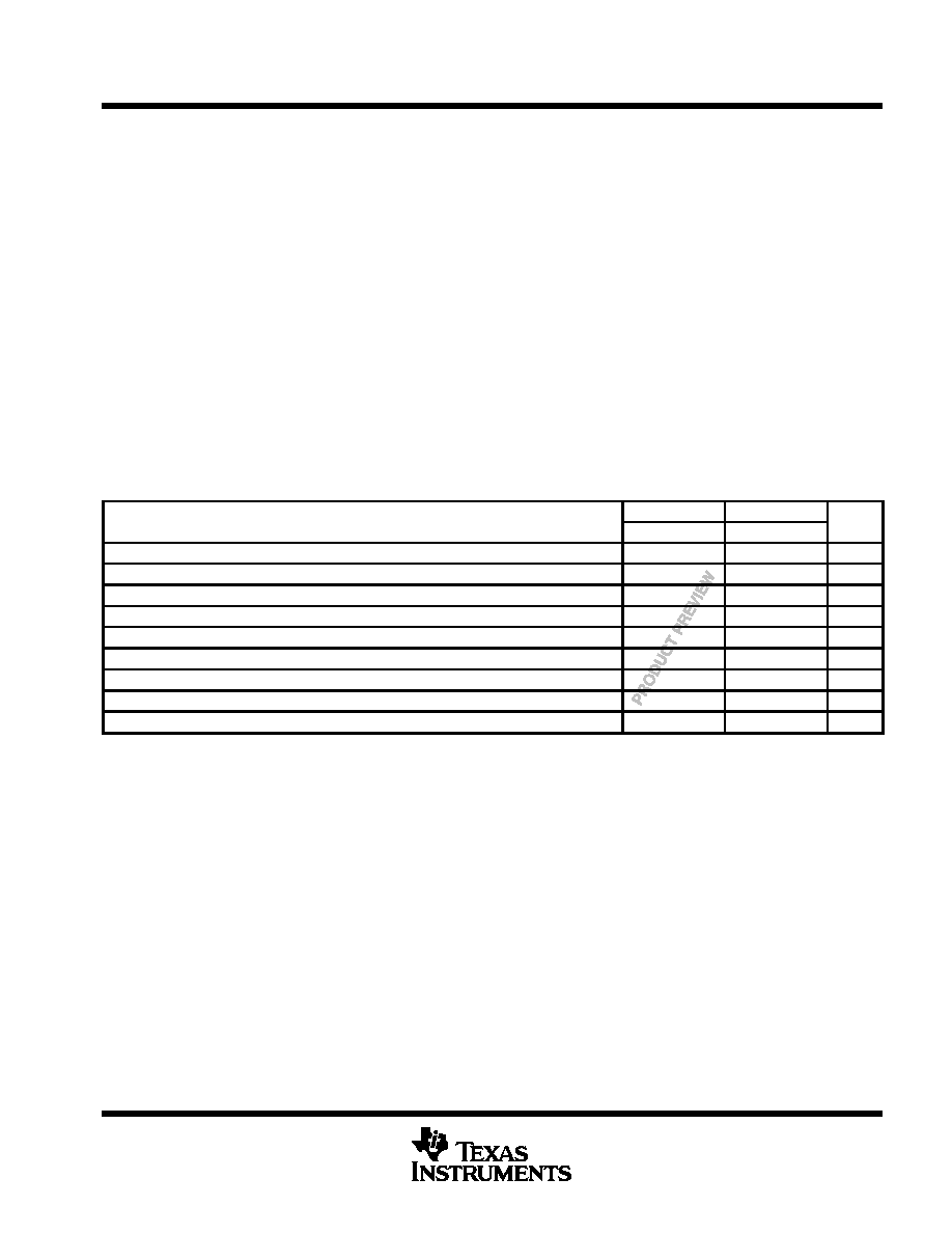
recommended operating conditions (see Note 3)
SN54AHCT595
SN74AHCT595
UNIT
MIN
MAX
MIN
MAX
UNIT
VCC
Supply voltage
4.5
5.5
4.5
5.5
V
VIH
High-level input voltage
2
2
V
VIL
Low-level input voltage
0.8
0.8
V
VI
Input voltage
0
5.5
0
5.5
V
VO
Output voltage
0
VCC
0
VCC
V
IOH
High-level output current
8
8
mA
IOL
Low-level output current
8
8
mA
t/
v
Input transition rise or fall rate
20
20
ns/V
TA
Operating free-air temperature
55
125
40
85
°
C
NOTE 3: All unused inputs of the device must be held at VCC or GND to ensure proper device operation. Refer to the TI application report,
Implications of Slow or Floating CMOS Inputs, literature number SCBA004.
PRODUCT PREVIEW information concerns products in the formative or
design phase of development. Characteristic data and other
specifications are design goals. Texas Instruments reserves the right to
change or discontinue these products without notice.