SN54AHCT594, SN74AHCT594
8-BIT SHIFT REGISTERS
WITH OUTPUT REGISTERS
SCLS417F JUNE 1998 REVISED NOVEMBER 2002
1
POST OFFICE BOX 655303
·
DALLAS, TEXAS 75265
D
Inputs Are TTL-Voltage Compatible
D
8-Bit Serial-In, Parallel-Out Shift
Registers With Storage
D
Independent Direct Overriding Clears
on Shift and Storage Registers
D
Independent Clocks for Both Shift and
Storage Registers
D
Latch-Up Performance Exceeds 100 mA
Per JESD 78, Class II
D
ESD Protection Exceeds JESD 22
2000-V Human-Body Model (A114-A)
200-V Machine Model (A115-A)
1000-V Charged-Device Model (C101)
description/ordering information
The 'AHCT594 devices contain an 8-bit serial-in,
parallel-out shift register that feeds an 8-bit D-type
storage register. Separate clocks and direct
overriding clear (SRCLR, RCLR) inputs are
provided on both the shift and storage registers.
A serial (Q
H
) output is provided for cascading
purposes.
Both the shift register (SRCLK) and storage
register (RCLK) clocks are positive edge
triggered. If both clocks are connected together,
the shift register always is one count pulse ahead
of the storage register.
ORDERING INFORMATION
TA
PACKAGE
ORDERABLE
PART NUMBER
TOP-SIDE
MARKING
PDIP N
Tube
SN74AHCT594N
SN74AHCT594N
SOIC
D
Tube
SN74AHCT594D
AHCT594
40
°
C to 85
°
C
SOIC D
Tape and reel
SN74AHCT594DR
AHCT594
40
°
C to 85
°
C
SOP NS
Tape and reel
SN74AHCT594NSR
AHCT594
SSOP DB
Tape and reel
SN74AHCT594DBR
HB594
TSSOP PW
Tape and reel
SN74AHCT594PWR
HB594
CDIP J
Tube
SNJ54AHCT594J
SNJ54AHCT594J
55
°
C to 125
°
C
CFP W
Tube
SNJ54AHCT594W
SNJ54AHCT594W
LCCC FK
Tube
SNJ54AHCT594FK
SNJ54AHCT594FK
Package drawings, standard packing quantities, thermal data, symbolization, and PCB design guidelines
are available at www.ti.com/sc/package.
UNLESS OTHERWISE NOTED this document contains PRODUCTION
DATA information current as of publication date. Products conform to
specifications per the terms of Texas Instruments standard warranty.
Production processing does not necessarily include testing of all
parameters.
Copyright
2002, Texas Instruments Incorporated
Please be aware that an important notice concerning availability, standard warranty, and use in critical applications of
Texas Instruments semiconductor products and disclaimers thereto appears at the end of this data sheet.
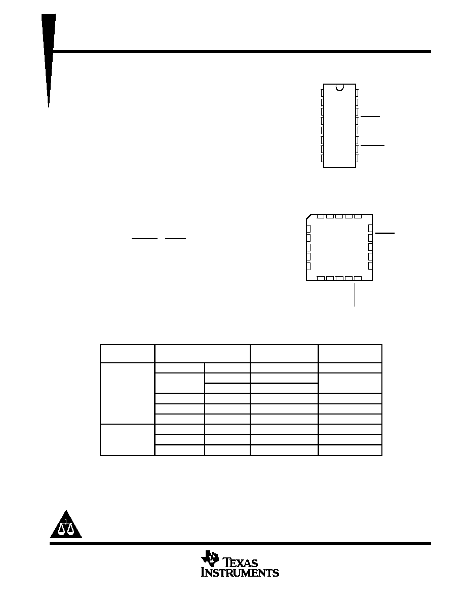
SN54AHCT594 . . . J OR W PACKAGE
SN74AHCT594 . . . D, DB, N, NS, OR PW PACKAGE
(TOP VIEW)
SN54AHCT594 . . . FK PACKAGE
(TOP VIEW)
NC No internal connection
1
2
3
4
5
6
7
8
16
15
14
13
12
11
10
9
Q
B
Q
C
Q
D
Q
E
Q
F
Q
G
Q
H
GND
V
CC
Q
A
SER
RCLR
RCLK
SRCLK
SRCLR
Q
H
3
2 1 20 19
9 10 11 12 13
4
5
6
7
8
18
17
16
15
14
SER
RCLR
NC
RCLK
SRCLK
Q
D
Q
E
NC
Q
F
Q
G
Q
NC
SRCLR
H
GND
NC
C
Q
B
V
CC
Q
A
Q
H
Q

SN54AHCT594, SN74AHCT594
8-BIT SHIFT REGISTERS
WITH OUTPUT REGISTERS
SCLS417F JUNE 1998 REVISED NOVEMBER 2002
2
POST OFFICE BOX 655303
·
DALLAS, TEXAS 75265
FUNCTION TABLE
INPUTS
FUNCTION
SER
SRCLK
SRCLR
RCLK
RCLR
FUNCTION
X
X
L
X
X
Shift register is cleared.
L
H
X
X
First stage of shift register goes low.
Other stages store the data of previous stage, respectively.
H
H
X
X
First stage of shift register goes high.
Other stages store the data of previous stage, respectively.
L
H
X
X
Shift-register state is not changed.
X
X
X
X
L
Storage register is cleared.
X
X
X
H
Shift-register data is stored in the storage register.
X
X
X
H
Storage-register state is not changed.

SN54AHCT594, SN74AHCT594
8-BIT SHIFT REGISTERS
WITH OUTPUT REGISTERS
SCLS417F JUNE 1998 REVISED NOVEMBER 2002
3
POST OFFICE BOX 655303
·
DALLAS, TEXAS 75265
logic diagram (positive logic)
R
3D
C3
1D
C1
R
R
3D
C3
2D
C2
R
R
3D
C3
2D
C2
R
R
3D
C3
2D
C2
R
R
3D
C3
2D
C2
R
R
3D
C3
2D
C2
R
R
3D
C3
2D
C2
R
R
3D
C3
2D
C2
R
13
12
10
11
14
15
1
2
3
4
5
6
7
9
QA
QB
QC
QD
QE
QF
QG
QH
QH
RCLR
SRCLR
RCLK
SRCLK
SER
Pin numbers shown are for the D, DB, J, N, NS, PW, and W packages.
Q
Q
Q
Q
Q
Q
Q
Q
Q
Q
Q
Q
Q
Q
Q
Q

SN54AHCT594, SN74AHCT594
8-BIT SHIFT REGISTERS
WITH OUTPUT REGISTERS
SCLS417F JUNE 1998 REVISED NOVEMBER 2002
4
POST OFFICE BOX 655303
·
DALLAS, TEXAS 75265
timing diagram
SRCLK
SER
RCLK
SRCLR
RCLR
ÎÎÎÎÎ
ÎÎÎÎÎ
QA
ÎÎÎÎÎ
ÎÎÎÎÎ
QB
ÎÎÎÎÎ
ÎÎÎÎÎ
QC
ÎÎÎÎÎ
ÎÎÎÎÎ
QD
ÎÎÎÎÎ
ÎÎÎÎÎ
QE
ÎÎÎÎÎ
ÎÎÎÎÎ
QF
ÎÎÎÎÎ
ÎÎÎÎÎ
QG
ÎÎÎÎÎ
ÎÎÎÎÎ
QH
QH'

SN54AHCT594, SN74AHCT594
8-BIT SHIFT REGISTERS
WITH OUTPUT REGISTERS
SCLS417F JUNE 1998 REVISED NOVEMBER 2002
5
POST OFFICE BOX 655303
·
DALLAS, TEXAS 75265
absolute maximum ratings over operating free-air temperature range (unless otherwise noted)
Supply voltage range, V
CC
0.5 V to 7 V
. . . . . . . . . . . . . . . . . . . . . . . . . . . . . . . . . . . . . . . . . . . . . . . . . . . . . . . . . .
Input voltage range, V
I
(see Note 1)
0.5 V to 7 V
. . . . . . . . . . . . . . . . . . . . . . . . . . . . . . . . . . . . . . . . . . . . . . . . . .
Output voltage range, V
O
(see Note 1)
0.5 V to V
CC
+ 0.5 V
. . . . . . . . . . . . . . . . . . . . . . . . . . . . . . . . . . . . . . . .
Input clamp current, I
IK
(V
I
< 0)
20 mA
. . . . . . . . . . . . . . . . . . . . . . . . . . . . . . . . . . . . . . . . . . . . . . . . . . . . . . . . . . .
Output clamp current, I
OK
(V
O
< 0 or V
O
> V
CC
)
±
20 mA
. . . . . . . . . . . . . . . . . . . . . . . . . . . . . . . . . . . . . . . . . . . .
Continuous output current, I
O
(V
O
= 0 to V
CC
)
±
25 mA
. . . . . . . . . . . . . . . . . . . . . . . . . . . . . . . . . . . . . . . . . . . . . .
Continuous current through V
CC
or GND
±
75 mA
. . . . . . . . . . . . . . . . . . . . . . . . . . . . . . . . . . . . . . . . . . . . . . . . . . .
Package thermal impedance,
JA
(see Note 2): D package
73
°
C/W
. . . . . . . . . . . . . . . . . . . . . . . . . . . . . . . . . . .
DB package
82
°
C/W
. . . . . . . . . . . . . . . . . . . . . . . . . . . . . . . . .
N package
67
°
C/W
. . . . . . . . . . . . . . . . . . . . . . . . . . . . . . . . . . .
NS package
64
°
C/W
. . . . . . . . . . . . . . . . . . . . . . . . . . . . . . . . .
PW package
108
°
C/W
. . . . . . . . . . . . . . . . . . . . . . . . . . . . . . . .
Storage temperature range, T
stg
65
°
C to 150
°
C
. . . . . . . . . . . . . . . . . . . . . . . . . . . . . . . . . . . . . . . . . . . . . . . . . . .
Stresses beyond those listed under "absolute maximum ratings" may cause permanent damage to the device. These are stress ratings only, and
functional operation of the device at these or any other conditions beyond those indicated under "recommended operating conditions" is not
implied. Exposure to absolute-maximum-rated conditions for extended periods may affect device reliability.
NOTES:
1. The input and output voltage ratings may be exceeded if the input and output current ratings are observed.
2. The package thermal impedance is calculated in accordance with JESD 51-7.
recommended operating conditions (see Note 3)
SN54AHCT594
SN74AHCT594
UNIT
MIN
MAX
MIN
MAX
UNIT
VCC
Supply voltage
4.5
5.5
4.5
5.5
V
VIH
High-level input voltage
2
2
V
VIL
Low-level input voltage
0.8
0.8
V
VI
Input voltage
0
5.5
0
5.5
V
VO
Output voltage
0
VCC
0
VCC
V
IOH
High-level output current
8
8
mA
IOL
Low-level output current
8
8
mA
D
t/
D
v
Input transition rise or fall rate
20
20
ns/V
TA
Operating free-air temperature
55
125
40
85
°
C
NOTE 3: All unused inputs of the device must be held at VCC or GND to ensure proper device operation. Refer to the TI application report,
Implications of Slow or Floating CMOS Inputs, literature number SCBA004.
PRODUCT PREVIEW information concerns products in the formative or
design phase of development. Characteristic data and other
specifications are design goals. Texas Instruments reserves the right to
change or discontinue these products without notice.