SN74AHC00-EP
QUADRUPLE 2-INPUT POSITIVE-NAND GATE
SGDS026 JULY 2002
1
POST OFFICE BOX 655303
·
DALLAS, TEXAS 75265
D
Controlled Baseline
One Assembly/Test Site, One Fabrication
Site
D
Extended Temperature Performance of
55
°
C to 125
°
C
D
Enhanced Diminishing Manufacturing
Sources (DMS) Support
D
Enhanced Product Change Notification
D
Qualification Pedigree
D
EPIC
(Enhanced-Performance Implanted
CMOS) Process
Component qualification in accordance with JEDEC and industry
standards to ensure reliable operation over an extended
temperature range. This includes, but is not limited to, Highly
Accelerated Stress Test (HAST) or biased 85/85, temperature
cycle, autoclave or unbiased HAST, electromigration, bond
intermetallic life, and mold compound life.
D
Operating Range 2-V to 5.5-V V
CC
D
ESD Protection Exceeds 2000 V Per
MIL-STD-883, Method 3015; Exceeds 200 V
Using Machine Model (C = 200 pF, R = 0)
description
The SN74AHC00 performs the Boolean function Y
+
A
·
B or Y
+
A
)
B in positive logic.
ORDERING INFORMATION
TA
PACKAGE
ORDERABLE
PART NUMBER
TOP-SIDE
MARKING
55
°
C to 125
°
C
SOIC D
Tape and reel
SN74AHC00MDREP
AHC00MEP
55
°
C to 125
°
C
TSSOP PW
Tape and reel
SN74AHC00MPWREP
HA00MEP
Package drawings, standard packing quantities, thermal data, symbolization, and PCB design guidelines
are available at www.ti.com/sc/package.
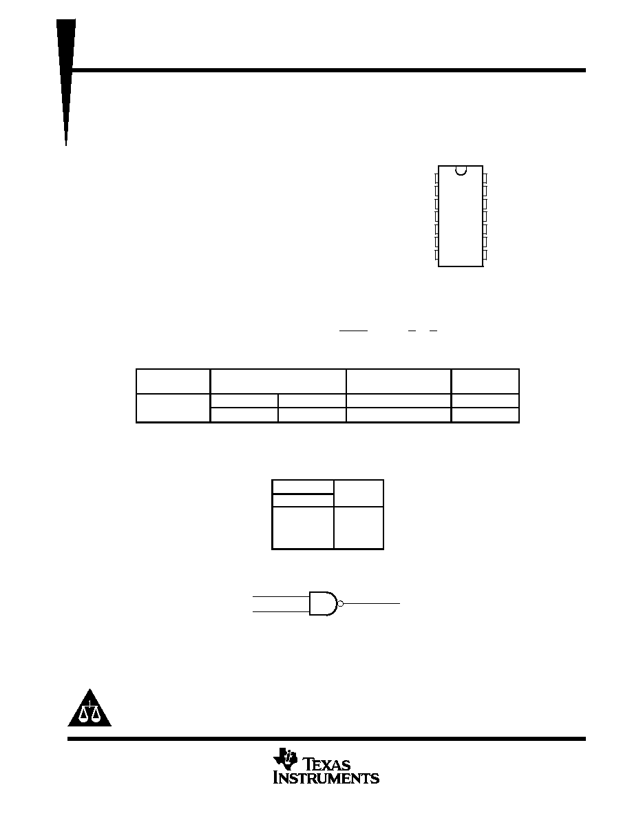
FUNCTION TABLE
(each gate)
INPUTS
OUTPUT
A
B
Y
H
H
L
L
X
H
X
L
H
logic diagram, each gate (positive logic)
A
B
Y
Please be aware that an important notice concerning availability, standard warranty, and use in critical applications of
Texas Instruments semiconductor products and disclaimers thereto appears at the end of this data sheet.
PRODUCTION DATA information is current as of publication date.
Products conform to specifications per the terms of Texas Instruments
standard warranty. Production processing does not necessarily include
testing of all parameters.
Copyright
2002, Texas Instruments Incorporated
EPIC is a trademark of Texas Instruments.
1
2
3
4
5
6
7
14
13
12
11
10
9
8
1A
1B
1Y
2A
2B
2Y
GND
V
CC
4B
4A
4Y
3B
3A
3Y
D OR PW PACKAGE
(TOP VIEW)

SN74AHC00-EP
QUADRUPLE 2-INPUT POSITIVE-NAND GATE
SGDS026 JULY 2002
2
POST OFFICE BOX 655303
·
DALLAS, TEXAS 75265
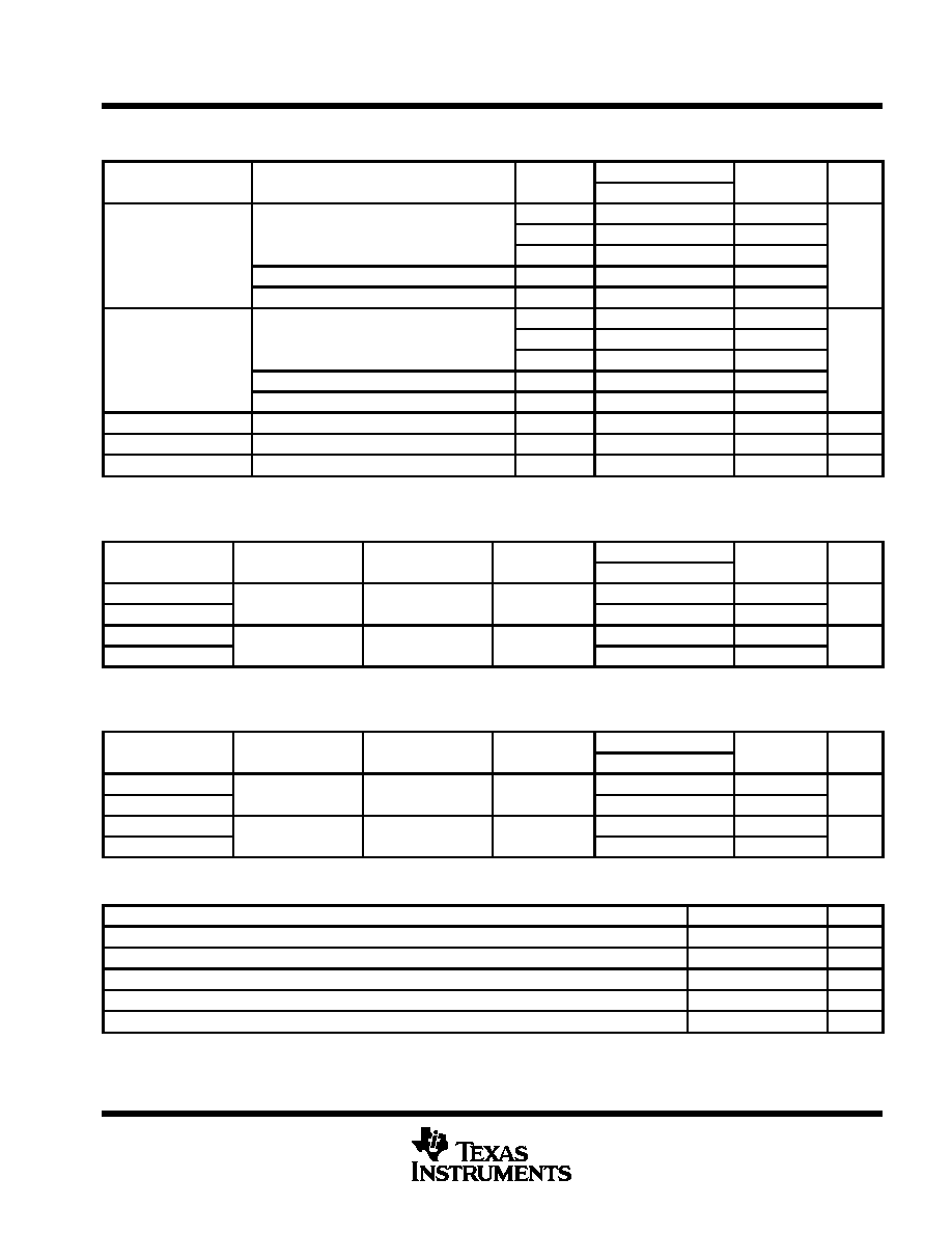
absolute maximum ratings over operating free-air temperature range (unless otherwise noted)
Supply voltage range, V
CC
0.5 V to 7 V
. . . . . . . . . . . . . . . . . . . . . . . . . . . . . . . . . . . . . . . . . . . . . . . . . . . . . . . . . .
Input voltage range, V
I
(see Note 1)
0.5 V to 7 V
. . . . . . . . . . . . . . . . . . . . . . . . . . . . . . . . . . . . . . . . . . . . . . . . . .
Output voltage range, V
O
(see Note 1)
0.5 V to V
CC
+ 0.5 V
. . . . . . . . . . . . . . . . . . . . . . . . . . . . . . . . . . . . . . . .
Input clamp current, I
IK
(V
I
< 0)
20 mA
. . . . . . . . . . . . . . . . . . . . . . . . . . . . . . . . . . . . . . . . . . . . . . . . . . . . . . . . . . .
Output clamp current, I
OK
(V
O
< 0 or V
O
> V
CC
)
±
20 mA
. . . . . . . . . . . . . . . . . . . . . . . . . . . . . . . . . . . . . . . . . . . .
Continuous output current, I
O
(V
O
= 0 to V
CC
)
±
25 mA
. . . . . . . . . . . . . . . . . . . . . . . . . . . . . . . . . . . . . . . . . . . . . .
Continuous current through V
CC
or GND
±
50 mA
. . . . . . . . . . . . . . . . . . . . . . . . . . . . . . . . . . . . . . . . . . . . . . . . . . .
Package thermal impedance,
JA
(see Note 2): D package
86
°
C/W
. . . . . . . . . . . . . . . . . . . . . . . . . . . . . . . . . . .
PW package
113
°
C/W
. . . . . . . . . . . . . . . . . . . . . . . . . . . . . . . .
Storage temperature range, T
stg
65
°
C to 150
°
C
. . . . . . . . . . . . . . . . . . . . . . . . . . . . . . . . . . . . . . . . . . . . . . . . . . .
Stresses beyond those listed under "absolute maximum ratings" may cause permanent damage to the device. These are stress ratings only, and
functional operation of the device at these or any other conditions beyond those indicated under "recommended operating conditions" is not
implied. Exposure to absolute-maximum-rated conditions for extended periods may affect device reliability.
NOTES:
1. The input and output voltage ratings may be exceeded if the input and output current ratings are observed.
2. The package thermal impedance is calculated in accordance with JESD 51-7.
recommended operating conditions (see Note 3)
MIN
MAX
UNIT
VCC
Supply voltage
2
5.5
V
VCC = 2 V
1.5
VIH
High-level input voltage
VCC = 3 V
2.1
V
VCC = 5.5 V
3.85
VCC = 2 V
0.5
VIL
Low-level input voltage
VCC = 3 V
0.9
V
VCC = 5.5 V
1.65
VI
Input voltage
0
5.5
V
VO
Output voltage
0
VCC
V
VCC = 2 V
50
m
A
IOH
High-level output current
VCC = 3.3 V
±
0.3 V
4
mA
VCC = 5 V
±
0.5 V
8
mA
VCC = 2 V
50
m
A
IOL
Low-level output current
VCC = 3.3 V
±
0.3 V
4
mA
VCC = 5 V
±
0.5 V
8
mA
t/
v
Input transition rise or fall rate
VCC = 3.3 V
±
0.3 V
100
ns/V
t/
v
Input transition rise or fall rate
VCC = 5 V
±
0.5 V
20
ns/V
TA
Operating free-air temperature
55
125
°
C
NOTE 3: All unused inputs of the device must be held at VCC or GND to ensure proper device operation. Refer to the TI application report,
Implications of Slow or Floating CMOS Inputs, literature number SCBA004.
SN74AHC00-EP
QUADRUPLE 2-INPUT POSITIVE-NAND GATE
SGDS026 JULY 2002
3
POST OFFICE BOX 655303
·
DALLAS, TEXAS 75265
electrical characteristics over recommended operating free-air temperature range (unless
otherwise noted)
PARAMETER
TEST CONDITIONS
VCC
TA = 25
°
C
MIN
MAX
UNIT
PARAMETER
TEST CONDITIONS
VCC
MIN
TYP
MAX
MIN
MAX
UNIT
2 V
1.9
2
1.9
IOH = 50
m
A
3 V
2.9
3
2.9
VOH
4.5 V
4.4
4.5
4.4
V
IOH = 4 mA
3 V
2.58
2.48
IOH = 8 mA
4.5 V
3.94
3.8
2 V
0.1
0.1
IOL = 50
m
A
3 V
0.1
0.1
VOL
4.5 V
0.1
0.1
V
IOL = 4 mA
3 V
0.36
0.5
IOL = 8 mA
4.5 V
0.36
0.5
II
VI = 5.5 V or GND
0 V to 5.5 V
±
0.1
±
1
m
A
ICC
VI = VCC or GND,
IO = 0
5.5 V
2
20
m
A
Ci
VI = VCC or GND
5 V
2
10
pF
switching characteristics over recommended operating free-air temperature range,
V
CC
= 3.3 V
±
0.3 V (unless otherwise noted) (see Figure 1)
PARAMETER
FROM
TO
LOAD
TA = 25
°
C
MIN
MAX
UNIT
PARAMETER
(INPUT)
(OUTPUT)
CAPACITANCE
MIN
TYP
MAX
MIN
MAX
UNIT
tPLH
A or B
Y
CL = 15 pF
5.5
7.9
1
9.5
ns
tPHL
A or B
Y
CL = 15 pF
5.5
7.9
1
9.5
ns
tPLH
A or B
Y
CL = 50 pF
8
11.4
1
13
ns
tPHL
A or B
Y
CL = 50 pF
8
11.4
1
13
ns
switching characteristics over recommended operating free-air temperature range,
V
CC
= 5 V
±
0.5 V (unless otherwise noted) (see Figure 1)
PARAMETER
FROM
TO
LOAD
TA = 25
°
C
MIN
MAX
UNIT
PARAMETER
(INPUT)
(OUTPUT)
CAPACITANCE
MIN
TYP
MAX
MIN
MAX
UNIT
tPLH
A or B
Y
CL = 15 pF
3.7
5.5
1
6.5
ns
tPHL
A or B
Y
CL = 15 pF
3.7
5.5
1
6.5
ns
tPLH
A or B
Y
CL = 50 pF
5.2
7.5
1
8.5
ns
tPHL
A or B
Y
CL = 50 pF
5.2
7.5
1
8.5
ns
noise characteristics, V
CC
= 5 V, C
L
= 50 pF, T
A
= 25
°
C (see Note 4)
PARAMETER
MIN
TYP
MAX
UNIT
VOL(P)
Quiet output, maximum dynamic VOL
0.3
0.8
V
VOL(V)
Quiet output, minimum dynamic VOL
0.3
0.8
V
VOH(V)
Quiet output, minimum dynamic VOH
4.6
V
VIH(D)
High-level dynamic input voltage
3.5
V
VIL(D)
Low-level dynamic input voltage
1.5
V
NOTE 4: Characteristics are for surface-mount packages only.
SN74AHC00-EP
QUADRUPLE 2-INPUT POSITIVE-NAND GATE
SGDS026 JULY 2002
4
POST OFFICE BOX 655303
·
DALLAS, TEXAS 75265
operating characteristics, V
CC
= 5 V, T
A
= 25
°
C
PARAMETER
TEST CONDITIONS
TYP
UNIT
Cpd
Power dissipation capacitance
No load,
f = 1 MHz
9.5
pF
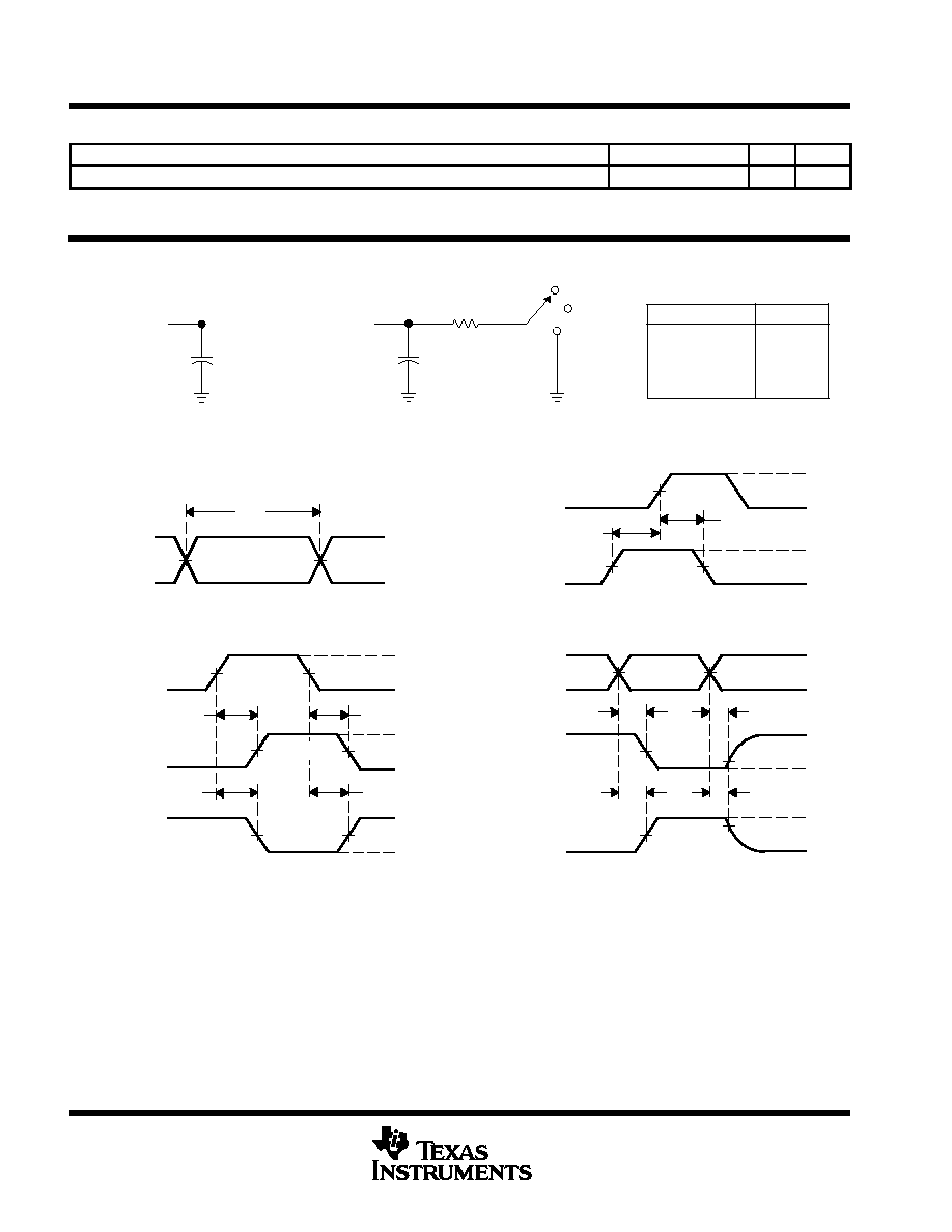
PARAMETER MEASUREMENT INFORMATION
50% VCC
VCC
VCC
0 V
0 V
th
tsu
VOLTAGE WAVEFORMS
SETUP AND HOLD TIMES
Data Input
tPLH
tPHL
tPHL
tPLH
VOH
VOH
VOL
VOL
VCC
0 V
50% VCC
50% VCC
Input
Out-of-Phase
Output
In-Phase
Output
Timing Input
50% VCC
VOLTAGE WAVEFORMS
PROPAGATION DELAY TIMES
INVERTING AND NONINVERTING OUTPUTS
Output
Control
Output
Waveform 1
S1 at VCC
(see Note B)
Output
Waveform 2
S1 at GND
(see Note B)
VOL
VOH
tPZL
tPZH
tPLZ
tPHZ
VCC
0 V
50% VCC
VOL
+ 0.3 V
50% VCC
0 V
VCC
VOLTAGE WAVEFORMS
ENABLE AND DISABLE TIMES
LOW- AND HIGH-LEVEL ENABLING
tPLH/tPHL
tPLZ/tPZL
tPHZ/tPZH
Open Drain
Open
VCC
GND
VCC
TEST
S1
VCC
0 V
50% VCC
tw
VOLTAGE WAVEFORMS
PULSE DURATION
Input
NOTES: A. CL includes probe and jig capacitance.
B. Waveform 1 is for an output with internal conditions such that the output is low except when disabled by the output control.
Waveform 2 is for an output with internal conditions such that the output is high except when disabled by the output control.
C. All input pulses are supplied by generators having the following characteristics: PRR
1 MHz, ZO = 50
, tr
3 ns, tf
3 ns.
D. The outputs are measured one at a time with one input transition per measurement.
From Output
Under Test
CL
(see Note A)
LOAD CIRCUIT FOR
3-STATE AND OPEN-DRAIN OUTPUTS
S1
VCC
RL = 1 k
GND
From Output
Under Test
CL
(see Note A)
Test
Point
LOAD CIRCUIT FOR
TOTEM-POLE OUTPUTS
Open
50% VCC
50% VCC
50% VCC
50% VCC
50% VCC
50% VCC
50% VCC
50% VCC
VOH
0.3 V
Figure 1. Load Circuit and Voltage Waveforms

IMPORTANT NOTICE
Texas Instruments Incorporated and its subsidiaries (TI) reserve the right to make corrections, modifications,
enhancements, improvements, and other changes to its products and services at any time and to discontinue
any product or service without notice. Customers should obtain the latest relevant information before placing
orders and should verify that such information is current and complete. All products are sold subject to TI's terms
and conditions of sale supplied at the time of order acknowledgment.
TI warrants performance of its hardware products to the specifications applicable at the time of sale in
accordance with TI's standard warranty. Testing and other quality control techniques are used to the extent TI
deems necessary to support this warranty. Except where mandated by government requirements, testing of all
parameters of each product is not necessarily performed.
TI assumes no liability for applications assistance or customer product design. Customers are responsible for
their products and applications using TI components. To minimize the risks associated with customer products
and applications, customers should provide adequate design and operating safeguards.
TI does not warrant or represent that any license, either express or implied, is granted under any TI patent right,
copyright, mask work right, or other TI intellectual property right relating to any combination, machine, or process
in which TI products or services are used. Information published by TI regarding thirdparty products or services
does not constitute a license from TI to use such products or services or a warranty or endorsement thereof.
Use of such information may require a license from a third party under the patents or other intellectual property
of the third party, or a license from TI under the patents or other intellectual property of TI.
Reproduction of information in TI data books or data sheets is permissible only if reproduction is without
alteration and is accompanied by all associated warranties, conditions, limitations, and notices. Reproduction
of this information with alteration is an unfair and deceptive business practice. TI is not responsible or liable for
such altered documentation.
Resale of TI products or services with statements different from or beyond the parameters stated by TI for that
product or service voids all express and any implied warranties for the associated TI product or service and
is an unfair and deceptive business practice. TI is not responsible or liable for any such statements.
Mailing Address:
Texas Instruments
Post Office Box 655303
Dallas, Texas 75265
Copyright
2002, Texas Instruments Incorporated