SN54ACT74, SN74ACT74
DUAL POSITIVE-EDGE-TRIGGERED D-TYPE FLIP-FLOPS
WITH CLEAR AND PRESET
SCAS520E ¡ AUGUST 1995 ¡ REVISED JANUARY 2000
1
POST OFFICE BOX 655303
À
DALLAS, TEXAS 75265
D
Inputs Are TTL-Voltage Compatible
D
EPIC
TM
(Enhanced-Performance Implanted
CMOS) 1-
Á
m Process
D
Package Options Include Plastic
Small-Outline (DW) Shrink Small-Outline
(DB), and Thin Shrink Small-Outline (PW)
Packages, Ceramic Chip Carriers (FK) and
Flatpacks (W), and Standard Plastic (N) and
Ceramic (J) DIPs
description
The 'ACT74 dual positive-edge-triggered devices
are D-type flip-flops.
A low level at the preset (PRE) or clear (CLR) input
sets or resets the outputs, regardless of the levels
of the other inputs. When PRE and CLR are
inactive (high), data at the data (D) input meeting
the setup-time requirements is transferred to the
outputs on the positive-going edge of the clock
pulse. Clock triggering occurs at a voltage level
and is not directly related to the rise time of the
clock pulse. Following the hold-time interval, data
at D can be changed without affecting the levels
at the outputs.
The SN54ACT74 is characterized for operation
over the full military temperature range of ¡55
░
C
to 125
░
C. The SN74ACT74 is characterized for
operation from ¡40
░
C to 85
░
C.
FUNCTION TABLE
(each flip-flop)
INPUTS
OUTPUTS
PRE
CLR
CLK
D
Q
Q
L
H
X
X
H
L
H
L
X
X
L
H
L
L
X
X
H
H
H
H
H
H
L
H
H
L
L
H
H
H
L
X
Q0
Q0
This configuration is unstable; that is, it does not
persist when either PRE or CLR returns to its
inactive (high) level.
Copyright
®
2000, Texas Instruments Incorporated
PRODUCTION DATA information is current as of publication date.
Products conform to specifications per the terms of Texas Instruments
standard warranty. Production processing does not necessarily include
testing of all parameters.
EPIC is a trademark of Texas Instruments Incorporated.
Please be aware that an important notice concerning availability, standard warranty, and use in critical applications of
Texas Instruments semiconductor products and disclaimers thereto appears at the end of this data sheet.
1
2
3
4
5
6
7
14
13
12
11
10
9
8
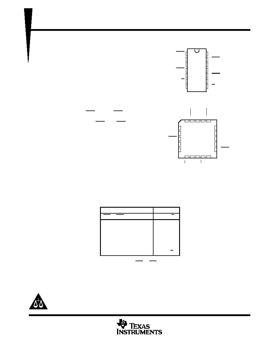
1CLR
1D
1CLK
1PRE
1Q
1Q
GND
V
CC
2CLR
2D
2CLK
2PRE
2Q
2Q
3
2
1 20 19
9 10 11 12 13
4
5
6
7
8
18
17
16
15
14
2D
NC
2CLK
NC
2PRE
1CLK
NC
1PRE
NC
1Q
SN54ACT74 . . . FK PACKAGE
(TOP VIEW)
1D
1CLR
NC
2Q
2Q
V
2CLR
1Q
GND
NC
CC
SN54ACT74 . . . J OR W PACKAGE
SN74ACT74 . . . D, DB, N, OR PW PACKAGE
(TOP VIEW)
NC ¡ No internal connection
On products compliant to MIL-PRF-38535, all parameters are tested
unless otherwise noted. On all other products, production
processing does not necessarily include testing of all parameters.
SN54ACT74, SN74ACT74
DUAL POSITIVE-EDGE-TRIGGERED D-TYPE FLIP-FLOPS
WITH CLEAR AND PRESET
SCAS520E ¡ AUGUST 1995 ¡ REVISED JANUARY 2000
2
POST OFFICE BOX 655303
À
DALLAS, TEXAS 75265
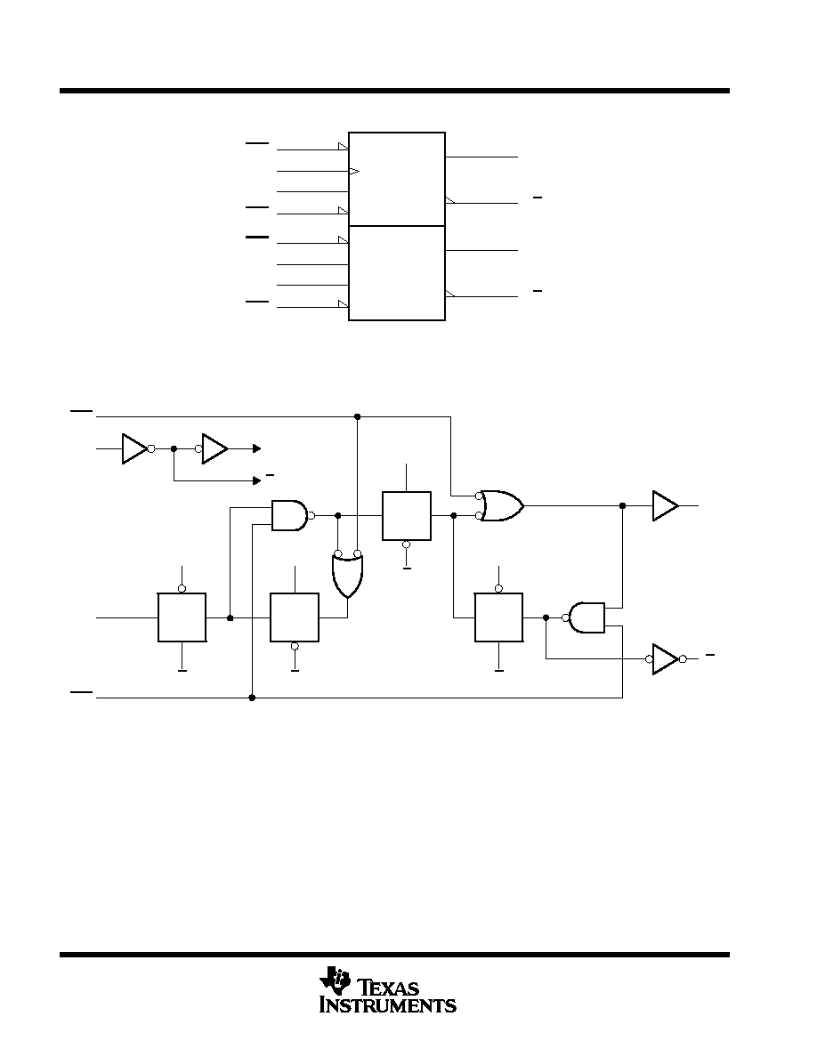
logic symbol
S
4
3
1CLK
1D
2
1D
R
1
1Q
5
6
C1
10
11
2CLK
12
2D
13
2Q
9
8
1PRE
2PRE
1CLR
2CLR
1Q
2Q
This symbol is in accordance with ANSI/IEEE Std 91-1984 and IEC Publication 617-12.
Pin numbers shown are for the D, DB, J, N, PW, and W packages.
logic diagram, each flip-flop (positive logic)
C
C
C
C
C
C
C
C
TG
TG
TG
TG
Q
Q
PRE
CLK
D
CLR
C
C
SN54ACT74, SN74ACT74
DUAL POSITIVE-EDGE-TRIGGERED D-TYPE FLIP-FLOPS
WITH CLEAR AND PRESET
SCAS520E ¡ AUGUST 1995 ¡ REVISED JANUARY 2000
3
POST OFFICE BOX 655303
À
DALLAS, TEXAS 75265
absolute maximum ratings over operating free-air temperature range (unless otherwise noted)
Supply voltage range, V
CC
¡0.5 V to 7 V
. . . . . . . . . . . . . . . . . . . . . . . . . . . . . . . . . . . . . . . . . . . . . . . . . . . . . . . . . .
Input voltage range, V
I
(see Note 1)
¡0.5 V to V
CC
+ 0.5 V
. . . . . . . . . . . . . . . . . . . . . . . . . . . . . . . . . . . . . . . . . . .
Output voltage range, V
O
(see Note 1)
¡0.5 V to V
CC
+ 0.5 V
. . . . . . . . . . . . . . . . . . . . . . . . . . . . . . . . . . . . . . . .
Input clamp current, I
IK
(V
I
< 0 or V
I
> V
CC
)
▒
20 mA
. . . . . . . . . . . . . . . . . . . . . . . . . . . . . . . . . . . . . . . . . . . . . . . .
Output clamp current, I
OK
(V
O
< 0 or V
O
> V
CC
)
▒
20 mA
. . . . . . . . . . . . . . . . . . . . . . . . . . . . . . . . . . . . . . . . . . . .
Continuous output current, I
O
(V
O
= 0 to V
CC
)
▒
50 mA
. . . . . . . . . . . . . . . . . . . . . . . . . . . . . . . . . . . . . . . . . . . . . .
Continuous current through V
CC
or GND
▒
200 mA
. . . . . . . . . . . . . . . . . . . . . . . . . . . . . . . . . . . . . . . . . . . . . . . . . .
Package thermal impedance,
JA
(see Note 2): D package
86
░
C/W
. . . . . . . . . . . . . . . . . . . . . . . . . . . . . . . . . . .
DB package
96
░
C/W
. . . . . . . . . . . . . . . . . . . . . . . . . . . . . . . . .
N package
80
░
C/W
. . . . . . . . . . . . . . . . . . . . . . . . . . . . . . . . . . .
PW package
113
░
C/W
. . . . . . . . . . . . . . . . . . . . . . . . . . . . . . . .
Storage temperature range, T
stg
¡65
░
C to 150
░
C
. . . . . . . . . . . . . . . . . . . . . . . . . . . . . . . . . . . . . . . . . . . . . . . . . . .
Stresses beyond those listed under "absolute maximum ratings" may cause permanent damage to the device. These are stress ratings only, and
functional operation of the device at these or any other conditions beyond those indicated under "recommended operating conditions" is not
implied. Exposure to absolute-maximum-rated conditions for extended periods may affect device reliability.
NOTES:
1. The input and output voltage ratings may be exceeded if the input and output current ratings are observed.
2. The package thermal impedance is calculated in accordance with JESD 51.
recommended operating conditions (see Note 3)
SN54ACT74
SN74ACT74
UNIT
MIN
MAX
MIN
MAX
UNIT
VCC
Supply voltage
4.5
5.5
4.5
5.5
V
VIH
High-level input voltage
2
2
V
VIL
Low-level input voltage
0.8
0.8
V
VI
Input voltage
0
VCC
0
VCC
V
VO
Output voltage
0
VCC
0
VCC
V
IOH
High-level output current
¡24
¡24
mA
IOL
Low-level output current
24
24
mA
t/
v
Input transition rise or fall rate
0
8
0
8
ns/V
TA
Operating free-air temperature
¡55
125
¡40
85
░
C
NOTE 3: All unused inputs of the device must be held at VCC or GND to ensure proper device operation. Refer to the TI application report
Implications of Slow or Floating CMOS Inputs, literature number SCBA004.

SN54ACT74, SN74ACT74
DUAL POSITIVE-EDGE-TRIGGERED D-TYPE FLIP-FLOPS
WITH CLEAR AND PRESET
SCAS520E ¡ AUGUST 1995 ¡ REVISED JANUARY 2000
4
POST OFFICE BOX 655303
À
DALLAS, TEXAS 75265
electrical characteristics over recommended operating free-air temperature range (unless
otherwise noted)
PARAMETER
TEST CONDITIONS
V
TA = 25
░
C
SN54ACT74
SN74ACT74
UNIT
PARAMETER
TEST CONDITIONS
VCC
MIN
TYP
MAX
MIN
MAX
MIN
MAX
UNIT
IOH = 50
Á
A
4.5 V
4.4
4.49
4.4
4.4
IOH = ¡50
Á
A
5.5 V
5.4
5.49
5.4
5.4
VOH
IOH = 24 mA
4.5 V
3.86
3.7
3.76
V
VOH
IOH = ¡24 mA
5.5 V
4.86
4.7
4.76
V
IOH = ¡50 mA
5.5 V
3.86
IOH = ¡75 mA
5.5 V
3.85
IOL = 50
Á
A
4.5 V
0.001
0.1
0.1
0.1
IOL = 50
Á
A
5.5 V
0.001
0.1
0.1
0.1
VOL
IOL = 24 mA
4.5 V
0.36
0.5
0.44
V
VOL
IOL = 24 mA
5.5 V
0.36
0.5
0.44
V
IOL = 50 mA
5.5 V
1.65
IOL = 75 mA
5.5 V
1.65
II
VI = VCC or GND
5.5 V
▒
0.1
▒
1
▒
1
Á
A
ICC
VI = VCC or GND,
IO = 0
5.5 V
2
40
20
Á
A
ICC
One input at 3.4 V,
Other inputs at GND or VCC
5.5 V
0.6
1.6
1.5
mA
Ci
VI = VCC or GND
5 V
3
pF
Not more than one output should be tested at a time, and the duration of the test should not exceed 2 ms.
This is the increase in supply current for each input that is at one of the specified TTL voltage levels rather than 0 V or VCC.
timing characteristics over recommended ranges of supply voltage and operating free-air
temperature (unless otherwise noted) (see Figure 1)
TA = 25
░
C
SN54ACT74
SN74ACT74
UNIT
MIN
MAX
MIN
MAX
MIN
MAX
UNIT
fclock
Clock frequency
0
145
0
145
0
145
MHz
t
Pulse duration
PRE or CLR low
5
7
6
ns
tw
Pulse duration
CLK
5
7
6
ns
t
Set p time data before CLK
Data
3
4
3.5
ns
tsu
Setup time, data before CLK
PRE or CLR inactive
0
0.5
0
ns
th
Hold time, data after CLK
1
1
1
ns
switching characteristics over recommended operating free-air temperature (unless otherwise
noted) (see Figure 1)
FROM
TO
SN54ACT74
PARAMETER
FROM
(INPUT)
TO
(OUTPUT)
TA = 25
░
C
MIN
MAX
UNIT
(INPUT)
(OUTPUT)
MIN
TYP
MAX
MIN
MAX
fmax
145
210
85
MHz
tPLH
PRE or CLR
Q or Q
1
5.5
9.5
1
11.5
ns
tPHL
PRE or CLR
Q or Q
1
6
10
1
12.5
ns
tPLH
CLK
Q or Q
1
7.5
11
1
14
ns
tPHL
CLK
Q or Q
1
6
10
1
12
ns
SN54ACT74, SN74ACT74
DUAL POSITIVE-EDGE-TRIGGERED D-TYPE FLIP-FLOPS
WITH CLEAR AND PRESET
SCAS520E ¡ AUGUST 1995 ¡ REVISED JANUARY 2000
5
POST OFFICE BOX 655303
À
DALLAS, TEXAS 75265
switching characteristics over recommended operating free-air temperature (unless otherwise
noted) (see Figure 1)
FROM
TO
SN74ACT74
PARAMETER
FROM
(INPUT)
TO
(OUTPUT)
TA = 25
░
C
MIN
MAX
UNIT
(INPUT)
(OUTPUT)
MIN
TYP
MAX
MIN
MAX
fmax
145
210
125
MHz
tPLH
PRE or CLR
Q or Q
3
5.5
9.5
2.5
10.5
ns
tPHL
PRE or CLR
Q or Q
3
6
10
3
11.5
ns
tPLH
CLK
Q or Q
4
7.5
11
4
13
ns
tPHL
CLK
Q or Q
3.5
6
10
3
11.5
ns
operating characteristics, V
CC
= 5 V, T
A
= 25
░
C
PARAMETER
TEST CONDITIONS
TYP
UNIT
Cpd
Power dissipation capacitance
CL = 50 pF,
f = 1 MHz
45
pF
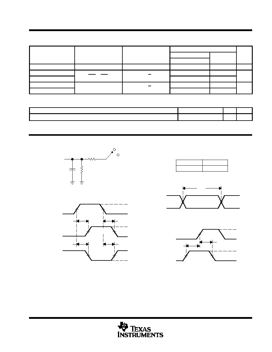
PARAMETER MEASUREMENT INFORMATION
50% VCC
3 V
3 V
0 V
0 V
th
tsu
VOLTAGE WAVEFORMS
Data Input
tPLH
tPHL
tPHL
tPLH
VOH
VOH
VOL
VOL
3 V
0 V
50% VCC
50% VCC
Input
Out-of-Phase
Output
In-Phase
Output
Timing Input
50% VCC
VOLTAGE WAVEFORMS
tPLH/tPHL
Open
TEST
S1
3 V
0 V
tw
VOLTAGE WAVEFORMS
Input
NOTES: A. CL includes probe and jig capacitance.
B. All input pulses are supplied by generators having the following characteristics: PRR
1 MHz, ZO = 50
, tr
2.5 ns, tf
2.5 ns.
C. The outputs are measured one at a time with one input transition per measurement.
LOAD CIRCUIT
From Output
Under Test
CL = 50 pF
(see Note A)
S1
2
Î
VCC
500
500
Open
1.5 V
1.5 V
1.5 V
1.5 V
1.5 V
1.5 V
1.5 V
Figure 1. Load Circuit and Voltage Waveforms