SN74ACT16245Q-EP
16-BIT BUS TRANSCEIVER
WITH 3-STATE OUTPUTS
SCAS677A ş MAY 2002 ş REVISED JULY 2002
1
POST OFFICE BOX 655303
Ě
DALLAS, TEXAS 75265
D
Controlled Baseline
ş One Assembly/Test Site, One Fabrication
Site
D
Extended Temperature Performance of
ş40
░
C to 125
░
C
D
Enhanced Diminishing Manufacturing
Sources (DMS) Support
D
Enhanced Product Change Notification
D
Qualification Pedigree
D
Member of the Texas Instruments
Widebus
Family
D
Inputs Are TTL-Voltage Compatible
D
3-State Outputs Drive Bus Lines Directly
D
Flow-Through Architecture Optimizes PCB
Layout
D
Distributed V
CC
and GND Pins Minimize
High-Speed Switching Noise
Component qualification in accordance with JEDEC and industry
standards to ensure reliable operation over an extended
temperature range. This includes, but is not limited to, highly
accelerated stress test (HAST) or biased 85/85, temperature
cycle, autoclave or unbiased HAST, electromigration, bond
intermetallic life, and mold compound life.
description
The SN74ACT16245Q-EP is a 16-bit bus
transceiver organized as dual-octal noninverting
3-state transceivers and designed for
asynchronous two-way communication between
data buses. The control-function implementation
minimizes external timing requirements.
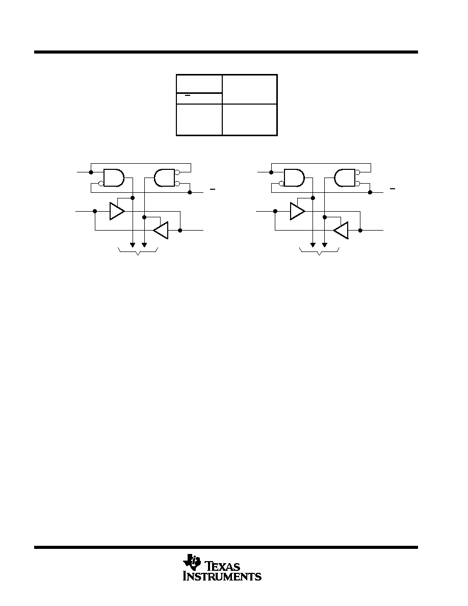
The device allows data transmission from the A bus to the B bus or from the B bus to the A bus, depending on
the logic level at the direction-control (DIR) input. The enable (G) input can be used to disable the devices so
that the buses are effectively isolated.
ORDERING INFORMATION
TA
PACKAGE
ORDERABLE
PART NUMBER
TOP-SIDE
MARKING
ş40
░
C to 125
░
C
SSOP ş DL
Tape and reel
SN74ACT16245QDLREP
ACT16245QEP
Package drawings, standard packing quantities, thermal data, symbolization, and PCB design guidelines are
available at www.ti.com/sc/package.
Copyright
2002, Texas Instruments Incorporated
PRODUCTION DATA information is current as of publication date.
Products conform to specifications per the terms of Texas Instruments
standard warranty. Production processing does not necessarily include
testing of all parameters.
Please be aware that an important notice concerning availability, standard warranty, and use in critical applications of
Texas Instruments semiconductor products and disclaimers thereto appears at the end of this data sheet.
Widebus is a trademark of Texas Instruments.
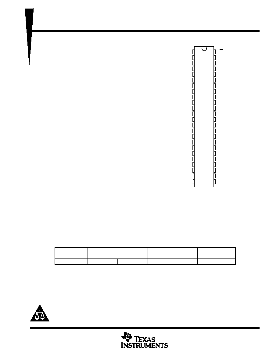
DL PACKAGE
(TOP VIEW)
1
2
3
4
5
6
7
8
9
10
11
12
13
14
15
16
17
18
19
20
21
22
23
24
48
47
46
45
44
43
42
41
40
39
38
37
36
35
34
33
32
31
30
29
28
27
26
25
1DIR
1B1
1B2
GND
1B3
1B4
V
CC
1B5
1B6
GND
1B7
1B8
2B1
2B2
GND
2B3
2B4
V
CC
2B5
2B6
GND
2B7
2B8
2DIR
1G
1A1
1A2
GND
1A3
1A4
V
CC
1A5
1A6
GND
1A7
1A8
2A1
2A2
GND
2A3
2A4
V
CC
2A5
2A6
GND
2A7
2A8
2G
SN74ACT16245Q-EP
16-BIT BUS TRANSCEIVER
WITH 3-STATE OUTPUTS
SCAS677A ş MAY 2002 ş REVISED JULY 2002
2
POST OFFICE BOX 655303
Ě
DALLAS, TEXAS 75265
FUNCTION TABLE
(each section)
CONTROL
INPUTS
OPERATION
G
DIR
L
L
B data to A bus
L
H
A data to B bus
H
X
Isolation
logic diagram (positive logic)
1DIR
1A1
1G
1B1
To Seven Other Transceivers
2DIR
2A1
2G
2B1
To Seven Other Transceivers
1
47
24
36
48
2
25
13
absolute maximum ratings over operating free-air temperature range (unless otherwise noted)
Supply voltage range, V
CC
ş0.5 V to 7 V
. . . . . . . . . . . . . . . . . . . . . . . . . . . . . . . . . . . . . . . . . . . . . . . . . . . . . . . . . .
Input voltage range, V
I
(see Note 1)
ş0.5 V to V
CC
+ 0.5 V
. . . . . . . . . . . . . . . . . . . . . . . . . . . . . . . . . . . . . . . . . . . .
Output voltage range, V
O
(see Note 1)
ş0.5 V to V
CC
+ 0.5 V
. . . . . . . . . . . . . . . . . . . . . . . . . . . . . . . . . . . . . . . . .
Input clamp current, I
IK
(V
I
< 0 or V
I
> V
CC
)
▒
20 mA
. . . . . . . . . . . . . . . . . . . . . . . . . . . . . . . . . . . . . . . . . . . . . . . . .
Output clamp current, I
OK
(V
O
< 0 or V
O
> V
CC
)
▒
24 mA
. . . . . . . . . . . . . . . . . . . . . . . . . . . . . . . . . . . . . . . . . . . .
Continuous output current, I
O
(V
O
= 0 to V
CC
)
▒
24 mA
. . . . . . . . . . . . . . . . . . . . . . . . . . . . . . . . . . . . . . . . . . . . . .
Continuous current through V
CC
or GND
▒
260 mA
. . . . . . . . . . . . . . . . . . . . . . . . . . . . . . . . . . . . . . . . . . . . . . . . . .
Maximum power dissipation at T
A
= 55
░
C (in still air) (see Note 2): DL package
1.2 W
. . . . . . . . . . . . . . . . . . .
Storage temperature range, T
stg
ş65
░
C to 150
░
C
. . . . . . . . . . . . . . . . . . . . . . . . . . . . . . . . . . . . . . . . . . . . . . . . . . . .
Stresses beyond those listed under "absolute maximum ratings" may cause permanent damage to the device. These are stress ratings only, and
functional operation of the device at these or any other conditions beyond those indicated under "recommended operating conditions" is not
implied. Exposure to absolute-maximum-rated conditions for extended periods may affect device reliability.
NOTES:
1. The input and output voltage ratings may be exceeded if the input and output current ratings are observed.
2. The maximum package power dissipation is calculated using a junction temperature of 150
░
C and a board trace length of 750 mils.
SN74ACT16245Q-EP
16-BIT BUS TRANSCEIVER
WITH 3-STATE OUTPUTS
SCAS677A ş MAY 2002 ş REVISED JULY 2002
3
POST OFFICE BOX 655303
Ě
DALLAS, TEXAS 75265
recommended operating conditions (see Note 3)
MIN
MAX
UNIT
VCC
Supply voltage (see Note 4)
4.5
5.5
V
VIH
High-level input voltage
2
V
VIL
Low-level input voltage
0.8
V
VI
Input voltage
0
VCC
V
VO
Output voltage
0
VCC
V
IOH
High-level output current
ş16
mA
IOL
Low-level output current
16
mA
t/
v
Input transition rise or fall rate
0
10
ns/V
TA
Operating free-air temperature
ş40
125
░
C
NOTES:
3. Unused inputs should be tied to VCC through a pullup resistor of approximately 5 k
W
or greater to keep them from floating. Refer
to the TI application report, Implications of Slow or Floating CMOS Inputs, literature number SCBA004.
4. All VCC and GND pins must be connected to the proper-voltage power supply.
SN74ACT16245Q-EP
16-BIT BUS TRANSCEIVER
WITH 3-STATE OUTPUTS
SCAS677A ş MAY 2002 ş REVISED JULY 2002
4
POST OFFICE BOX 655303
Ě
DALLAS, TEXAS 75265
electrical characteristics over recommended operating free-air temperature range (unless
otherwise noted)
PARAMETER
TEST CONDITIONS
VCC
TA = 25
░
C
MIN
MAX
UNIT
PARAMETER
TEST CONDITIONS
VCC
MIN
TYP
MAX
MIN
MAX
UNIT
IOH = 50
m
A
4.5 V
4.4
4.4
IOH = ş50
m
A
5.5 V
5.4
5.4
VOH
IOH = 16 mA
4.5 V
3.94
3.94
V
IOH = ş16 mA
5.5 V
4.94
4.94
IOH = ş24 mA
{
5.5 V
3.85
IOL = 50
m
A
4.5 V
0.1
0.1
IOL = 50
m
A
5.5 V
0.1
0.1
VOL
IOL = 16 mA
4.5 V
0.36
0.5
V
IOL = 16 mA
5.5 V
0.36
0.5
IOL = 24 mA
{
5.5 V
0.5
II
Control inputs
VI = VCC or GND
5.5 V
▒
0.1
▒
1
m
A
IOZ
A or B ports
}
VO = VCC or GND
5.5 V
▒
0.5
▒
10
m
A
ICC
VI = VCC or GND,
IO = 0
5.5 V
8
160
m
A
ICC
w
One input at 3.4 V,
Other inputs at GND or VCC
5.5 V
0.9
1
mA
Ci
Control inputs
VI = VCC or GND
5 V
4.5
pF
Cio
A or B ports
VO = VCC or GND
5 V
16
pF
Not more than one output should be tested at a time, and the duration of the test should not exceed 10 ms.
For I/O ports, the parameter IOZ includes the input leakage current II.
ž This is the increase in supply current for each input that is at one of the specified TTL-voltage levels rather than 0 V or VCC.
switching characteristics over recommended ranges of supply voltage and operating free-air
temperature (unless otherwise noted) (see Figure 1)
PARAMETER
FROM
TO
TA = 25
░
C
MIN
MAX
UNIT
PARAMETER
(INPUT)
(OUTPUT)
MIN
TYP
MAX
MIN
MAX
UNIT
tPLH
A or B
B or A
3.2
6.9
9.3
3.2
11.5
ns
tPHL
A or B
B or A
2.6
6.4
9.2
2.6
11.1
ns
tPZH
G
B or A
2.7
6.4
9.1
2.7
10.9
ns
tPZL
G
B or A
3.4
7.4
10.5
3.4
12.6
ns
tPHZ
G
B or A
5.8
9.2
11.6
5.8
13.4
ns
tPLZ
G
B or A
5.5
8.5
10.8
5.5
12.7
ns
operating characteristics, V
CC
= 5 V, T
A
= 25
░
C
PARAMETER
TEST CONDITIONS
TYP
UNIT
C d
Power dissipation capacitance per transceiver
Outputs enabled
CL = 50 pF
f = 1 MHz
52
pF
Cpd
Power dissipation capacitance per transceiver
Outputs disabled
CL = 50 pF,
f = 1 MHz
10
pF
SN74ACT16245Q-EP
16-BIT BUS TRANSCEIVER
WITH 3-STATE OUTPUTS
SCAS677A ş MAY 2002 ş REVISED JULY 2002
5
POST OFFICE BOX 655303
Ě
DALLAS, TEXAS 75265
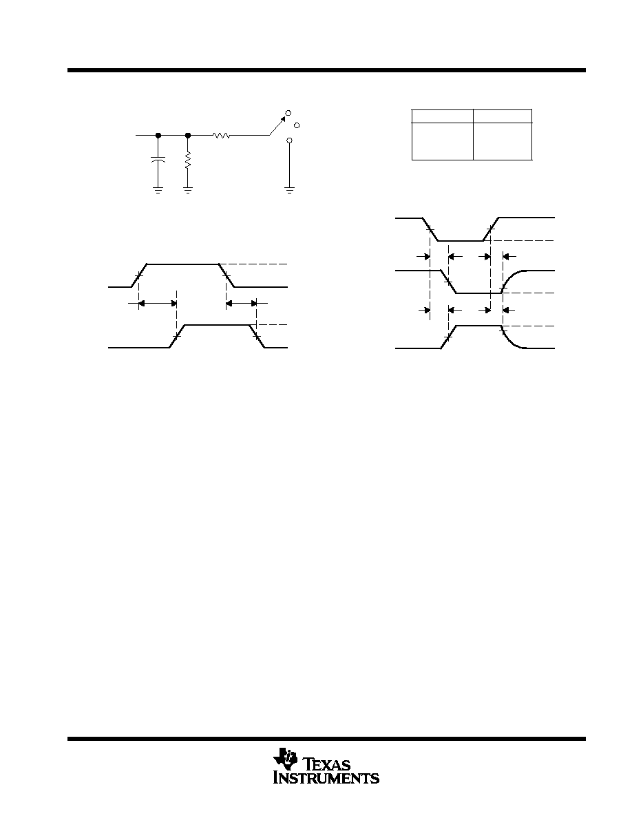
PARAMETER MEASUREMENT INFORMATION
From Output
Under Test
CL = 50 pF
(see Note A)
LOAD CIRCUIT
S1
2
Î
VCC
500
500
tPLH
tPHL
Output
Control
(low-level
enabling)
Output
Waveform 1
S1 at 2
Î
VCC
(see Note B)
Output
Waveform 2
S1 at GND
(see Note B)
VOL
VOH
tPZL
tPZH
tPLZ
tPHZ
1.5 V
1.5 V
1.5 V
1.5 V
VCC
3 V
0 V
50% VCC
50% VCC
VOH
VOL
0 V
50% VCC
20% VCC
50% VCC
80% VCC
0 V
3 V
GND
Open
Input
Output
VOLTAGE WAVEFORMS
VOLTAGE WAVEFORMS
tPLH/tPHL
tPLZ/tPZL
tPHZ/tPZH
Open
2
Î
VCC
GND
TEST
S1
NOTES: A. CL includes probe and jig capacitance.
B. Waveform 1 is for an output with internal conditions such that the output is low except when disabled by the output control.
Waveform 2 is for an output with internal conditions such that the output is high except when disabled by the output control.
C. All input pulses are supplied by generators having the following characteristics: PRR
1 MHz, ZO = 50
, tr = 3 ns, tf = 3 ns.
D. The outputs are measured one at a time with one input transition per measurement.
Figure 1. Load Circuit and Voltage Waveforms