SN54ABTH162245, SN74ABTH162245
16-BIT BUS TRANSCEIVERS
WITH 3-STATE OUTPUTS
SCBS712A FEBRUARY 1998 REVISED APRIL 1999
1
POST OFFICE BOX 655303
·
DALLAS, TEXAS 75265
D
Members of the Texas Instruments
Widebus
TM
Family
D
A-Port Outputs Have Equivalent 25-
Series Resistors, So No External Resistors
Are Required
D
State-of-the-Art
EPIC-
B
TM
BiCMOS Design
Significantly Reduces Power Dissipation
D
Typical V
OLP
(Output Ground Bounce)
< 1 V at V
CC
= 5 V, T
A
= 25
°
C
D
Distributed V
CC
and GND Pin Configuration
Minimizes High-Speed Switching Noise
D
Flow-Through Architecture Optimizes PCB
Layout
D
Bus Hold on Data Inputs Eliminates the
Need for External Pullup/Pulldown
Resistors
D
Latch-Up Performance Exceeds 500 mA Per
JESD 17
D
ESD Protection Exceeds 2000 V Per
MIL-STD-833, Method 3015; Exceeds 200 V
Using Machine Model (C = 200 pF, R = 0)
D
Package Options Include Plastic Thin
Shrink Small-Outline (DGG), Thin Very
Small-Outline (DGV), and Shrink
Small-Outline (DL) Packages and 380-mil
Fine-Pitch Ceramic Flat (WD) Package
Using 25-mil Center-to-Center Spacings
description
The 'ABTH162245 devices are 16-bit noninverting 3-state transceivers designed for synchronous two-way
communication between data buses. The control-function implementation minimizes external timing
requirements.
These devices can be used as two 8-bit transceivers or one 16-bit transceiver. They allow data transmission
from the A bus to the B bus or from the B bus to the A bus, depending on the logic level at the direction-control
(DIR) input. The output-enable (OE) input can be used to disable the device so that the buses are effectively
isolated.
The A-port outputs, which are designed to source or sink up to 12 mA, include equivalent 25-
series resistors
to reduce overshoot and undershoot.
Active bus-hold circuitry is provided to hold unused or floating data inputs at a valid logic level.
To ensure the high-impedance state during power up or power down, OE should be tied to V
CC
through a pullup
resistor; the minimum value of the resistor is determined by the current-sinking capability of the driver.
The SN54ABTH162245 is characterized for operation over the full military temperature range of 55
°
C to
125
°
C. The SN74ABTH162245 is characterized for operation from 40
°
C to 85
°
C.
Copyright
©
1999, Texas Instruments Incorporated
UNLESS OTHERWISE NOTED this document contains PRODUCTION
DATA information current as of publication date. Products conform to
specifications per the terms of Texas Instruments standard warranty.
Production processing does not necessarily include testing of all
parameters.
Please be aware that an important notice concerning availability, standard warranty, and use in critical applications of
Texas Instruments semiconductor products and disclaimers thereto appears at the end of this data sheet.
Widebus and EPIC-
B are trademarks of Texas Instruments Incorporated.
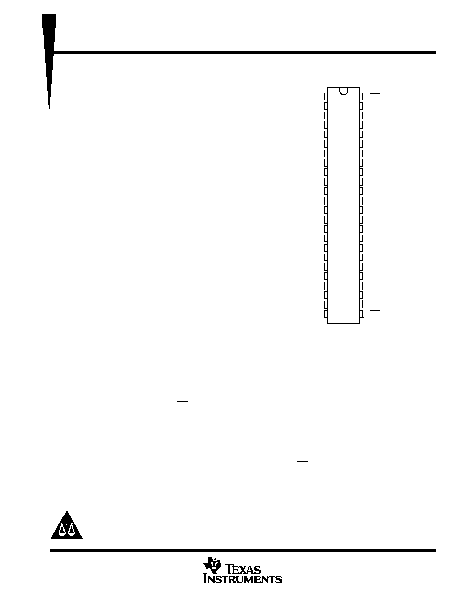
SN54ABTH162245 . . . WD PACKAGE
SN74ABTH162245 . . . DGG, DGV, OR DL PACKAGE
(TOP VIEW)
1
2
3
4
5
6
7
8
9
10
11
12
13
14
15
16
17
18
19
20
21
22
23
24
48
47
46
45
44
43
42
41
40
39
38
37
36
35
34
33
32
31
30
29
28
27
26
25
1DIR
1B1
1B2
GND
1B3
1B4
V
CC
1B5
1B6
GND
1B7
1B8
2B1
2B2
GND
2B3
2B4
V
CC
2B5
2B6
GND
2B7
2B8
2DIR
1OE
1A1
1A2
GND
1A3
1A4
V
CC
1A5
1A6
GND
1A7
1A8
2A1
2A2
GND
2A3
2A4
V
CC
2A5
2A6
GND
2A7
2A8
2OE
SN54ABTH162245, SN74ABTH162245
16-BIT BUS TRANSCEIVERS
WITH 3-STATE OUTPUTS
SCBS712A FEBRUARY 1998 REVISED APRIL 1999
2
POST OFFICE BOX 655303
·
DALLAS, TEXAS 75265
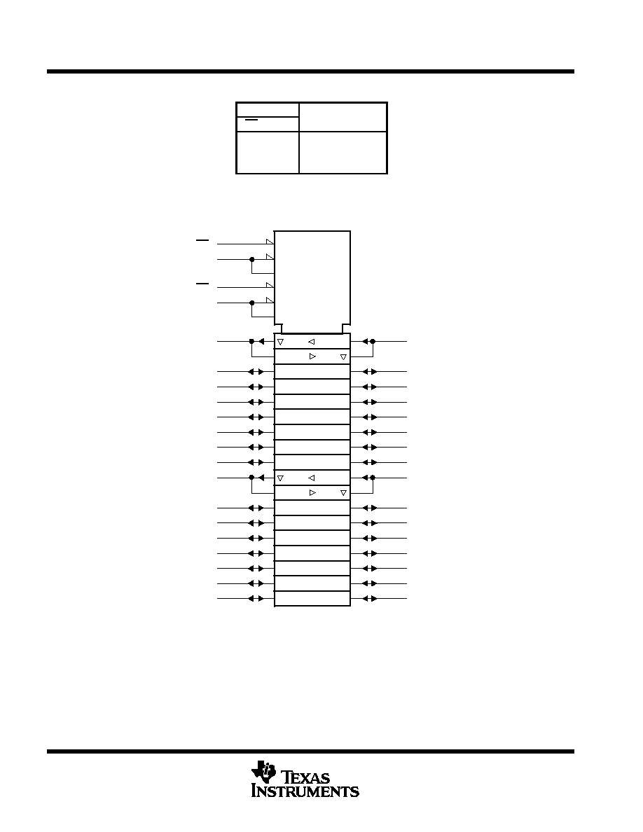
FUNCTION TABLE
(each 8-bit section)
INPUTS
OPERATION
OE
DIR
OPERATION
L
L
B data to A bus
L
H
A data to B bus
H
X
Isolation
logic symbol
1A2
46
1A3
44
1A4
43
1A5
41
1A6
40
1A7
38
1A8
37
2A2
35
2A3
33
2A4
32
2A5
30
2A6
29
2A7
27
2A8
26
1OE
2OE
This symbol is in accordance with ANSI/IEEE Std 91-1984 and IEC Publication 617-12.
1A1
47
G3
48
3 EN1 [BA]
1
1DIR
3 EN2 [AB]
G6
25
6 EN4 [BA]
24
2DIR
6 EN5 [AB]
1B1
2
1B2
3
1B3
5
1B4
6
1B5
8
1B6
9
1B7
11
1B8
12
2A1
36
2B1
13
2B2
14
2B3
16
2B4
17
2B5
19
2B6
20
2B7
22
2B8
23
1
2
4
5
SN54ABTH162245, SN74ABTH162245
16-BIT BUS TRANSCEIVERS
WITH 3-STATE OUTPUTS
SCBS712A FEBRUARY 1998 REVISED APRIL 1999
3
POST OFFICE BOX 655303
·
DALLAS, TEXAS 75265
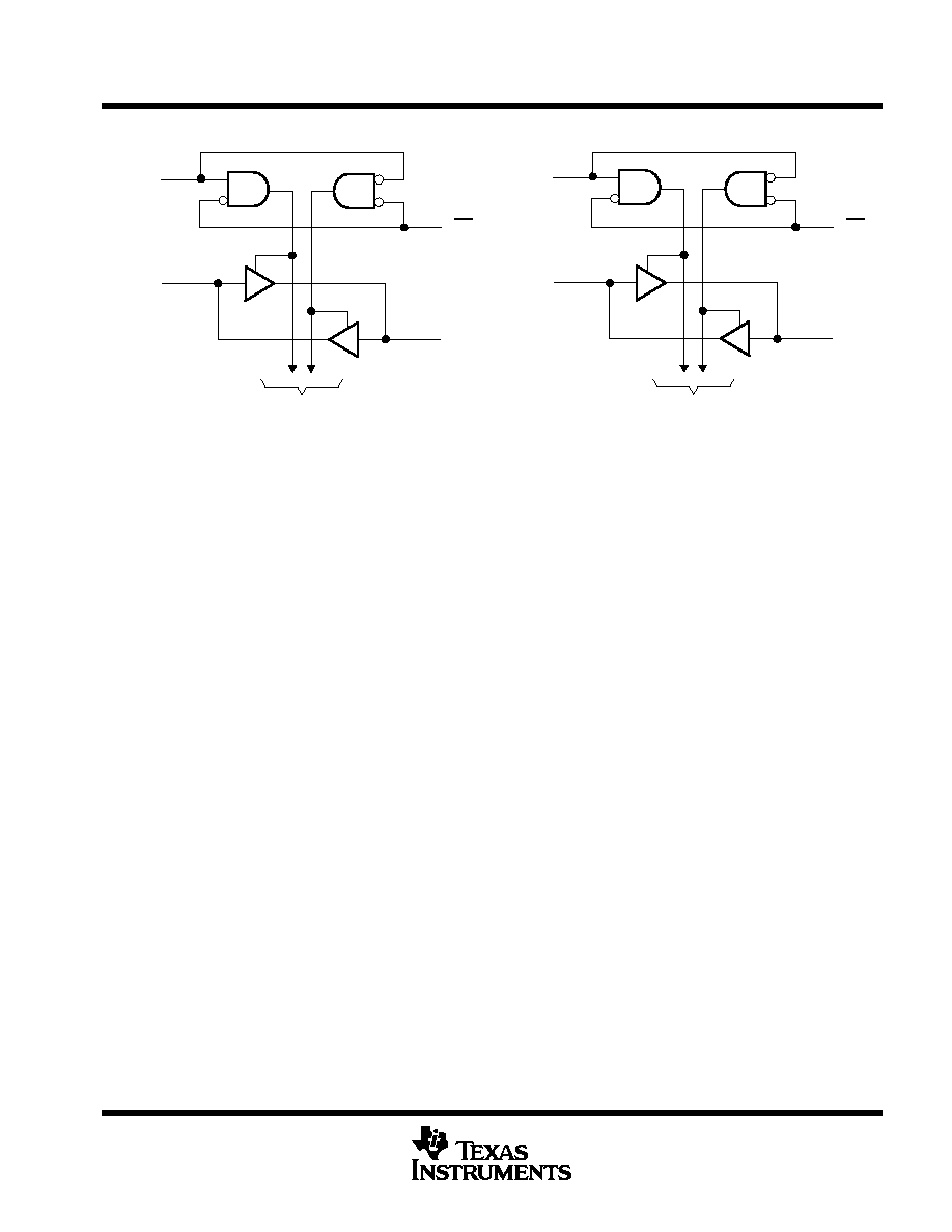
logic diagram (positive logic)
To Seven Other Channels
1DIR
1A1
1B1
1OE
To Seven Other Channels
2DIR
2A1
2B1
2OE
1
47
24
36
48
2
25
13
absolute maximum ratings over operating free-air temperature range (unless otherwise noted)
Supply voltage range, V
CC
0.5 V to 7 V
. . . . . . . . . . . . . . . . . . . . . . . . . . . . . . . . . . . . . . . . . . . . . . . . . . . . . . . . . .
Input voltage range, V
I
(except I/O ports) (see Note 1)
0.5 V to 7 V
. . . . . . . . . . . . . . . . . . . . . . . . . . . . . . . . . .
Voltage range applied to any output in the high or power-off state, V
O
0.5 V to 5.5 V
. . . . . . . . . . . . . . . . . . .
Current into any output in the low state, I
O
: SN54ABTH162245 (B port)
96 mA
. . . . . . . . . . . . . . . . . . . . . . . .
SN74ABTH162245 (B port)
128 mA
. . . . . . . . . . . . . . . . . . . . . . .
SN54/74ABTH162245 (A port)
30 mA
. . . . . . . . . . . . . . . . . . . . . .
Input clamp current, I
IK
(V
I
< 0)
18 mA
. . . . . . . . . . . . . . . . . . . . . . . . . . . . . . . . . . . . . . . . . . . . . . . . . . . . . . . . . . .
Output clamp current, I
OK
(V
O
< 0)
50 mA
. . . . . . . . . . . . . . . . . . . . . . . . . . . . . . . . . . . . . . . . . . . . . . . . . . . . . . . .
Package thermal impedance,
JA
(see Note 2): DGG package
89
°
C/W
. . . . . . . . . . . . . . . . . . . . . . . . . . . . . . . .
DGV package
93
°
C/W
. . . . . . . . . . . . . . . . . . . . . . . . . . . . . . . .
DL package
94
°
C/W
. . . . . . . . . . . . . . . . . . . . . . . . . . . . . . . . . .
Storage temperature range, T
stg
65
°
C to 150
°
C
. . . . . . . . . . . . . . . . . . . . . . . . . . . . . . . . . . . . . . . . . . . . . . . . . . .
Stresses beyond those listed under "absolute maximum ratings" may cause permanent damage to the device. These are stress ratings only, and
functional operation of the device at these or any other conditions beyond those indicated under "recommended operating conditions" is not
implied. Exposure to absolute-maximum-rated conditions for extended periods may affect device reliability.
NOTES:
1. The input and output negative-voltage ratings may be exceeded if the input and output clamp-current ratings are observed.
2. The package thermal impedance is calculated in accordance with JESD 51.
SN54ABTH162245, SN74ABTH162245
16-BIT BUS TRANSCEIVERS
WITH 3-STATE OUTPUTS
SCBS712A FEBRUARY 1998 REVISED APRIL 1999
4
POST OFFICE BOX 655303
·
DALLAS, TEXAS 75265
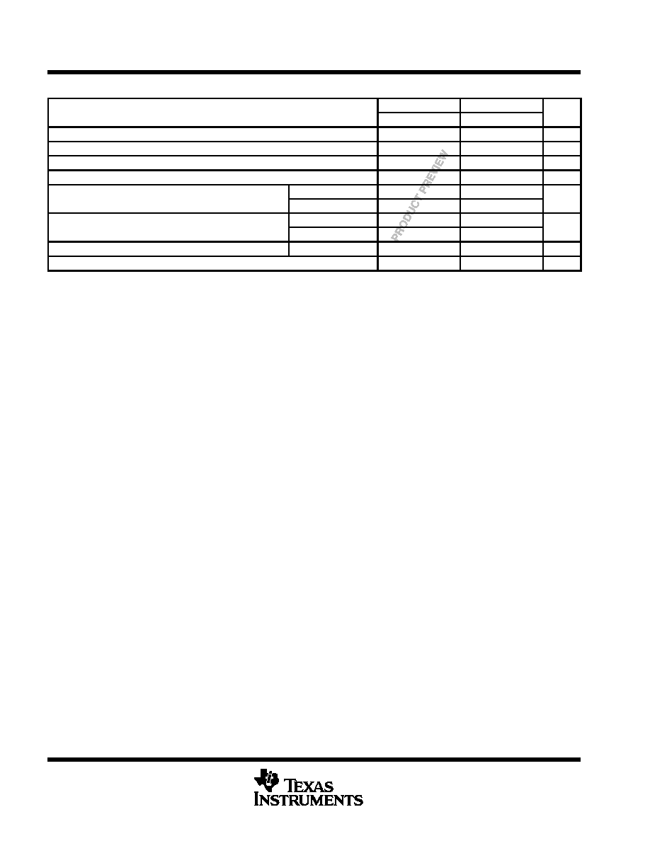
recommended operating conditions (see Note 3)
SN54ABTH162245
SN74ABTH162245
UNIT
MIN
MAX
MIN
MAX
UNIT
VCC
Supply voltage
4.5
5.5
4.5
5.5
V
VIH
High-level input voltage
2
2
V
VIL
Low-level input voltage
0.8
0.8
V
VI
Input voltage
0
VCC
0
VCC
V
IOH
High level output current
B port
24
32
mA
IOH
High-level output current
A port
12
12
mA
IOL
Low level output current
B port
48
64
mA
IOL
Low-level output current
A port
12
12
mA
t/
v
Input transition rise or fall rate
Outputs enabled
10
10
ns/V
TA
Operating free-air temperature
55
125
40
85
°
C
NOTE 3: All unused control inputs of the device must be held at VCC or GND to ensure proper device operation. Refer to the TI application report,
Implications of Slow or Floating CMOS Inputs, literature number SCBA004.
PRODUCT PREVIEW information concerns products in the formative or
design phase of development. Characteristic data and other
specifications are design goals. Texas Instruments reserves the right to
change or discontinue these products without notice.

SN54ABTH162245, SN74ABTH162245
16-BIT BUS TRANSCEIVERS
WITH 3-STATE OUTPUTS
SCBS712A FEBRUARY 1998 REVISED APRIL 1999
5
POST OFFICE BOX 655303
·
DALLAS, TEXAS 75265
electrical characteristics over recommended operating free-air temperature range (unless
otherwise noted)
PARAMETER
TEST CONDITIONS
SN54ABTH162245
SN74ABTH162245
UNIT
PARAMETER
TEST CONDITIONS
MIN
TYP
MAX
MIN
TYP
MAX
UNIT
VIK
VCC = 4.5 V,
II = 18 mA
1.2
1.2
V
VCC = 5 V,
IOH = 1 mA
2.5
2.5
A port
IOH = 1 mA
3
3
A port
VCC = 4.5 V
IOH = 3 mA
3
3.1
VOH
IOH = 12 mA
2.6
V
VOH
VCC = 5 V,
IOH = 3 mA
3
3
V
B port
IOH = 3 mA
2.5
2.5
B port
VCC = 4.5 V
IOH = 24 mA
2
IOH = 32 mA
2
A port
IOL = 12 mA
0.8
0.8
VOL
B port
VCC = 4.5 V
IOL = 48 mA
0.45
0.45
V
B port
IOL = 64 mA
0.55
Vhys
100
100
mV
II
Control
inputs
VCC = 5.5 V, VI = VCC or GND
±
1
±
1
µ
A
I
A or B ports
CC
,
I
CC
±
20
±
20
µ
II(h ld)
VCC = 4 5 V
VI = 0.8 V
100
100
µ
A
II(hold)
VCC = 4.5 V
VI = 2 V
100
100
µ
A
Ioff
VCC = 0,
VI or VO = 0 to 4.5 V
±
100
µ
A
IO
A port
VCC = 5 5 V
VO = 2 5 V
25
90
25
100
mA
IO
B port
VCC = 5.5 V,
VO = 2.5 V
50
180
50
180
mA
ICEX
VCC = 5.5 V,
VO = 5.5 V
Outputs high
50
50
µ
A
VCC = 5.5 V,
Outputs high
2
2
ICC
A or B ports
VCC = 5.5 V,
IO = 0,
Outputs low
32
32
mA
VI = VCC or GND
Outputs disabled
2
2
ICC§
Data inputs
VCC = 5.5 V,
One input at 3.4 V,
Other inputs at VCC or GND
2
2
mA
ICC§
Control
inputs
VCC = 5.5 V, One input at 3.4 V,
Other inputs at VCC or GND
1.5
1.5
Ci
VI = 2.5 V or 0.5 V
3
3
pF
Cio
VO = 2.5 V or 0.5 V
6
6
pF
All typical values are at VCC = 5 V.
Not more than one output should be tested at a time, and the duration of the test should not exceed one second.
§ This is the increase in supply current for each input that is at the specified TTL voltage level rather than VCC or GND.
PRODUCT PREVIEW information concerns products in the formative or
design phase of development. Characteristic data and other
specifications are design goals. Texas Instruments reserves the right to
change or discontinue these products without notice.