
PCM1802
SLES023B Ł DECEMBER 2001 Ł REVISED MARCH 2002
SINGLE-ENDED ANALOG-INPUT
24-BIT, 96-kHz STEREO A/D CONVERTER
1
www.ti.com
FEATURES
D
24-Bit Delta-Sigma Stereo A/D Converter
D
Single-Ended Voltage Input: 3 V p-p
D
Antialiasing Filter Included
D
Oversampling Decimation Filter
Ł Oversampling Frequency:
ū
64,
ū
128
Ł Passband Ripple:
▒
0.05 dB
Ł Stopband Attenuation: Ł65 dB
Ł On-Chip HPF (Low Cut Filter): 0.84 Hz
(44.1 kHz)
D
High Performance
Ł THD+N: 96 dB (Typical)
Ł SNR: 105 dB (Typical)
Ł Dynamic Range: 105 dB (Typical)
D
PCM Audio Interface
Ł Master/Slave Mode Selectable
Ł Data Formats: 24-Bit Left-Justified;
24-Bit I
2
S; 20-, 24-Bit Right-Justified
D
Sampling Rate: 16 kHz to 96 kHz
D
System Clock: 256 f
S
, 384 f
S
, 512 f
S
, 768 f
S
D
Dual Power Supplies: 5 V for Analog, 3.3 V for
Digital
D
Package: 20-Pin SSOP
D
Lead-Free Product
APPLICATIONS
D
AV Amp Receiver
D
MD Player
D
CD Recorder
D
Multitrack Receiver
D
Electric Musical Instrument
DESCRIPTION
The PCM1802 is a high-performance, low-cost,
single-chip stereo analog-to-digital converter with
single-ended analog voltage input. The PCM1802 uses
a delta-sigma modulator with 64- or 128-times over-
sampling, and includes a digital decimation filter and
HPF (low cut filter) which removes the dc component of
the input signal. For various applications, the PCM1802
supports master and slave modes and four data formats
in serial interface. The PCM1802 is suitable for a wide
variety of cost-sensitive consumer applications where
good performance, 5-V analog supply, and 3.3-V digital
supply operation is required. The PCM1802 is
fabricated using a highly advanced CMOS process and
is available in the DB 20-pin SSOP package.
This device contains circuits to protect its inputs and outputs against damage due to high static voltages or electrostatic fields. These
circuits have been qualified to protect this device against electrostatic discharges (ESD) of up to 2 kV according to MIL-STD-883C,
Method 3015; however, it is advised that precautions be taken to avoid application of any voltage higher than maximum-rated
voltages to these high-impedance circuits. During storage or handling, the device leads should be shorted together or the device
should be placed in conductive foam. In a circuit, unused inputs should always be connected to an appropriated logic voltage level,
preferably either VCC or ground. Specific guidelines for handling devices of this type are contained in the publication Guidelines for
Handling Electrostatic-Discharge-Sensitive (ESDS) Devices and Assemblies available from Texas Instruments.
PRODUCTION DATA information is current as of publication date.
Products conform to specifications per the terms of Texas Instruments
standard warranty. Production processing does not necessarily include
testing of all parameters.
Audio Precision and System Two are trademarks of Audio Precision.
Other trademarks are the property of their respective owners.
Copyright
2002, Texas Instruments Incorporated
Please be aware that an important notice concerning availability, standard warranty, and use in critical applications of
Texas Instruments semiconductor products and disclaimers thereto appears at the end of this data sheet.
PCM1802
SLES023B Ł DECEMBER 2001 Ł REVISED MARCH 2002
2
www.ti.com
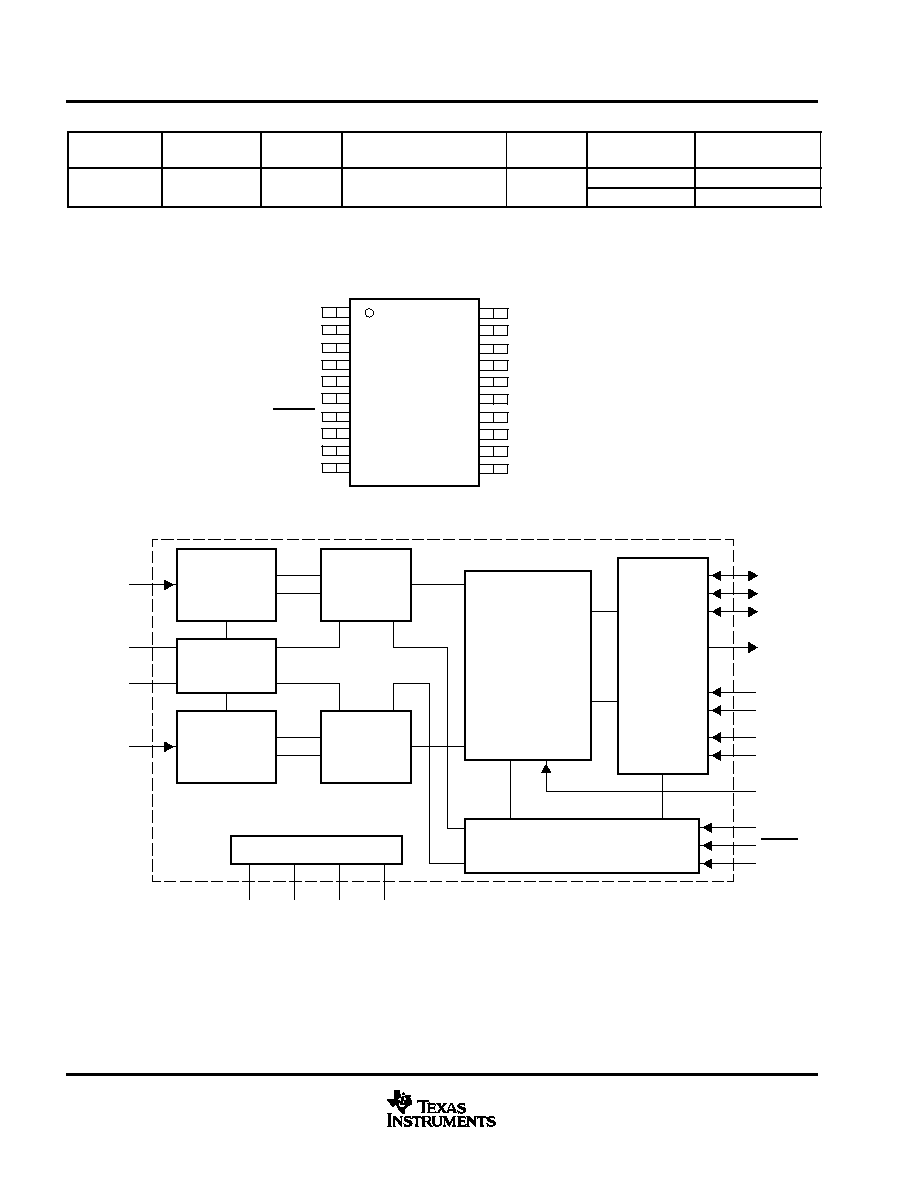
PACKAGE/ORDERING INFORMATION
PRODUCT
PACKAGE
PACKAGE
CODE
OPERATION
TEMPERATURE RANGE
PACKAGE
MARKING
ORDERING
NUMBER
TRANSPORT
MEDIA
PCM1802DB
20 Lead SSOP
20DB
40
░
C to 85
░
C
PCM1802
PCM1802DB
Tube
PCM1802DB
20-Lead SSOP
20DB
Ł40
░
C to 85
░
C
PCM1802
PCM1802DBR
Tape and reel
pin assignments
1
2
3
4
5
6
7
8
9
10
20
19
18
17
16
15
14
13
12
11
V
IN
L
V
IN
R
V
REF
1
V
REF
2
V
CC
AGND
PDWN
BYPAS
FSYNC
LRCK
MODE1
MODE0
FMT1
FMT0
OSR
SCKI
V
DD
DGND
DOUT
BCK
PCM1802
(TOP VIEW)
block diagram
Single-End
/Differential
Converter
BCK
VINL
Reference
Single-End
/Differential
Converter
VREF1
VREF2
VINR
5th Order
Delta-Sigma
Modulator
5th Order
Delta-Sigma
Modulator
ū
1/64 (
ū
1/128)
Decimation
Filter
with
DC Cut Filter
Power Supply
AGND
VCC
VDD
DGND
Clock and Timing Control
Serial
Interface
Mode/
Format
Control
LRCK
FSYNC
DOUT
FMT0
FMT1
MODE0
MODE1
BYPAS
OSR
PDWN
SCKI
PCM1802
SLES023B Ł DECEMBER 2001 Ł REVISED MARCH 2002
3
www.ti.com
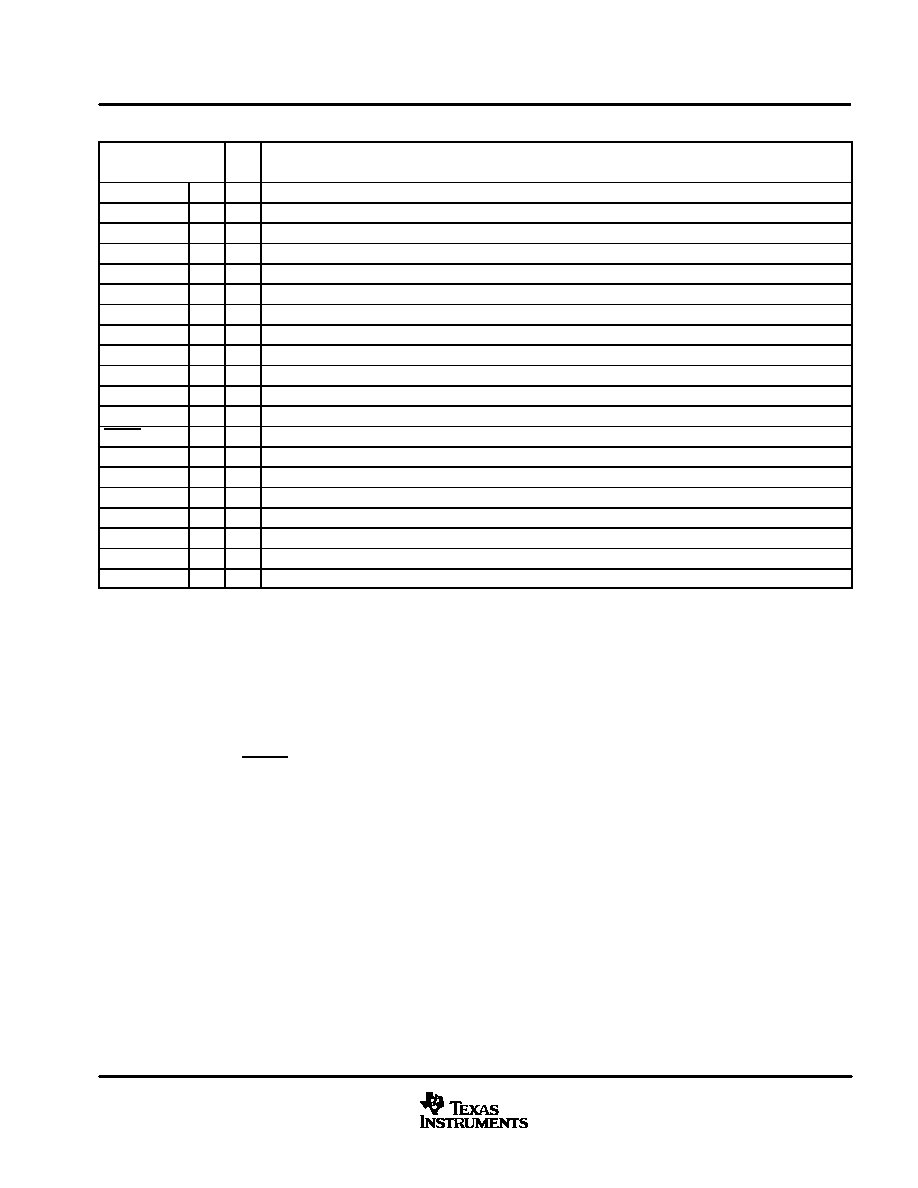
Terminal Functions
TERMINAL
I/O
DESCRIPTIONS
NAME
PIN
I/O
DESCRIPTIONS
AGND
6
Ł
Analog GND
BCK
11
I/O
Bit clock input/output
BYPAS
8
I
HPF bypass control. Low: normal mode (dc cut); High: bypass mode (through)
DGND
13
Ł
Digital GND
DOUT
12
O
Audio data output
FMT0
17
I
Audio data format select 0. See data format
FMT1
18
I
Audio data format select 1. See data format
FSYNC
9
I/O
Frame synchronous clock input/output
LRCK
10
I/O
Sampling clock input/output
MODE0
19
I
Mode select 0. See interface mode
MODE1
20
I
Mode select 1. See interface mode
OSR
16
I
Oversampling ratio select. Low:
ū
64 fS; High:
ū
128 fS
PDWN
7
I
Power-down control, active low
SCKI
15
I
System clock input; 256 fS, 384 fS, 512 fS or 768 fS¦
VCC
5
Ł
Analog power supply, 5 V
VDD
14
Ł
Digital power supply, 3.3 V
VINL
1
I
Analog input, L-channel
VINR
2
I
Analog input, R-channel
VREF1
3
Ł
Reference 1 decoupling capacitor
VREF2
4
Ł
Reference 2 voltage input, normally connected to VCC
Schmitt-trigger input with internal pulldown (50 k
typically), 5-V tolerant
Schmitt-trigger input
¦ Schmitt-trigger input, 5-V tolerant
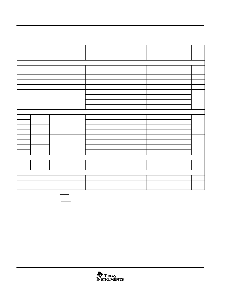
absolute maximum ratings over operating free-air temperature (unless otherwise noted)
Č
Supply voltage:
V
CC
6.5 V
. . . . . . . . . . . . . . . . . . . . . . . . . . . . . . . . . . . . . . . . . . . . . . . . . . . . . . . . . . . . . . . . . . . . . . . . .
V
DD
4.0 V
. . . . . . . . . . . . . . . . . . . . . . . . . . . . . . . . . . . . . . . . . . . . . . . . . . . . . . . . . . . . . . . . . . . . . . . . .
Ground voltage differences: AGND, DGND
▒
0.1 V
. . . . . . . . . . . . . . . . . . . . . . . . . . . . . . . . . . . . . . . . . . . . . . . . . . . . . . .
Digital input voltage: FSYNC, LRCK, BCK, DOUT
Ł0.3 V to (V
DD
+ 0.3 V)
. . . . . . . . . . . . . . . . . . . . . . . . . . . . . . . . . .
PDWN, BYPAS, SCKI, OSR, FMT0, FMT1, MODE0, MODE1
Ł0.3 V to 6.5 V
. . . . . . . . . . . .
Analog input voltage: V
IN
L, V
IN
R, V
REF
1, V
REF
2
Ł0.3 V to (V
CC
+ 0.3 V)
. . . . . . . . . . . . . . . . . . . . . . . . . . . . . . . . . .
Input current (any pins except supplies)
▒
10 mA
. . . . . . . . . . . . . . . . . . . . . . . . . . . . . . . . . . . . . . . . . . . . . . . . . . . . . . . . .
Ambient temperature under bias
Ł40
░
C to 125
░
C
. . . . . . . . . . . . . . . . . . . . . . . . . . . . . . . . . . . . . . . . . . . . . . . . . . . . . . .
Storage temperature
Ł55
░
C to 150
░
C
. . . . . . . . . . . . . . . . . . . . . . . . . . . . . . . . . . . . . . . . . . . . . . . . . . . . . . . . . . . . . . . . . .
Junction temperature
150
░
C
. . . . . . . . . . . . . . . . . . . . . . . . . . . . . . . . . . . . . . . . . . . . . . . . . . . . . . . . . . . . . . . . . . . . . . . . . .
Lead temperature (soldering)
260
░
C, 5 s
. . . . . . . . . . . . . . . . . . . . . . . . . . . . . . . . . . . . . . . . . . . . . . . . . . . . . . . . . . . . . . . .
Package temperature (IR reflow, peak)
260
░
C
. . . . . . . . . . . . . . . . . . . . . . . . . . . . . . . . . . . . . . . . . . . . . . . . . . . . . . . . . . .
Č Stresses beyond those listed under "absolute maximum ratings" may cause permanent damage to the device. These are stress ratings only, and
functional operation of the device at these or any other conditions beyond those indicated under "recommended operating conditions" is not
implied. Exposure to absolute-maximum-rated conditions for extended periods may affect device reliability.
PCM1802
SLES023B Ł DECEMBER 2001 Ł REVISED MARCH 2002
4
www.ti.com
electrical characteristics, all specifications at T
A
= 25
░
C, V
CC
= 5 V, V
DD
= 3.3 V, master mode,
f
S
= 44.1 kHz, system clock = 384 f
S
, over sampling ratio =
ū
128, 24-bit data (unless otherwise
noted)
TEST CONDITIONS
PCM1802DB
UNIT
TEST CONDITIONS
MIN
TYP
MAX
UNIT
Resolution
24
bits
DATA FORMAT
Audio data interface format
Left justified, I2S,
right justified
Audio data bit length
20, 24
bits
Audio data format
MSB first, 2s complement
fS
Sampling frequency
16
44.1
96
kHz
256 fS
4.096
11.2896
24.576
System clock frequency
384 fS
6.144
16.9344
36.864
MHz
System clock frequency
512 fS
8.192
22.5792
49.152
MHz
768 fS
12.288
33.8688
INPUT LOGIC
VIH
See Note 1
2
VDD
VIL
See Note 1
Input logic level
0
0.8
VDC
VIH
See Note 2
Input logic level
2
5.5
VDC
VIL
See Note 2
0
0.8
IIH
See Note 3
VIN = VDD
▒
10
IIL
See Note 3
Input logic current
VIN = 0 V
▒
10
A
IIH
See Note 4
Input logic current
VIN = VDD
65
100
Ą
A
IIL
See Note 4
VIN = 0 V
▒
10
OUTPUT LOGIC
VOH
See Note 5
Output logic level
IOUT = Ł1 mA
2.8
VDC
VOL
See Note 5
Output logic level
IOUT = 1 mA
0.5
VDC
DC ACCURACY
Gain mismatch channel-to-channel
▒
1
▒
4
%FSR
Gain error
▒
2
▒
6
%FSR
Bipolar zero error
LCF bypass (see Note 6)
▒
2
%FSR
NOTES:
1. Pins 9Ł11: FSYNC, LRCK, BCK (Schmitt-trigger input, in slave mode)
2. Pins 7Ł8, 15Ł20: PDWN, BYPAS, SCKI, OSR, FMT0, FMT1, MODE0, MODE1 (Schmitt-trigger input, 5-V tolerant).
3. Pins 9Ł11, 15: FSYNC, LRCK, BCK (Schmitt-trigger input in slave mode), SCKI (Schmitt-trigger input).
4. Pins 7Ł8, 16Ł20: PDWN, BYPAS, OSR, FMT0, FMT1, MODE0, MODE1 (Schmitt-trigger input, with 50-k
typical pulldown
resistor).
5. Pins 9Ł12: FSYNC, LRCK, BCK (in master mode), DOUT
6. Low cut filter
PCM1802
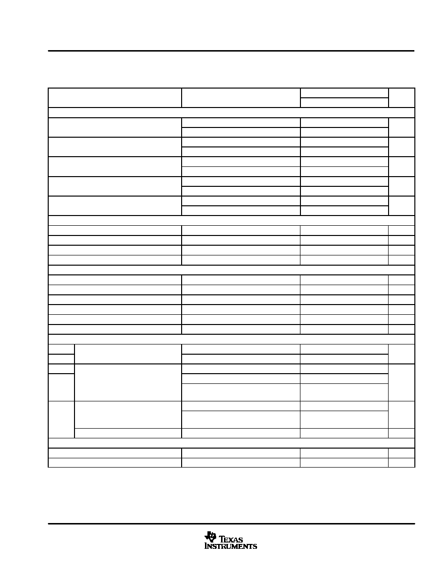
SLES023B Ł DECEMBER 2001 Ł REVISED MARCH 2002
5
www.ti.com
electrical characteristics, all specifications at T
A
= 25
░
C, V
CC
= 5 V, V
DD
= 3.3 V, master mode,
f
S
= 44.1 kHz, system clock = 384 f
S
, over sampling ratio =
ū
128, 24-bit data (unless otherwise
noted) (continued)
TEST CONDITIONS
PCM1802DB
UNIT
TEST CONDITIONS
MIN
TYP
MAX
UNIT
DYNAMIC PERFORMANCE (see Note 7)
THD+N (V
0 5 dB)
fS = 44.1 kHz
0.0015%
0.003%
THD+N (VIN = Ł0.5 dB)
fS = 96 kHz (see Note 8)
0.0025%
THD N (V
60 dB)
fS = 44.1 kHz
0.7%
THD+N (VIN = Ł60 dB)
fS = 96 kHz (see Note 8)
1.2%
Dynamic range
fS = 44.1 kHz, A-weighted
100
105
dB
Dynamic range
fS = 96 kHz, A-weighted (see Note 8)
103
dB
S/N ratio
fS = 44.1 kHz, A-weighted
100
105
dB
S/N ratio
fS = 96 kHz, A-weighted (see Note 8)
103
dB
Channel separation
fS = 44.1 kHz
96
103
dB
Channel separation
fS = 96 kHz (see Note 8)
98
dB
ANALOG INPUT
Input voltage
0.6 VCC
VpŁp
Center voltage (VREF1)
0.5 VCC
V
Input impedance
20
k
Antialiasing filter frequency response
Ł3 dB
300
kHz
DIGITAL FILTER PERFORMANCE
Passband
0.454 fS
Hz
Stopband
0.583 fS
Hz
Passband ripple
▒
0.05
dB
Stopband attenuation
Ł65
dB
Delay time
17.4/fS
s
HPF frequency response
Ł3 dB
0.019 fS
mHz
POWER SUPPLY REQUIREMENTS
VCC
Voltage range
4.5
5
5.5
VDC
VDD
Voltage range
2.7
3.3
3.6
VDC
ICC
VCC = 5 V, VDD = 3.3 V
24
30
Supply current (see Note 9)
fS = 44.1 kHz VCC = 5 V, VDD = 3.3 V
8.3
10
mA
IDD
Supply current (see Note 9)
fS = 96 kHz, VCC = 5 V, VDD = 3.3 V (see
Note 8)
17
mA
fS = 44.1 kHz, VCC = 5 V, VDD = 3.3 V
147
183
PD
Power dissipation; operation
fS = 96 kHz, VCC = 5 V, VDD = 3.3 V (see
Note 8)
176
mW
Power dissipation; power down
VCC = 5 V, VDD = 3.3 V
0.5
mW
TEMPERATURE RANGE
Operation temperature
Ł40
85
_
C
Thermal resistance (
JA)
20-pin SSOP
115
░
C/W
NOTES:
7. Analog performance specs are tested with System Two
audio measurement system by Audio Precision
, using 400-Hz HPF,
20-kHz LPF at 44.1-kHz operation, 40-kHz LPF at 96-kHz operation in RMS mode.
8. fS = 96 kHz, system clock = 256 fS, oversampling ratio =
ū
64.
9. Minimum load on DOUT (pin 12), BCK (pin 11), LRCK (pin 10), FSYNC (pin 9).

PCM1802
SLES023B Ł DECEMBER 2001 Ł REVISED MARCH 2002
6
www.ti.com
TYPICAL PERFORMANCE CURVES OF INTERNAL FILTER
digital filter--decimation filter frequency response
Figure 1. Overall Characteristics
Frequency [
ū
fS]
Ł200
Ł150
Ł100
Ł50
0
50
0
8
16
24
32
40
48
56
64
Oversampling Ratio = x128
Amplitude
Ł
dB
AMPLITUDE
vs
FREQUENCY
Figure 2. Overall Characteristics
Frequency [
ū
fS]
Ł200
Ł150
Ł100
Ł50
0
50
0
8
16
24
32
Amplitude
Ł
dB
AMPLITUDE
vs
FREQUENCY
Oversampling Ratio = x64
Figure 3. Stopband Attenuation Characteristics
Frequency [
ū
fS]
Ł100
Ł90
Ł80
Ł70
Ł60
Ł50
Ł40
Ł30
Ł20
Ł10
0
0.00
0.25
0.50
0.75
1.00
Amplitude
Ł
dB
AMPLITUDE
vs
FREQUENCY
Oversampling
Ratio = x128 and x64
Figure 4. Passband Ripple Characteristics
Frequency [
ū
fS]
Ł1.0
Ł0.8
Ł0.6
Ł0.4
Ł0.2
Ł0.0
0.2
0.0
0.1
0.2
0.3
0.4
0.5
0.6
Amplitude
Ł
dB
AMPLITUDE
vs
FREQUENCY
Oversampling
Ratio = x128 and x64
All specifications at TA = 25
░
C, VCC = 5 V, VDD = 3.3 V, master mode, fS = 44.1 kHz, system clock = 384 fS, oversampling ratio =
ū
128,
24-bit data, unless otherwise noted.

PCM1802
SLES023B Ł DECEMBER 2001 Ł REVISED MARCH 2002
7
www.ti.com
TYPICAL PERFORMANCE CURVES OF INTERNAL FILTER
HPF (low cut filter) frequency response
Figure 5. LCF Stopband Characteristics
Frequency [
ū
fS/1000]
Ł100
Ł90
Ł80
Ł70
Ł60
Ł50
Ł40
Ł30
Ł20
Ł10
0
0.0
0.1
0.2
0.3
0.4
Amplitude
Ł
dB
AMPLITUDE
vs
FREQUENCY
Figure 6. LCF Passband Characteristics
Frequency [
ū
fS/1000]
Ł1.0
Ł0.8
Ł0.6
Ł0.4
Ł0.2
Ł0.0
0.2
0
1
2
3
4
Amplitude
Ł
dB
AMPLITUDE
vs
FREQUENCY
analog filter--antialiasing filter frequence response
Figure 7. Antialias Filter Stopband Characteristics
Ł50
Ł45
Ł40
Ł35
Ł30
Ł25
Ł20
Ł15
Ł10
Ł5
0
f Ł Frequency Ł Hz
Amplitude
Ł
dB
AMPLITUDE
vs
FREQUENCY
100
1k
10k
10M
100k
1M
Figure 8. Antialias Filter Passband Characteristics
Ł1.0
Ł0.9
Ł0.8
Ł0.7
Ł0.6
Ł0.5
Ł0.4
Ł0.3
Ł0.2
Ł0.1
Ł0.0
f Ł Frequency Ł Hz
Amplitude
Ł
dB
AMPLITUDE
vs
FREQUENCY
1
10
100
100k
1k
10k
All specifications at TA = 25
░
C, VCC = 5 V, VDD = 3.3 V, master mode, fS = 44.1 kHz, system clock = 384 fS, oversampling ratio =
ū
128,
24-bit data, unless otherwise noted.
PCM1802
SLES023B Ł DECEMBER 2001 Ł REVISED MARCH 2002
8
www.ti.com
TYPICAL PERFORMANCE CURVES
Figure 9
0.01
0.02
0.03
0.04
Ł50
Ł25
0
25
50
75
100
TA Ł Free-Air Temperature Ł
░
C
THD+N
Ł
T
otal Harmonic Distortion + Noise
Ł
%
TOTAL HARMONIC DISTORTION + NOISE
vs
FREE-AIR TEMPERATURE
0.004
0.003
0.002
0.001
Figure 10
100
101
102
103
104
105
106
107
108
109
110
Ł50
Ł25
0
25
50
75
100
TA Ł Free-Air Temperature Ł
░
C
Dynamic Range and SNR
Ł
dB
DYNAMIC RANGE and SNR
vs
FREE-AIR TEMPERATURE
SNR
Dynamic Range
Figure 11
0.01
0.02
0.03
0.04
4.25
4.50
4.75
5.00
5.25
5.50
5.75
VCC Ł Supply Voltage Ł V
THD+N
Ł
T
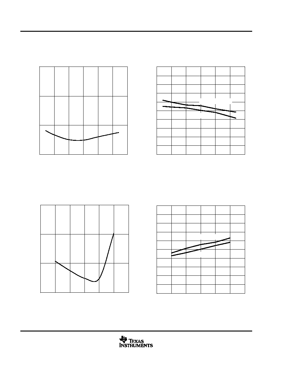
otal Harmonic Distortion + Noise
Ł
%
TOTAL HARMONIC DISTORTION + NOISE
vs
SUPPLY VOLTAGE
0.004
0.003
0.002
0.001
Figure 12
100
101
102
103
104
105
106
107
108
109
110
4.25
4.50
4.75
5.00
5.25
5.50
5.75
VCC Ł Supply Voltage Ł V
Dynamic Range and SNR
Ł
dB
DYNAMIC RANGE and SNR
vs
SUPPLY VOLTAGE
SNR
Dynamic Range
All specifications at TA = 25
░
C, VCC = 5.0 V, VDD = 3.3 V, master mode, fS = 44.1 kHz, system clock = 384 fS, oversampling ratio =
ū
128,
24-bit data, unless otherwise noted.

PCM1802
SLES023B Ł DECEMBER 2001 Ł REVISED MARCH 2002
9
www.ti.com
TYPICAL PERFORMANCE CURVES
Figure 13
0.01
0.02
0.03
0.04
0
10
20
30
40
fSAMPLE Condition Ł kHz
THD+N
Ł
T
otal Harmonic Distortion + Noise
Ł
%
TOTAL HARMONIC DISTORTION + NOISE
vs
f
SAMPLE
CONDITION
0.004
0.003
0.002
0.001
44.1
96
48
fS = 48 kHz, System Clock = 256 fS,
Oversampling Ratio =
ū
128.
fS = 96 kHz, System Clock = 256 fS,
Oversampling Ratio =
ū
64.
Figure 14
100
101
102
103
104
105
106
107
108
109
110
0
10
20
30
40
Dynamic Range and SNR
Ł
dB
DYNAMIC RANGE and SNR
vs
f
SAMPLE
CONDITION
44.1
96
48
SNR
Dynamic Range
fSAMPLE Condition Ł kHz
fS = 48 kHz, System Clock = 256 fS,
Oversampling Ratio =
ū
128.
fS = 96 kHz, System Clock = 256 fS,
Oversampling Ratio =
ū
64.
output spectrum
Figure 15
f Ł Frequency Ł kHz
Ł140
Ł120
Ł100
Ł80
Ł60
Ł40
Ł20
0
0
5
10
15
20
Input Level = Ł0.5 dB
Data Points = 8192
Amplitude
Ł
dB
AMPLITUDE
vs
FREQUENCY
Figure 16
f Ł Frequency Ł kHz
Ł140
Ł120
Ł100
Ł80
Ł60
Ł40
Ł20
0
0
5
10
15
20
Amplitude
Ł
dB
AMPLITUDE
vs
FREQUENCY
Input Level = Ł60 dB
Data Points = 8192
All specifications at TA = 25
░
C, VCC = 5 V, VDD = 3.3 V, master mode, fS = 44.1 kHz, system clock = 384 fS, oversampling ratio =
ū
128,
24-bit data, unless otherwise noted.
PCM1802
SLES023B Ł DECEMBER 2001 Ł REVISED MARCH 2002
10
www.ti.com
TYPICAL PERFORMANCE CURVES
Ł100 Ł90 Ł80 Ł70 Ł60 Ł50 Ł40 Ł30 Ł20 Ł10
0
Signal Level Ł dB
THD+N
Ł
T
otal Harmonic Distortion + Noise
Ł
%
TOTAL HARMONIC DISTORTION + NOISE
vs
SIGNAL LEVEL
100
1
0.1
0.01
0.001
10
Figure 17
supply current
0
5
10
15
20
25
30
0
10
20
30
40
I CC
and I
DD
Ł
Supply Current
Ł
mA
SUPPLY CURRENT
vs
f
SAMPLE
CONDITION
44.1
96
48
ICC
fSAMPLE Condition Ł kHz
IDD
fS = 48 kHz, System Clock = 256 fS,
Oversampling Ratio =
ū
128.
fS = 96 kHz, System Clock = 256 fS,
Oversampling Ratio =
ū
64.
Figure 18
All specifications at TA = +25
░
C, VCC = 5 V, VDD = 3.3 V, Master Mode, fS = 44.1 kHz, system clock = 384fS, oversampling ratio =
ū
128,
24-bit data, unless otherwise noted.
PCM1802
SLES023B Ł DECEMBER 2001 Ł REVISED MARCH 2002
11
www.ti.com
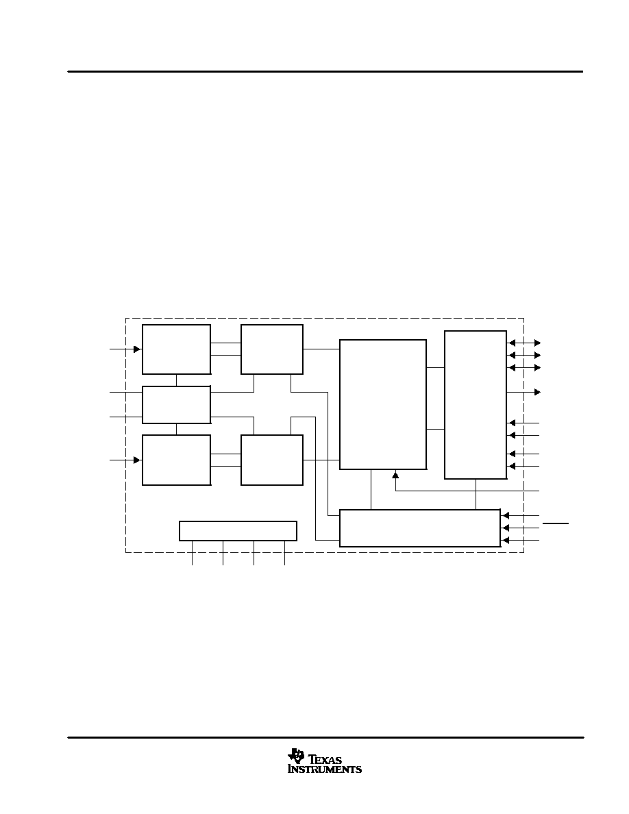
PRINCIPLES OF OPERATION
PCM1802 consists of a reference circuit, two channels of single-ended-to-differential converter, fifth-order
delta-sigma modulator with full differential architecture, decimation filter with low cut filter, and a serial interface
circuit. Figure 19 illustrates the total architecture of PCM1802, Figure 20 illustrates the architecture of
single-ended-to-differential converter and antialiasing filter, and Figure 21 illustrates the block diagram of
fifth-order delta-sigma modulator and transfer function. An on-chip high-precision reference with one external
capacitor provides all reference voltages that are needed in the PCM1802, and defines the full scale voltage
range for both channels. On-chip single-ended-to-differential signal converters save the design, space, and
extra parts cost for external signal converters. Full differential architecture provides a wide dynamic range and
excellent power supply rejection performance. The input signal is sampled at a
ū
64 or
ū
128 oversampling rate,
thus eliminating an external sample-hold amplifier. A fifth-order delta-sigma noise shaper, which consists of five
integrators using the switched capacitor technique and a comparator, shapes the quantization noise generated
by the comparator and 1-bit DAC outside of the audio signal band. The high-order delta-sigma modulation
randomizes the modulator outputs and reduces the idle tone level. The 64-f
S
or 128-f
S
, 1-bit stream from the
delta-sigma modulator is converted to a 1-f
S
, 24-bit or 20-bit digital signal by removing high-frequency noise
components with a decimation filter. The dc component of the signal is removed by the LCF, and the LCF output
is converted to a time-multiplexed serial signal through the serial interface, which provides flexible serial
formats.
Single-End
/Differential
Converter
BCK
VINL
Reference
Single-End
/Differential
Converter
VREF1
VREF2
VINR
5th Order
Delta-Sigma
Modulator
5th Order
Delta-Sigma
Modulator
ū
1/64 (
ū
1/128)
Decimation
Filter with
DC Cut Filter
Power Supply
AGND
VCC
VDD
DGND
Clock and Timing Control
Serial
Interface
Mode/
Format
Control
LRCK
FSYNC
DOUT
FMT0
FMT1
MODE0
MODE1
BYPAS
OSR
PDWN
SCKI
Figure 19. Block Diagram

PCM1802
SLES023B Ł DECEMBER 2001 Ł REVISED MARCH 2002
12
www.ti.com
PRINCIPLES OF OPERATION
VINL
1
3
4
VREF1
VREF2
0.1
Ą
F
+
1
Ą
F
20 k
+
Ł
+
Ł
Delta-Sigma
Modulator
(+)
(Ł)
Reference
5
VCC
+
10
Ą
F
Figure 20. Analog Front End (Left Channel)
1st
SW-CAP
Integrator
Analog
In
X(z)
+
Ł
+
Ł
2nd
SW-CAP
Integrator
3rd
SW-CAP
Integrator
+
Ł
4th
SW-CAP
Integrator
+
+
+
+
+
+
+
+
5th
SW-CAP
Integrator
Digital
Out
Y(z)
Comparator
Qn(z)
H(z)
1-Bit
DAC
STF(z) = H(z) / [1 + H(z)]
NTF(z) = 1 / [1 + H(z)]
Y(z) = STF(z) * X(z) + NTF(z) * Qn(z)
Signal Transfer Function
Noise Transfer Function
Figure 21. Block Diagram of Fifth-Order Delta-Sigma Modulator

PCM1802
SLES023B Ł DECEMBER 2001 Ł REVISED MARCH 2002
13
www.ti.com
PRINCIPLES OF OPERATION
system clock
The PCM1802 supports 256 f
S
, 384 f
S
, 512 f
S
, and 768 f
S
as the system clock, where f
S
is the audio sampling
frequency. The system clock must be supplied on SCKI (pin 15).
The PCM1802 has a system clock detection circuit which automatically senses if the system clock is operating
at 256 f
S
, 384 f
S
, 512 f
S
, or 768 f
S
in slave mode. In master mode, the system clock frequency must be selected
by MODE0 (pin 19) and MODE1 (pin 20), and 768 f
S
is not available. For system clock inputs of 384 f
S
, 512 f
S
,
and 768 f
S
, the system clock is divided to 256 f
S
automatically, and the 256 f
S
clock is used to operate the
delta-sigma modulator and the digital filter.
Table 1 shows the relationship of typical sampling frequencies and system clock frequencies, and Figure 22
shows system clock timing.
Table 1. Sampling Frequency and System Clock Frequency
SAMPLING RATE
FREQUENCY
SYSTEM CLOCK FREQUENCY (MHz)
FREQUENCY
(kHz)
256 fS
384 fS
512 fS
768 fS
32
8.192
12.288
16.384
24.576
44.1
11.2896
16.9344
22.5792
33.8688
48
12.288
18.432
24.576
36.864
64
16.384
24.576
32.768
49.152
88.2
22.5792
33.8688
45.1584
--
96
24.576
36.864
49.152
--
SCKI
0.8 V
SCKI
2.0 V
tSCKL
tSCKH
PARAMETER
MIN
MAX
UNIT
tSCKH
System clock pulse width, high
7
ns
tSCKL
System clock pulse width, low
7
ns
Figure 22. System Clock Timing

PCM1802
SLES023B Ł DECEMBER 2001 Ł REVISED MARCH 2002
14
www.ti.com
PRINCIPLES OF OPERATION
power-on reset sequence
The PCM1802 has an internal power-on reset circuit and initialization (reset) is performed automatically when
the power supply (V
DD
) exceeds 2.2 V (typ). While V
DD
< 2.2 V (typ), and for 1024 system-clock counts after
V
DD
> 2.2 V (typ), the PCM1802 stays in the reset state and the digital output is forced to zero. The digital output
is valid after the reset state is released and the time of 4480/f
S
has passed. Figure 23 illustrates the internal
power-on reset timing and the digital output for power-on reset.
System Clock
2.6 V
2.2 V
1.8 V
Internal Reset
DOUT
Zero Data
Normal Data
Reset
VDD
Reset Removal
1024 System Clocks
4480 / fS
Figure 23. Internal Power-On Reset Timing
serial audio data interface
The PCM1802 interfaces with the audio system through BCK (pin 11), LRCK (pin 10), FSYNC (pin 9), and DOUT
(pin 12).
PCM1802
SLES023B Ł DECEMBER 2001 Ł REVISED MARCH 2002
15
www.ti.com
PRINCIPLES OF OPERATION
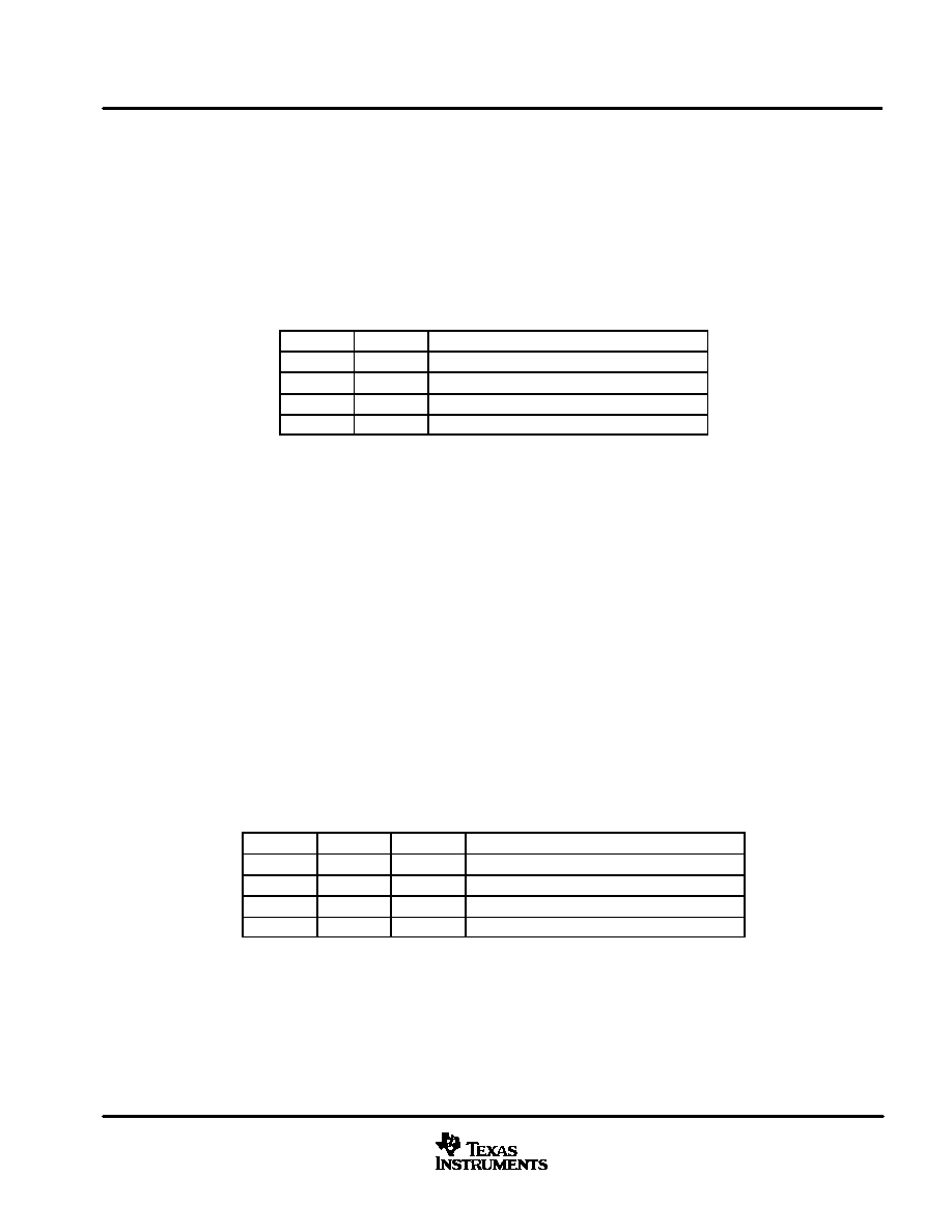
interface mode
The PCM1802 supports master mode and slave mode as interface modes, and they are selected by MODE1
(pin 20) and MODE0 (pin 19) as shown in Table 2.
In master mode, the PCM1802 provides the timing for serial audio data communications between the PCM1802
and the digital audio processor or external circuit. In slave mode, the PCM1802 receives the timing for data
transfer from an external controller.
Table 2. Interface Mode
MODE1
MODE0
INTERFACE MODE
0
0
Slave mode (256 fS, 384 fS, 512 fS, 768 fS)
0
1
Master mode (512 fS)
1
0
Master mode (384 fS)
1
1
Master mode (256 fS)
(1) Master mode
In master mode, BCK, LRCK and FSYNC work as output pins, and these pins are controlled by timing which
is generated in the clock circuit of the PCM1802. FSYNC is used to designate the valid data from the
PCM1802. The rising edge of FSYNC indicates the starting point of the converted audio data and the falling
edge of this signal indicates the ending point of the data. The frequency of this signal is fixed at 2
ū
LRCK.
The duty cycle ratio depends on data bit length. The frequency of BCK is fixed at 64
ū
LRCK. The 768 f
S
system clock is not available in master mode.
(2) Slave mode
In slave mode, BCK, LRCK and FSYNC work as input pins. FSYNC is used to enable the BCK signal, and
the PCM1802 can shift out the converted data while FSYNC is HIGH. The PCM1802 accepts either the
64 BCK/LRCK or the 48 BCK/LRCK format. The delay of FSYNC from the LRCK transition must be within
16 BCKs for the 64 BCK/LRCK format and within 12 BCKs for the 48 BCK/LRCK format.
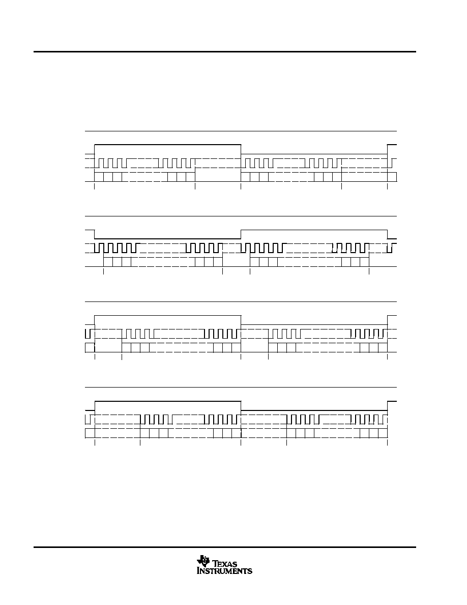
data format
The PCM1802 supports four audio data formats in both master and slave modes, and they are selected by FMT1
(pin 18) and FMT0 (pin 17) as shown in Table 3. Figure 24 and Figure 26 illustrate the data formats in slave
mode and master mode, respectively.
Table 3. Data Format
FORMAT#
FMT1
FMT0
FORMAT
0
0
0
Left justified, 24 bit
1
0
1
I2S, 24 bit
2
1
0
Right justified, 24 bit
3
1
1
Right justified, 20 bit
PCM1802
SLES023B Ł DECEMBER 2001 Ł REVISED MARCH 2002
16
www.ti.com
PRINCIPLES OF OPERATION
interface timing
Figure 25 and Figure 27 illustrate the interface timing in slave mode and master mode, respectively.
FORMAT 0: FMT[1:0] = 00
24-Bit, MSB-First, Left-Justified
BCK
LRCK
Right-Channel
Left-Channel
DOUT
1
22 23 24
3
2
1
MSB
LSB
22 23 24
3
2
1
MSB
LSB
FSYNC
FORMAT 1: FMT[1:0] = 01
24-Bit, MSB-First, IIS
LRCK
Right-Channel
Left-Channel
BCK
DOUT
22 23 24
3
2
1
MSB
LSB
22 23 24
3
2
1
MSB
LSB
FSYNC
FORMAT 2: FMT[1:0] = 10
24-Bit, MSB-First, Right-Justified
LRCK
Right-Channel
Left-Channel
BCK
DOUT
24
22 23 24
3
2
1
MSB
LSB
22 23 24
3
2
1
MSB
LSB
FSYNC
FORMAT 3: FMT[1:0] = 11
20-Bit, MSB-First, Right-Justified
LRCK
Right-Channel
Left-Channel
BCK
DOUT
20
18 19 20
3
2
1
MSB
LSB
18 19 20
3
2
1
MSB
LSB
FSYNC
Figure 24. Audio Data Format (Slave Mode: FSYNC, LRCK, BCK Work as Inputs)

PCM1802
SLES023B Ł DECEMBER 2001 Ł REVISED MARCH 2002
17
www.ti.com
PRINCIPLES OF OPERATION
interface timing (continued)
BCK
FSYNC
LRCK
DOUT
t(FSSU)
t(BCKH)
t(BCKL)
t(LRHD)
t(FSHD)
t(LRCP)
t(LRSU)
t(BCKP)
t(CKDO)
t(LRDO)
1.4 V
1.4 V
1.4 V
0.5 VDD
PARAMETER
MIN
TYP
MAX
UNIT
t(BCKP)
BCK period
150
ns
t(BCKH)
BCK pulse duration high
60
ns
t(BCKL)
BCK pulse duration low
60
ns
t(LRSU)
LRCK setup time to BCK rising edge
40
ns
t(LRHD)
LRCK hold time to BCK rising edge
20
ns
t(LRCP)
LRCK period
10
Ą
s
t(FSSU)
FSYNC setup time to BCK rising edge
20
ns
t(FSHD)
FSYNC hold time to BCK rising edge
20
ns
t(CKDO)
Delay time, BCK falling edge to DOUT valid
Ł10
20
ns
t(LRDO)
Delay time, LRCK edge to DOUT valid
Ł10
20
ns
tr
Rise time of all signals
10
ns
tf
Fall time of all signals
10
ns
NOTE: Timing measurement reference level is (VIH/VIL)/2. Rise and fall times are measured from 10% to 90% of IN/OUT signal swing. Load
capacitance of DOUT is 20 pF.
Figure 25. Audio Data Interface Timing (Slave Mode: FSYNC, LRCK, BCK Work as Inputs)

PCM1802
SLES023B Ł DECEMBER 2001 Ł REVISED MARCH 2002
18
www.ti.com
PRINCIPLES OF OPERATION
interface timing (continued)
FORMAT 0: FMT[1:0] = 00
24-Bit, MSB-First, Left-Justified
BCK
LRCK
Right-Channel
Left-Channel
DOUT
1
22 23 24
3
2
1
MSB
LSB
22 23 24
3
2
1
MSB
LSB
FSYNC
FORMAT 1: FMT[1:0] = 01
24-Bit, MSB-First, IIS
LRCK
Right-Channel
Left-Channel
BCK
DOUT
22 23 24
3
2
1
MSB
LSB
22 23 24
3
2
1
MSB
LSB
FSYNC
FORMAT 2: FMT[1:0] = 10
24-Bit, MSB-First, Right-Justified
LRCK
Right-Channel
Left-Channel
BCK
DOUT
24
22 23 24
3
2
1
MSB
LSB
22 23 24
3
2
1
MSB
LSB
FSYNC
FORMAT 3: FMT[1:0] = 11
20-Bit, MSB-First, Right-Justified
LRCK
Right-Channel
Left-Channel
BCK
DOUT
20
18 19 20
3
2
1
MSB
LSB
18 19 20
3
2
1
MSB
LSB
FSYNC
Figure 26. Audio Data Format (Master Mode: FSYNC, LRCK, BCK Work as Outputs)

PCM1802
SLES023B Ł DECEMBER 2001 Ł REVISED MARCH 2002
19
www.ti.com
PRINCIPLES OF OPERATION
interface timing (continued)
BCK
FSYNC
LRCK
DOUT
t(CKFS)
t(BCKH)
t(BCKL)
t(CKLR)
t(LRCP)
t(BCKP)
t(CKDO)
t(LRDO)
0.5 VDD
0.5 VDD
0.5 VDD
0.5 VDD
t(FSYP)
PARAMETER
MIN
TYP
MAX
UNIT
t(BCKP)
BCK period
150
1/(64 fS)
1200
ns
t(BCKH)
BCK pulse width high
75
600
ns
t(BCKL)
BCK pulse width low
75
600
ns
t(CKLR)
Delay time BCK falling edge to LRCK valid
Ł10
20
ns
t(LRCP)
LRCK period
10
1/ fS
80
Ą
s
t(CKFS)
Delay time BCK falling edge to FSYNC valid
Ł10
20
ns
t(FSYP)
FSYNC period
5
1/(2 fS)
40
Ą
s
t(CKDO)
Delay time, BCK falling edge to DOUT valid
Ł10
20
ns
t(LRDO)
Delay time, LRCK edge to DOUT valid
Ł10
20
ns
tr
Rise time of all signals
10
ns
tf
Fall time of all signals
10
ns
NOTE: Timing measurement reference level is (VIH/VIL) / 2. Rise and fall times are measured from 10% to 90% of IN/OUT signal swing. Load
capacitance of all signals is 20 pF.
Figure 27. Audio Data Interface Timing (Master Mode: FSYNC, LRCK, BCK Work as Outputs)

PCM1802
SLES023B Ł DECEMBER 2001 Ł REVISED MARCH 2002
20
www.ti.com
PRINCIPLES OF OPERATION
synchronization with digital audio system
In slave mode, the PCM1802 operates under LRCK, synchronized with system clock SCKI. The PCM1802 does
not need a specific phase relationship between LRCK and SCKI, but does require the synchronization of LRCK
and SCKI.
If the relationship between LRCK and SCKI changes more than
▒
6 BCKs for 64 BCK/frame (
▒
5 BCKs for
48 BCK/frame) during one sample period due to LRCK or SCKI jitter, internal operation of the ADC halts within
1/f
S
and digital output is forced into BPZ code until re-synchronization between LRCK and SCKI is completed.
In the case of changes less than
▒
5 BCKs for 64 BCK/frame (
▒
4 BCKs for 48 BCK/frame), resynchronization
does not occur.
Figure 28 illustrates digital output response for loss of synchronization and resynchronization. During undefined
data, some noise might be generated in the audio signal. Also, the transition of normal to undefined data and
undefined or zero data to normal creates a data discontinuity in the digital output, which can generate some
noise in the audio signal.
It is recommended to set PDWN low to get stable analog performance when the sampling rate, interface mode,
data format, or oversampling control is changed.
1/fS
32/fS
NORMAL DATA
ZERO DATA
UNDEFINED
DATA
NORMAL DATA
SYNCHRONOUS
ASYNCHRONOUS
SYNCHRONOUS
Resynchronization
Synchronization Lost
DOUT
State of Synchronization
Figure 28. ADC Digital Output for Loss of Synchronization and Resynchronization
power down, LCF bypass, oversampling control
PDWN (pin 7) controls the entire ADC operation. During power-down mode, both the supply current for the
analog portion and the clock signal for the digital portion are shut down, and power dissipation is minimized.
Also, DOUT (pin 12) is disabled and no system clock is accepted during power-down mode.
Table 4. Power-Down Control
PDWN
Power-down mode
LOW
Power-down mode
HIGH
Normal operation mode
The built-in function for dc component rejection can be bypassed using the BYPAS (pin 8) control. In bypass
mode, the dc components of the analog input signal, internal dc offset, etc., are also converted and included
in the digital output data.
Table 5. LCF Bypass Control
BYPAS
LCF (low-cut filter) mode
LOW
Normal (no dc component on DOUT) mode
HIGH
Bypass (dc component on DOUT) mode

PCM1802
SLES023B Ł DECEMBER 2001 Ł REVISED MARCH 2002
21
www.ti.com
PRINCIPLES OF OPERATION
power down, LCF bypass, oversampling control (continued)
OSR (pin 16) controls the oversampling ratio of the delta-sigma modulator,
ū
64 or
ū
128. The
ū
128 mode is
available for f
S
< 50 kHz, and must be used carefully as performance is affected by the duty cycle of the 384 f
S
system clock.
Table 6. Oversampling Control
OSR
Oversampling ratio
LOW
ū
64
HIGH
ū
128 (fS < 50 kHz)
APPLICATION INFORMATION
typical circuit connection diagram
Figure 29 illustrates a typical circuit connection diagram in which the cutoff frequency of the input HPF is about
8 Hz.
VINL
20
19
18
17
16
15
14
13
12
11
1
2
3
4
5
6
7
8
9
10
PCM1802
VINR
VREF1
VREF2
VCC
AGND
PDWN
BYPAS
FSYNC
LRCK
MODE1
DGND
MODE0
FMT1
FMT0
OSR
DOUT
BCK
VDD
SCKI
+
Oversampling
System Clock
L-Ch IN
R-Ch IN
0 V
5 V
C4
+
C5¦
Power Down
LCF Bypass
Control
+
C3
L/R Clock
Frame Sync.
Audio Data
Processor
Mode [1:0]
Format [1:0]
3.3 V
0 V
Data Clock
Data Out
+
C1
+
C2
Control
+
C6
W
R1#
C1, C2: A 1-
Ą
F capacitor gives 8-Hz (
= 1
Ą
F
ū
20 k
) cutoff frequency for input HPF in normal operation, and requires a power-on settling
time with 20-ms time constant in the power-on initialization period.
C3, C4: Bypass capacitors, 0.1-
Ą
F ceramic and 10-
Ą
F tantalum, depending on layout and power supply.
¦ C5: 0.1-
Ą
F ceramic and 4.7-
Ą
F tantalum capacitors are recommended.
Č C6: 0.1-
Ą
F ceramic and 4.7-
Ą
F tantalum capacitors are recommended for using a noise analog power supply. These capacitor are not required
for clean analog supply.
# R1: 1-k
resistor is recommended for using a noisy analog power supply. This resistor is shorted for a clean analog supply.
Figure 29. Typical Circuit Connection

PCM1802
SLES023B Ł DECEMBER 2001 Ł REVISED MARCH 2002
22
www.ti.com
APPLICATION INFORMATION
board design and layout considerations
V
CC
, V
DD
pins
The digital and analog power supply lines to the PCM1802 should be bypassed to the corresponding ground
pins with 0.1-
Ą
F ceramic and 10-
Ą
F tantalum capacitors as close to the pins as possible to maximize the
dynamic performance of the ADC.
AGND, DGND pins
To maximize the dynamic performance of the PCM1802, the analog and digital grounds are not connected
internally. These grounds should have very low impedance to avoid digital noise feeding back into the analog
ground. They should be connected directly to each other under the parts to reduce the potential noise problem.
V
IN
pins
A 1-
Ą
F capacitor is recommended as an ac-coupling capacitor which gives 8-Hz cutoff frequency. If a higher
full-scale input voltage is required, it can be accommodated by adding only one series resistor to each V
IN
pin.
V
REF
1 pin
A 0.1-
Ą
F ceramic and 10-
Ą
F chemical capacitors are recommended between V
REF
1 and AGND to insure low
source impedance of ADC references. These capacitors should be located as close as possible to the V
REF
1
pin to reduce the dynamic errors on ADC references.
V
REF
2 pin
The differential voltage between V
REF
2 and AGND sets the analog input full-scale range. A 0.1-
Ą
F ceramic and
10-
Ą
F chemical capacitors are recommended between V
REF
2 and AGND with insertion of a 1-k
resistor
between VCC and VREF2 for using a noisy analog power supply. These capacitors and resistor are not required
for clean analog supply. These capacitors should be located as close as possible to the V
REF
2 pin to reduce
the dynamic errors on ADC references. Full-scale input level is affected by this 1-k
resistor and decreases
by 3%.
DOUT pin
The DOUT pin has enough load drive capability, but locating a buffer near the PCM1802 and minimizing load
capacitance is recommended if the DOUT line is long, in order to minimize the digital-analog crosstalk and
maximize the dynamic performance of the ADC.
system clock
The quality of the system clock can influence dynamic performance, as the PCM1802 operates based on the
system clock. In slave mode, it may be necessary to consider the system-clock duty cycle, jitter, and the time
difference between the system clock transition and the BCK or LRCK transition.
PCM1802
SLES023B Ł DECEMBER 2001 Ł REVISED MARCH 2002
23
www.ti.com
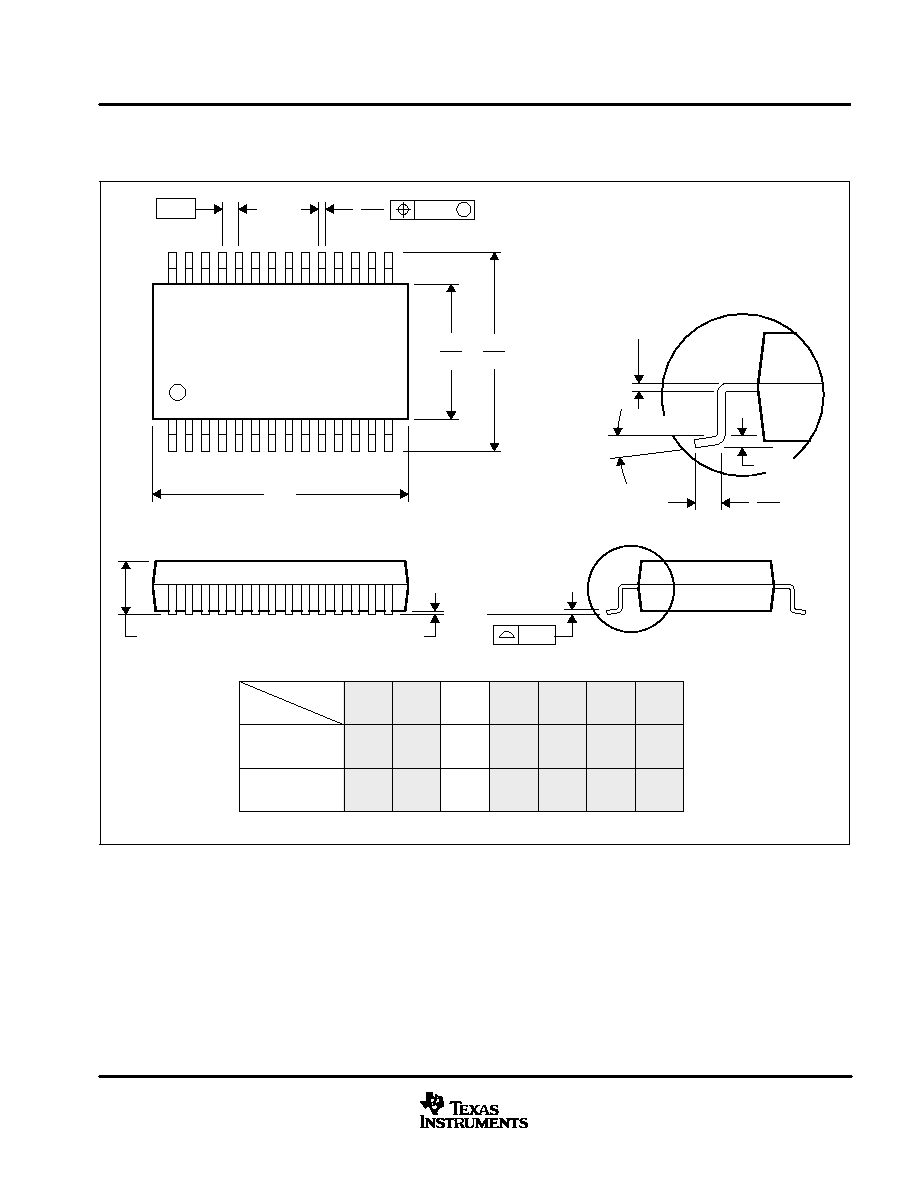
MECHANICAL DATA
DB (R-PDSO-G**)
PLASTIC SMALL-OUTLINE
4040065 /D 09/00
28 PINS SHOWN
Gage Plane
8,20
7,40
0,15 NOM
0,55
0,95
0,25
38
12,90
12,30
28
10,50
24
8,50
Seating Plane
9,90
7,90
30
10,50
9,90
0,38
5,60
5,00
15
0,22
14
A
28
1
20
16
6,50
6,50
14
0,05 MIN
5,90
5,90
DIM
A MAX
A MIN
PINS **
2,00 MAX
6,90
7,50
0,65
M
0,15
0
░
Ł 8
░
0,10
NOTES: A. All linear dimensions are in millimeters.
B. This drawing is subject to change without notice.
C. Body dimensions do not include mold flash or protrusion not to exceed 0,15.
D. Falls within JEDEC MO-150

IMPORTANT NOTICE
Texas Instruments Incorporated and its subsidiaries (TI) reserve the right to make corrections, modifications,
enhancements, improvements, and other changes to its products and services at any time and to discontinue
any product or service without notice. Customers should obtain the latest relevant information before placing
orders and should verify that such information is current and complete. All products are sold subject to TI's terms
and conditions of sale supplied at the time of order acknowledgment.
TI warrants performance of its hardware products to the specifications applicable at the time of sale in
accordance with TI's standard warranty. Testing and other quality control techniques are used to the extent TI
deems necessary to support this warranty. Except where mandated by government requirements, testing of all
parameters of each product is not necessarily performed.
TI assumes no liability for applications assistance or customer product design. Customers are responsible for
their products and applications using TI components. To minimize the risks associated with customer products
and applications, customers should provide adequate design and operating safeguards.
TI does not warrant or represent that any license, either express or implied, is granted under any TI patent right,
copyright, mask work right, or other TI intellectual property right relating to any combination, machine, or process
in which TI products or services are used. Information published by TI regarding thirdŁparty products or services
does not constitute a license from TI to use such products or services or a warranty or endorsement thereof.
Use of such information may require a license from a third party under the patents or other intellectual property
of the third party, or a license from TI under the patents or other intellectual property of TI.
Reproduction of information in TI data books or data sheets is permissible only if reproduction is without
alteration and is accompanied by all associated warranties, conditions, limitations, and notices. Reproduction
of this information with alteration is an unfair and deceptive business practice. TI is not responsible or liable for
such altered documentation.
Resale of TI products or services with statements different from or beyond the parameters stated by TI for that
product or service voids all express and any implied warranties for the associated TI product or service and
is an unfair and deceptive business practice. TI is not responsible or liable for any such statements.
Mailing Address:
Texas Instruments
Post Office Box 655303
Dallas, Texas 75265
Copyright
2002, Texas Instruments Incorporated