www.ti.com
FEATURES
APPLICATIONS
DESCRIPTION
PCM1680
SLES133 ş MARCH 2005
24-Bit, 192-kHz Sampling, Enhanced Multilevel, Delta-Sigma, Audio Digital-to-Analog
Converter
Ě
Single Power-Supply Operation: 5-V Analog,
5-V Digital
Ě
24-Bit Resolution
Ě
Package: 28-Lead SSOP (150 mil)
Ě
Analog Performance:
Ě
Pin-Compatible With PCM1780
ş Dynamic Range: 105 dB Typical
ş SNR: 105 dB Typical
ş THD+N: 0.002% Typical
Ě
Integrated A/V Receivers
ş Full-Scale Output: 3.9 Vp-p Typical
Ě
DVD Movie and Audio Players
Ě
4
Î
/8
Î
Oversampling Interpolation Filter:
Ě
HDTV Receivers
ş Stop-Band Attenuation: ş50 dB
Ě
Car Audio Systems
ş Pass-Band Ripple:
▒
0.04 dB
Ě
DVD Add-On Cards for High-End PCs
Ě
Sampling Frequency: 5 kHz to 200 kHz
Ě
Digital Audio Workstations
Ě
System Clock: 128 f
S
, 192 f
S
, 256 f
S
, 384 f
S
,
Ě
Other Multichannel Audio Systems
512 f
S
, 768 f
S
, or 1152 f
S
With Autodetect
Ě
Zero Flags for Selectable Channel
Combinations
The PCM1680 is a CMOS monolithic integrated
circuit
which
features
eight
24-bit
audio
digi-
Ě
Serial Port (SPI/I
2
C) for Mode Control
tal-to-analog converters and support circuitry in a
Ě
User-Programmable Functions:
small 28-lead SSOP. The digital-to-analog converters
ş Flexible Audio Data Formats
use TI's enhanced multilevel delta-sigma architecture
Ě
Right-Justified, I
2
S, and Left-Justified
to achieve excellent signal-to-noise performance and
a high tolerance to clock jitter.
Ě
16-, 18-, 20-, and 24-Bit Audio Data
The PCM1680 accepts industry-standard audio data
ş Digital Attenuation: Mode Selectable
formats with 16- to 24-bit audio data. Sampling rates
Ě
0 dB to ş63 dB, 0.5 dB/step
up to 200 kHz are supported. The PCM1680 provides
Ě
0 dB to ş100 dB, 1 dB/step
a full set of user-programmable functions through a
ş Soft Mute
serial control port, SPI or I
2
C.
ş Digital De-Emphasis
ş Digital Filter Rolloff: Sharp or Slow
Please be aware that an important notice concerning availability, standard warranty, and use in critical applications of Texas
Instruments semiconductor products and disclaimers thereto appears at the end of this data sheet.
System Two, Audio Precision are trademarks of Audio Precision, Inc.
All trademarks are the property of their respective owners.
PRODUCTION DATA information is current as of publication date.
Copyright ę 2005, Texas Instruments Incorporated
Products conform to specifications per the terms of the Texas
Instruments standard warranty. Production processing does not
necessarily include testing of all parameters.
www.ti.com
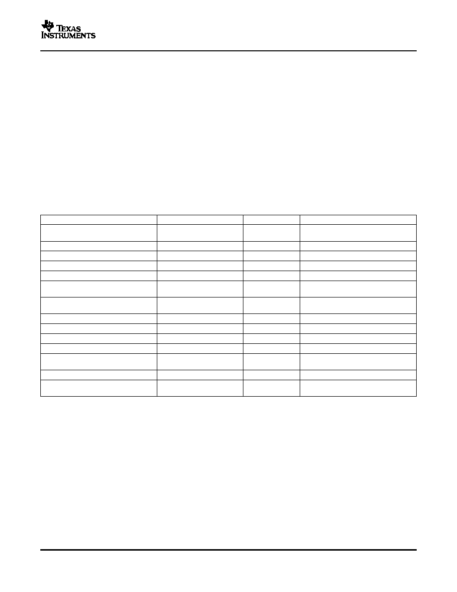
ABSOLUTE MAXIMUM RATINGS
RECOMMENDED OPERATING CONDITIONS
ELECTRICAL CHARACTERISTICS
PCM1680
SLES133 ş MARCH 2005
This integrated circuit can be damaged by ESD. Texas Instruments recommends that all integrated circuits be handled with
appropriate precautions. Failure to observe proper handling and installation procedures can cause damage. ESD damage can
range from subtle performance degradation to complete device failure. Precision integrated circuits may be more susceptible to
damage because very small parametric changes could cause the device not to meet its published specifications.
over operating free-air temperature range (unless otherwise noted)
(1)
PCM1680
Supply voltage: V
CC
1, V
CC
2, V
DD
ş0.3 V to 6.5 V
Supply voltage differences: V
CC
1, V
CC
2, V
DD
▒
0.1 V
Ground voltage differences: AGND1, AGND2, DGND
▒
0.1 V
Input voltage to digital pins
ş0.3 V to V
DD
+ 0.3 V, < 6.5 V
Input voltage to analog pins
ş0.3 V to V
CC
+ 0.3 V, < 6.5 V
Input current (any pins except supplies)
▒
10 mA
Operating temperature
ş40
░
C to 110
░
C
Storage temperature
ş55
░
C to 150
░
C
Junction temperature
150
░
C
Lead temperature (soldering)
260
░
C, 5 s
Package temperature (IR reflow, peak)
260
░
C
(1)
Stresses beyond those listed under "absolute maximum ratings" may cause permanent damage to the device. These are stress ratings
only, and functional operation of the device at these or any other conditions beyond those indicated under "recommended operating
conditions" is not implied. Exposure to absolute-maximum-rated conditions for extended periods may affect device reliability.
over operating free-air temperature range
MIN
NOM
MAX
UNIT
Analog supply voltage, V
CC
1, V
CC
2
4.75
5
5.25
V
Digital supply voltage, V
DD
4.75
5
5.25
V
Digital input logic family
TTL
System clock
8.192
36.864
MHz
Digital input clock frequency
Sampling clock
32
192
kHz
Analog output load resistance
5
k
Analog output load capacitance
50
pF
Digital output load capacitance
20
pF
Operating free-air temperature, T
A
ş25
70
░
C
all specifications at T
A
= 25
░
C, V
CC
= V
DD
= 5 V, f
S
= 48 kHz, system clock = 512 f
S
, and 24-bit data, unless otherwise noted
PARAMETER
TEST CONDITIONS
MIN
TYP
MAX
UNIT
RESOLUTION
24
Bits
DATA FORMAT
Audio data interface format
Right-justified, I
2
S, left-justified
Audio data bit length
16, 18, 20, or 24 bits, selectable
Audio data format
MSB-first, 2s complement
f
S
Sampling frequency
5
200
kHz
System clock frequency
128, 192, 256, 384,
512, 768, 1152 f
S
2
www.ti.com
PCM1680
SLES133 ş MARCH 2005
ELECTRICAL CHARACTERISTICS (continued)
all specifications at T
A
= 25
░
C, V
CC
= V
DD
= 5 V, f
S
= 48 kHz, system clock = 512 f
S
, and 24-bit data, unless otherwise noted
PARAMETER
TEST CONDITIONS
MIN
TYP
MAX
UNIT
DIGITAL INPUT/OUTPUT
Logic family
TTL compatible
V
IH
2
Input logic level
Vdc
V
IL
0.8
I
IH
(1)
V
IN
= V
CC
10
I
IL
(1)
V
IN
= 0 V
ş10
Input logic current
Á
A
I
IH
(2)
V
IN
= V
CC
65
100
I
IL
(2)
V
IN
= 0 V
ş10
V
OH
(3)
I
OH
= ş1 mA
2.4
Output logic level
Vdc
V
OL
(4)
I
OL
= 1 mA
0.4
DYNAMIC PERFORMANCE
(5)
V
OUT
= 0 dB, f
S
= 48 kHz
0.002%
0.008%
V
OUT
= 0 dB, f
S
= 96 kHz, system
0.003%
THD+N
Total harmonic distortion + noise
clock = 256 f
S
V
OUT
= 0 dB, f
S
= 192 kHz, system
0.004%
clock = 128 f
S
EIAJ, A-weighted, f
S
= 48 kHz
100
105
A-weighted, f
S
= 96 kHz, system
103
Dynamic range
clock = 256 f
S
dB
A-weighted, f
S
= 192 kHz, system
102
clock = 128 f
S
EIAJ, A-weighted, f
S
= 48 kHz
100
105
A-weighted, f
S
= 96 kHz, system
103
SNR
Signal-to-noise ratio
clock = 256 f
S
dB
A-weighted, f
S
= 192 kHz, system
102
clock = 128 f
S
f
S
= 48 kHz
94
103
Channel separation
f
S
= 96 kHz, system clock = 256 f
S
101
dB
f
S
= 192 kHz, system clock = 128 f
S
100
DC ACCURACY
Gain error
▒
1
▒
6
% of FSR
Gain mismatch, channel-to-channel
▒
1
▒
6
% of FSR
Bipolar zero error
V
OUT
= 0.49 V
CC
at BPZ input
▒
30
▒
80
mV
ANALOG OUTPUT
Output voltage
Full scale (ş0 dB)
0.78 V
CC
Vp-p
Bipolar zero voltage
0.49 V
CC
Vdc
Load impedance
AC-coupled load
5
k
DIGITAL FILTER PERFORMANCE
Filter Characteristics (Sharp Rolloff)
Pass band
▒
0.04 dB
0.454 f
S
Stop band
0.546 f
S
Pass-band ripple
▒
0.04
dB
Stop-band attenuation
Stop band = 0.546 f
S
ş50
dB
(1)
Pins 5, 6, 7, 8, 11, 12, 13: SCK, DATA1, BCK, LRCK, DATA2, DATA3, DATA4
(2)
Pins 2, 3, 4, 14: MS/ADR, MC/SCL, MD/SDA, MSEL
(3)
Pins 1, 28: ZERO1, ZERO2
(4)
Pins 1, 4, 28: ZERO1, MD/SDA, ZERO2
(5)
Analog performance characteristics are measured using the System TwoTM Cascade audio measurement system by Audio PrecisionTM.
3
www.ti.com
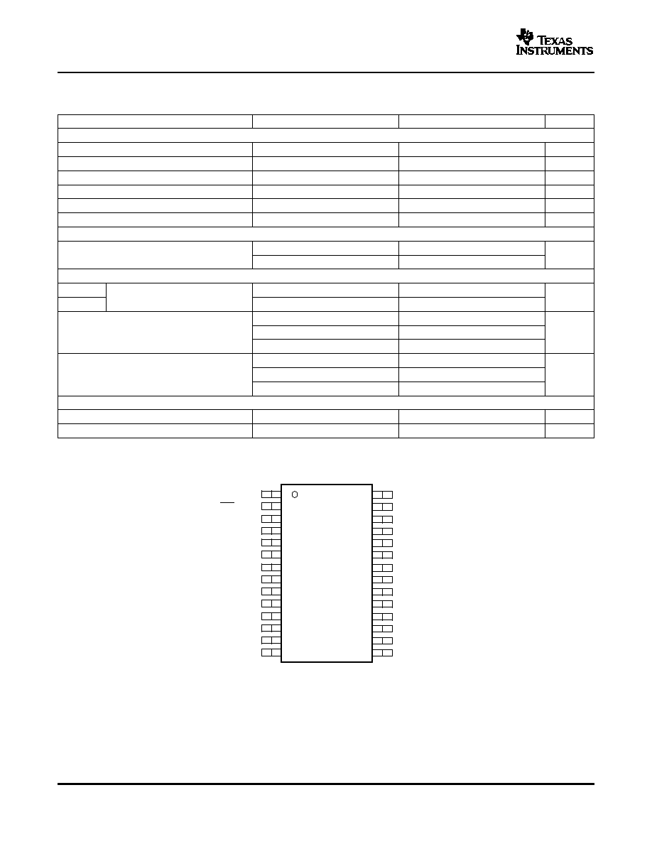
1
2
3
4
5
6
7
8
9
10
11
12
13
14
28
27
26
25
24
23
22
21
20
19
18
17
16
15
ZERO1
MS/ADR
MC/SCL
MD/SDA
SCK
DATA1
BCK
LRCK
V
DD
DGND
DATA2
DATA3
DATA4
MSEL
ZERO2
V
OUT
1
V
OUT
2
V
COM
AGND2
V
CC
2
V
OUT
3
V
OUT
4
V
OUT
5
V
OUT
6
AGND1
V
CC
1
V
OUT
7
V
OUT
8
PCM1680
(TOP VIEW)
P0015-01
PCM1680
SLES133 ş MARCH 2005
ELECTRICAL CHARACTERISTICS (continued)
all specifications at T
A
= 25
░
C, V
CC
= V
DD
= 5 V, f
S
= 48 kHz, system clock = 512 f
S
, and 24-bit data, unless otherwise noted
PARAMETER
TEST CONDITIONS
MIN
TYP
MAX
UNIT
Filter Characteristics (Slow Rolloff)
Pass band
▒
0.5 dB
0.198 f
S
Stop band
0.884 f
S
Pass-band ripple
▒
0.5
dB
Stop-band attenuation
Stop band = 0.884 f
S
ş35
dB
Delay time
20/f
S
De-emphasis error
▒
0.1
dB
ANALOG FILTER PERFORMANCE
at 20 kHz
ş0.02
Frequency response
dB
at 44 kHz
ş0.07
POWER SUPPLY REQUIREMENTS
V
DD
4.75
5
5.25
Voltage range
Vdc
V
CC
4.75
5
5.25
f
S
= 48 kHz
91
110
I
DD
+ I
CC
Supply Current
f
S
= 96 kHz, system clock = 256 f
S
102
mA
f
S
= 192 kHz, system clock = 128 f
S
106
f
S
= 48 kHz
455
605
Power dissipation
f
S
= 96 kHz, system clock = 256 f
S
510
mW
f
S
= 192 kHz, system clock = 128 f
S
530
TEMPERATURE RANGE
Operation temperature
ş25
70
░
C
JA
Thermal resistance
70
░
C/W
4

www.ti.com
PCM1680
SLES133 ş MARCH 2005
TERMINAL FUNCTIONS
TERMINAL
I/O
DESCRIPTION
NAME
NO.
AGND1
18
ş
Analog ground
AGND2
24
ş
Analog ground
BCK
7
I
Shift clock input for serial audio data
(1)
DATA1
6
I
Serial audio data input for V
OUT
1 and V
OUT
2
(1)
DATA2
11
I
Serial audio data input for V
OUT
3 and V
OUT
4
(1)
DATA3
12
I
Serial audio data input for V
OUT
5 and V
OUT
6
(1)
DATA4
13
I
Serial audio data input for V
OUT
7 and V
OUT
8
(1)
DGND
10
ş
Digital ground
LRCK
8
I
Left and right clock input. The frequency of this clock is equal to the sampling rate, f
S
.
(1)
MC/SCL
3
I
Shift clock input for SPI, serial clock input for I
2
C
(1) (2)
MD/SDA
4
I/O
Serial data input for SPI, serial data input/output for I
2
C
(1) (2) (3)
MS/ADR
2
I
Select input for SPI, address input for I
2
C
(1) (4)
MSEL
14
I
I
2
C/SPI select
(1)(4)
SCK
5
I
System clock input. Input frequency is 128, 192, 256, 384, 512, 768, or 1152 f
S
.
(1)
V
CC
1
17
ş
Analog power supply, 5-V
V
CC
2
23
ş
Analog power supply, 5-V
V
COM
25
ş
Common voltage output. This pin should be bypassed with a 10-
Á
F capacitor to AGND.
V
DD
9
ş
Digital power supply, 5-V
V
OUT
1
27
O
Voltage output for audio signal corresponding to L-ch on DATA1
V
OUT
2
26
O
Voltage output for audio signal corresponding to R-ch on DATA1
V
OUT
3
22
O
Voltage output for audio signal corresponding to L-ch on DATA2
V
OUT
4
21
O
Voltage output for audio signal corresponding to R-ch on DATA2
V
OUT
5
20
O
Voltage output for audio signal corresponding to L-ch on DATA3
V
OUT
6
19
O
Voltage output for audio signal corresponding to R-ch on DATA3
V
OUT
7
16
O
Voltage output for audio signal corresponding to L-ch on DATA4
V
OUT
8
15
O
Voltage output for audio signal corresponding to R-ch on DATA4
ZERO1
1
O
Zero-flag output 1
ZERO2
28
O
Zero-flag output 2
(1)
Schmitt-trigger input
(2)
Pulldown in SPI mode
(3)
Open-drain output in I
2
C mode
(4)
Pulldown
5
www.ti.com
Output Amp and
Low-Pass Filter
System Clock
Manager
Enhanced
Multilevel
Delta-Sigma
Modulator
DAC
Serial
Input
I/F
Function
Control
I/F
System Clock
Zero Detect
Power Supply
DAC
Output Amp and
DAC
DAC
Output Amp and
DAC
Output Amp and
DAC
Output Amp and
V
OUT
1
V
OUT
2
V
OUT
3
V
COM
V
OUT
4
V
OUT
5
V
OUT
6
Low-Pass Filter
Low-Pass Filter
Low-Pass Filter
Low-Pass Filter
Low-Pass Filter
Output Amp and
B0033-01
AGND2
V
C
C
2
AGND1
V
C
C
1
DGND
V
D
D
ZERO1
ZERO2
BCK
LRCK
DATA1 (1, 2)
DATA2 (3, 4)
DATA3 (5, 6)
DATA4 (7, 8)
MS/ADR
MC/SCL
MD/SDA
MSEL
SCK
8
y
Oversampling
Digital Filter
With
Function
Controller
DAC
Output Amp and
DAC
Output Amp and
V
OUT
7
V
OUT
8
Low-Pass Filter
Low-Pass Filter
PCM1680
SLES133 ş MARCH 2005
Functional Block Diagram
6
www.ti.com
TYPICAL PERFORMANCE CURVES
DIGITAL FILTER (DE-EMPHASIS OFF)
Frequency [
Î
f
S
]
-0.05
-0.04
-0.03
-0.02
-0.01
0.00
0.01
0.02
0.03
0.04
0.05
0.0
0.1
0.2
0.3
0.4
0.5
Amplitude ş dB
G002
Frequency [
Î
f
S
]
-140
-120
-100
-80
-60
-40
-20
0
0
1
2
3
4
Amplitude ş dB
G001
Frequency [
Î
f
S
]
-140
-120
-100
-80
-60
-40
-20
0
0
1
2
3
4
Amplitude ş dB
G003
Frequency [
Î
f
S
]
-5
-4
-3
-2
-1
0
1
2
3
4
5
0.0
0.1
0.2
0.3
0.4
0.5
Amplitude ş dB
G004
PCM1680
SLES133 ş MARCH 2005
All specifications at T
A
= 25
░
C, V
CC
= 5 V, f
S
= 48 kHz, system clock = 512 f
S
, and 24-bit data, unless otherwise noted
FREQUENCY RESPONSE
PASS-BAND FREQUENCY RESPONSE
(SHARP ROLLOFF)
(SHARP ROLLOFF)
Figure 1.
Figure 2.
FREQUENCY RESPONSE
TRANSITION CHARACTERISTICS
(SLOW ROLLOFF)
(SLOW ROLLOFF)
Figure 3.
Figure 4.
7

www.ti.com
TYPICAL PERFORMANCE CURVES (Continued)
DE-EMPHASIS FILTER
f ş Frequency ş kHz
-0.5
-0.4
-0.3
-0.2
-0.1
0.0
0.1
0.2
0.3
0.4
0.5
0
2
4
6
8
10
12
14
De-Emphasis Error ş dB
f
S
= 32 kHz
G006
-10
-9
-8
-7
-6
-5
-4
-3
-2
-1
0
0
2
4
6
8
10
12
14
f ş Frequency ş kHz
De-Emphasis Level ş dB
f
S
= 32 kHz
G005
f ş Frequency ş kHz
-0.5
-0.4
-0.3
-0.2
-0.1
0.0
0.1
0.2
0.3
0.4
0.5
0
2
4
6
8
10
12
14
16
18
20
De-Emphasis Error ş dB
f
S
= 44.1 kHz
G008
f ş Frequency ş kHz
-10
-9
-8
-7
-6
-5
-4
-3
-2
-1
0
0
2
4
6
8
10
12
14
16
18
20
De-Emphasis Level ş dB
f
S
= 44.1 kHz
G007
PCM1680
SLES133 ş MARCH 2005
All specifications at T
A
= 25
░
C, V
CC
= 5 V, f
S
= 48 kHz, system clock = 512 f
S
, and 24-bit data, unless otherwise noted
DE-EMPHASIS
DE-EMPHASIS ERROR
Figure 5.
Figure 6.
DE-EMPHASIS
DE-EMPHASIS ERROR
Figure 7.
Figure 8.
8
www.ti.com
TYPICAL PERFORMANCE CURVES (Continued)
DE-EMPHASIS FILTER (Continued)
f ş Frequency ş kHz
-0.5
-0.4
-0.3
-0.2
-0.1
0.0
0.1
0.2
0.3
0.4
0.5
0
2
4
6
8
10
12
14
16
18
20
22
De-Emphasis Error ş dB
f
S
= 48 kHz
G010
f ş Frequency ş kHz
-10
-9
-8
-7
-6
-5
-4
-3
-2
-1
0
0
2
4
6
8
10
12
14
16
18
20
22
De-Emphasis Level ş dB
f
S
= 48 kHz
G009
ANALOG FILTER
-70
-60
-50
-40
-30
-20
-10
0
10
f - Frequency - Hz
Amplitude - dB
1
100
1k
10k
G011
10
PCM1680
SLES133 ş MARCH 2005
All specifications at T
A
= 25
░
C, V
CC
= 5 V, f
S
= 48 kHz, system clock = 512 f
S
, and 24-bit data, unless otherwise noted
DE-EMPHASIS
DE-EMPHASIS ERROR
Figure 9.
Figure 10.
ANALOG FILTER PERFORMANCE
Figure 11.
9

www.ti.com
TYPICAL PERFORMANCE CURVES (Continued)
Analog Dynamic Performance
Supply Voltage Characteristics
V
CC
- Supply Voltage - V
4.75
5.00
5.25
THD+N - T
otal Harmonic Distortion + Noise - %
G012
0.001
0.01
V
CC
ş Supply Voltage ş V
96
98
100
102
104
106
108
110
4.75
5.00
5.25
Dynamic Range ş dB
G013
V
CC
ş Supply Voltage ş V
96
98
100
102
104
106
108
110
4.75
5.00
5.25
SNR ş Signal-to-Noise Ratio - dB
G014
V
CC
ş Supply Voltage ş V
96
98
100
102
104
106
108
110
4.75
5.00
5.25
Channel Separation ş dB
G015
PCM1680
SLES133 ş MARCH 2005
All specifications at T
A
= 25
░
C, V
CC
= 5 V, f
S
= 48 kHz, system clock = 512 f
S
, and 24-bit data, unless otherwise noted
TOTAL HARMONIC DISTORTION + NOISE
DYNAMIC RANGE
vs
vs
SUPPLY VOLTAGE
SUPPLY VOLTAGE
Figure 12.
Figure 13.
SIGNAL-TO-NOISE RATIO
CHANNEL SEPARATION
vs
vs
SUPPLY VOLTAGE
SUPPLY VOLTAGE
Figure 14.
Figure 15.
10

www.ti.com
TYPICAL PERFORMANCE CURVES (Continued)
Temperature Characteristics
T
A
- Free-Air Temperature -
░
C
-25
0
25
50
75
THD+N - T
otal Harmonic Distortion + Noise - %
G016
0.001
0.01
T
A
- Free-Air Temperature -
░
C
96
98
100
102
104
106
108
110
-25
0
25
50
75
Dynamic Range ş dB
G017
T
A
- Free-Air Temperature -
░
C
96
98
100
102
104
106
108
110
-25
0
25
50
75
SNR ş Signal-to-Noise Ratio - dB
G018
T
A
- Free-Air Temperature -
░
C
96
98
100
102
104
106
108
110
-25
0
25
50
75
Channel Separation ş dB
G019
PCM1680
SLES133 ş MARCH 2005
All specifications at T
A
= 25
░
C, V
CC
= 5 V, f
S
= 48 kHz, system clock = 512 f
S
, and 24-bit data, unless otherwise noted
TOTAL HARMONIC DISTORTION + NOISE
DYNAMIC RANGE
vs
vs
TEMPERATURE
TEMPERATURE
Figure 16.
Figure 17.
SIGNAL-TO-NOISE RATIO
CHANNEL SEPARATION
vs
vs
TEMPERATURE
TEMPERATURE
Figure 18.
Figure 19.
11
www.ti.com
SYSTEM CLOCK INPUT
t
(SCKH)
System Clock
t
(SCKL)
2 V
0.8 V
H
L
System Clock
Pulse Cycle
Time
(1)
T0005-08
PCM1680
SLES133 ş MARCH 2005
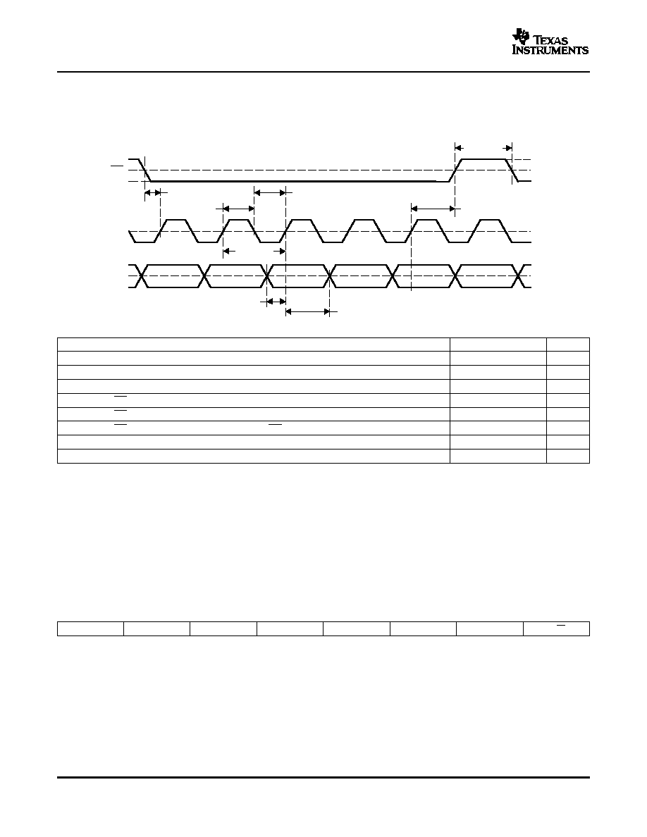
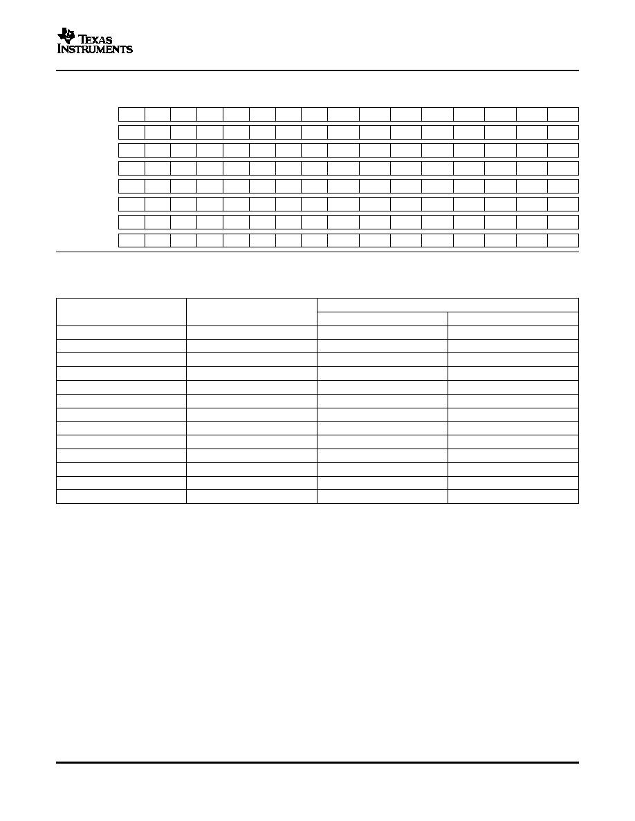
The PCM1680 requires a system clock for operating the digital interpolation filters and multilevel delta-sigma
modulators. The system clock is applied at the SCK (pin 5) input. Table 1 shows examples of system clock
frequencies for common audio sampling rates.
Figure 20 shows the timing requirements for the system clock input. For optimal performance, it is important to
use a clock source with low phase jitter and noise. Texas Instruments' PLL170x multi-clock generator is an
excellent choice for providing the PCM1680 system clock source.
Table 1. System Clock Frequencies for Common Audio Sampling Frequencies
SAMPLING
SYSTEM CLOCK FREQUENCY (f
SCK
), MHz
FREQUENCY
128 f
S
192 f
S
256 f
S
384 f
S
512 f
S
768 f
S
1152 f
S
8 kHz
1.024
1.536
2.048
3.072
4.096
6.144
9.216
16 kHz
2.048
3.072
4.096
6.144
8.192
12.288
18.432
32 kHz
4.096
6.144
8.192
12.288
16.384
24.576
36.864
44.1 kHz
5.6448
8.4672
11.2896
16.9344
22.5792
33.8688
ş
(1)
48 kHz
6.144
9.216
12.288
18.432
24.576
36.864
ş
(1)
88.2 kHz
11.2896
16.9344
22.5792
33.8688
ş
(1)
ş
(1)
ş
(1)
96 kHz
12.288
18.432
24.576
36.864
ş
(1)
ş
(1)
ş
(1)
192 kHz
24.576
36.864
ş
(1)
ş
(1)
ş
(1)
ş
(1)
ş
(1)
(1)
This system clock frequency is not supported for the given sampling frequency.
(1)
1/128 f
S
, 1/192 f
S
, 1/256 f
S
, 1/384 f
S
, 1/512 f
S
, 1/768 f
S
, or 1/1152 f
S
PARAMETER
MIN
MAX
UNIT
t
(SCKH)
System clock pulse duration, HIGH
7
ns
t
(SCKL)
System clock pulse duration, LOW
7
ns
Figure 20. System Clock Timing
12

www.ti.com
POWER-ON-RESET FUNCTION
Reset
Reset Release
V
CC
3.7 V
3 V
2.2 V
Internal Reset
System Clock
T0014-06
0 V
Don't Care
3072 System Clocks
AUDIO SERIAL INTERFACE
PCM1680
SLES133 ş MARCH 2005
The PCM1680 includes a power-on-reset function. Figure 21 shows the operation of this function. With the
system clock active and V
CC
> 3 V (typical, 2.2 V to 3.7 V), the power-on-reset function is enabled. The
initialization sequence requires 3072 system clocks from the time V
CC
> 3 V (typical, 2.2 V to 3.7 V). After the
initialization period, the PCM1680 is set to its reset default state, as described in the Mode Control Register
section of this data sheet.
During the reset period (3072 system clocks), the analog output is forced to the common voltage (V
COM
), or
V
CC
/2. After the reset period, the internal registers are initialized in the next 1/f
S
period and if SCK, BCK, and
LRCK are provided continuously, the PCM1680 provides the proper analog output with group delay
corresponding to the input data.
Figure 21. Power-On-Reset Timing
The audio serial interface for the PCM1680 comprises a 6-wire synchronous serial port. It includes LRCK (pin 8),
BCK (pin 7), and DATA1 (pin 6), DATA2 (pin 11), DATA3 (pin 12), and DATA4 (pin 13). BCK is the serial audio
bit clock, and it is used to clock the serial data present on DATA1, DATA2, DATA3, and DATA4 into the audio
interface serial shift register. Serial data is clocked into the PCM1680 on the rising edge of BCK. LRCK is the
serial audio left/right word clock. It is used to latch serial data into the serial audio interface internal registers.
Both LRCK and BCK must be synchronous with the system clock. Ideally, it is recommended that LRCK and
BCK are derived from the system clock input, SCK. LRCK is operated at the sampling frequency, f
S
. BCK can be
operated at 32, 48, or 64 times the sampling frequency.
Internal operation of the PCM1680 is synchronized with LRCK. Accordingly, internal operation is suspended
when the sampling rate clock, LRCK, is changed or when SCK and/or BCK is interrupted at least for a 3-bit clock
cycle. If SCK, BCK, and LRCK are provided continuously after this suspended condition, the internal operation is
resynchronized automatically within the following 3/f
S
period. External resetting is not required.
13
www.ti.com
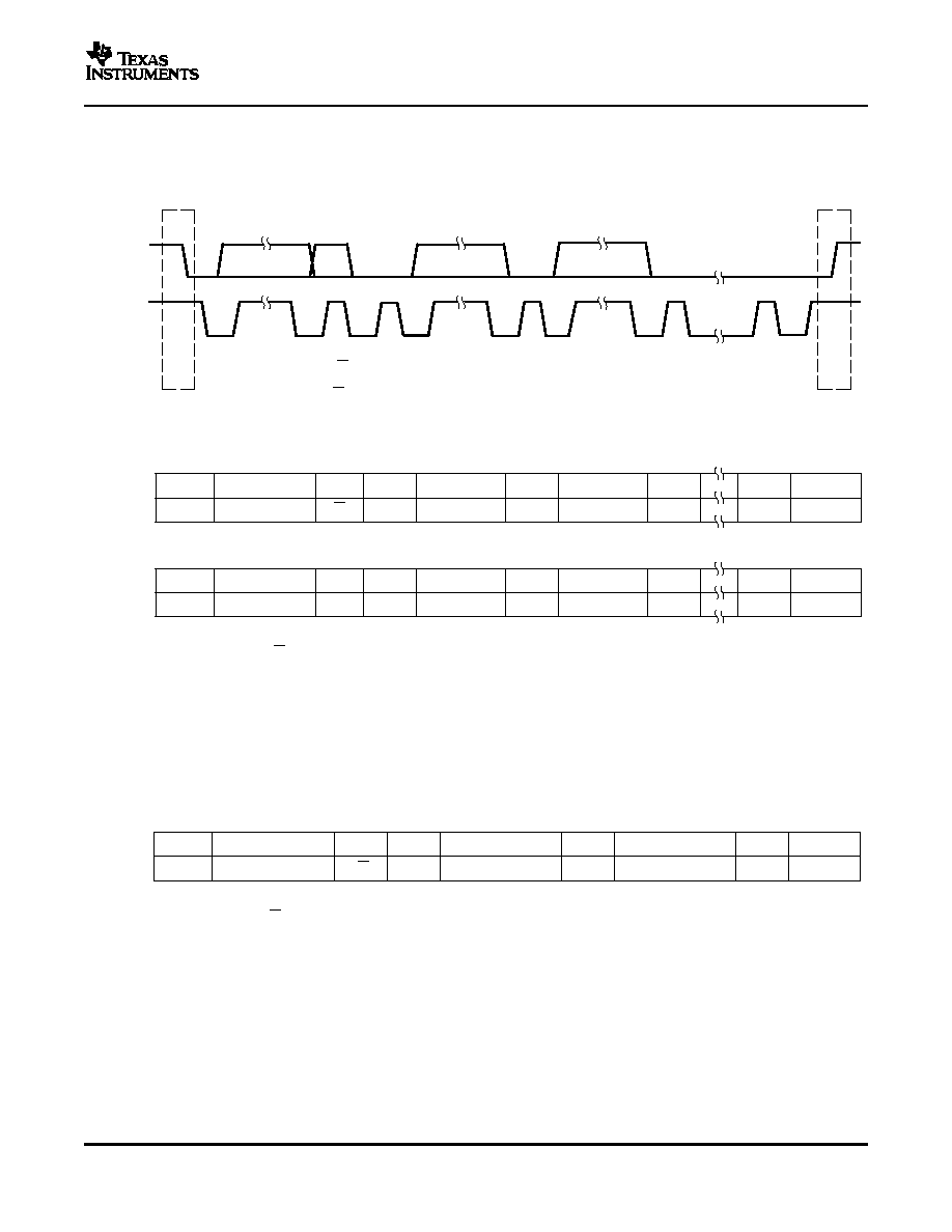
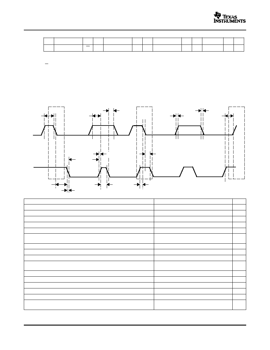
AUDIO DATA FORMATS AND TIMING
PCM1680
SLES133 ş MARCH 2005
The PCM1680 supports industry-standard audio data formats, including right-justified, I
2
S, and left-justified. The
data formats are shown in Figure 22. Data formats are selected using the format bits, FMT[2:0], located in control
register 9 of the PCM1680. The default data format is 24-bit left-justified. All formats require binary 2s
complement, MSB-first audio data. Figure 23 shows a detailed timing diagram for the serial audio interface.
DATA1, DATA2, DATA3, and DATA4 each carry two audio channels, designated as the left and right channels.
The left-channel data always precedes the right-channel data in the serial data stream for all data formats.
Table 2 shows the mapping of the digital input data to the analog output pins.
Table 2. Audio Input Data to Analog Output Mapping
DATA INPUT
CHANNEL
ANALOG OUTPUT
Left
V
OUT
1
DATA1
Right
V
OUT
2
Left
V
OUT
3
DATA2
Right
V
OUT
4
Left
V
OUT
5
DATA3
Right
V
OUT
6
Left
V
OUT
7
DATA4
Right
V
OUT
8
14

www.ti.com
LRCK
(2) I
2
S Data Format; L-Channel = LOW, R-Channel = HIGH
MSB
LSB
1/f
S
(= 32 f
S
, 48 f
S,
or 64 f
S
)
18-Bit Right-Justified, BCK = 48 f
S
or 64 f
S
1/f
S
(1) Right-Justified Data Format; L-Channel = HIGH, R-Channel = LOW
(3) Left-Justified Data Format; L-Channel = HIGH, R-Channel = LOW
MSB
LSB
20-Bit Right-Justified, BCK = 48 f
S
or 64 f
S
MSB
LSB
24-Bit Right-Justified, BCK = 48 f
S
or 64 f
S
1/f
S
(= 32 f
S
, 48 f
S
or 64 f
S
)
(= 32 f
S
, 48 f
S,
or 64 f
S
)
LSB
16-Bit Right-Justified, BCK = 48 f
S
or 64 f
S
16-Bit Right-Justified, BCK = 32 f
S
LSB
L-Channel
R-Channel
BCK
DATA
14 15 16
14 15 16
14 15 16
14 15 16
16 17 18
DATA
DATA
DATA
DATA
1
2
3
16 17 18
18 19 20
1
2
3
18 19 20
22 23 24
1
2
3
MSB
LSB
MSB
LSB
LSB
MSB
LSB
1
2
3
14 15 16
14 15 16
1
2
3
16 17 18
1
2
3
18 19 20
22 23 24
MSB
LSB
1
2
3
22 23 24
L-Channel
R-Channel
LRCK
BCK
DATA
1
2
3
1
2
MSB
Nş2
N
Nş1
LSB
1
2
3
MSB
Nş2
N
Nş1
LSB
L-Channel
R-Channel
LRCK
BCK
DATA
1
2
3
Nş2
N
Nş1
1
2
3
Nş2
N
Nş1
1
2
MSB
LSB
LSB
MSB
T0009-02
MSB
1
2
3
MSB
1
2
3
MSB
1
2
3
PCM1680
SLES133 ş MARCH 2005
Figure 22. Audio Data Input Formats
15

www.ti.com
DATA1, DATA2,
DATA3, DATA4
t
(BCH)
1.4 V
1.4 V
1.4 V
BCK
LRCK
t
(BCL)
t
(LS)
t
(BCY)
t
(LH)
t
(DS)
t
(DH)
T0010-04
OVERSAMPLING RATE CONTROL
ZERO FLAG
PCM1680
SLES133 ş MARCH 2005
PARAMETER
MIN
UNIT
t
(BCY)
BCK pulse cycle time
1/(32 f
S
), 1/(48 f
S
), 1/(64 f
S
)
(1)
t
(BCH)
BCK pulse duration, HIGH
35
ns
t
(BCL)
BCK pulse duration, LOW
35
ns
t
(LS)
LRCK setup time to BCK rising edge
10
ns
t
(LH)
LRCK hold time to BCK rising edge
10
ns
t
(DS)
DATA1, DATA2, DATA3, DATA4 setup time
10
ns
t
(DH)
DATA1, DATA2, DATA3, DATA4 hold time
10
ns
(1)
f
S
is the sampling frequency.
Figure 23. Audio Interface Timing
The PCM1680 automatically controls the oversampling rate of the delta-sigma D/A converters using the system
clock frequency. The oversampling rate is set to 64
Î
oversampling with an 1152-f
S
, 768-f
S
, or 512-f
S
system
clock; 32
Î
oversampling with a 384-f
S
or 256-f
S
system clock; and 16
Î
oversampling with a 192-f
S
or 128-f
S
system clock.
The PCM1680 has two zero-flag pins, ZERO1 (pin 1) and ZERO2 (pin 28), which are assigned to the
combinations A through D as shown in Table 3. Zero-flag combinations are selected using the zero-flag
combination bits, AZRO[1:0], located in control register 13 of the PCM1680. If the input data of the L-channel
and/or R-channel of all assigned channels remains at a logic-0 level for 1024 sampling periods (LRCK clock
periods), ZERO1 and ZERO2 are set to a logic-1 state, or high level. If the input data of any of the assigned
channels contains a logic-1, ZERO1 and ZERO2 are set to a logic-0 state immediately.
The active polarity of the zero-flag output can be inverted by setting the ZREV bit of control register 10 to 1. The
reset default is active-high output or ZREV = 0.
Table 3. Zero-Flag Output Combinations
ZERO-FLAG COMBINATION
ZERO1 (PIN 1)
ZERO2 (PIN 28)
A
DATA1 L-ch
DATA1 R-ch
B
N/A
DATA[1:4]
C
DATA4
DATA[1:3]
D
DATA1
DATA[2:4]
16
www.ti.com
MODE CONTROL
SPI CONTROL INTERFACE
REGISTER WRITE OPERATION
MSB
0
IDX6
IDX5
IDX4
IDX3
IDX2
IDX1
IDX0
D7
D6
D5
D4
D3
D2
D1
D0
0
0
LSB
Register Index (or Address)
Register Data
R0001-01
IDX0
D7
D6
D4
D5
D3
D2
D1
D0
0
MS
MC
MD
X
0
IDX6
X
IDX1
IDX2
IDX3
IDX4
IDX5
IDX6
X
T0048-01
PCM1680
SLES133 ş MARCH 2005
The PCM1680 has many programmable functions which can be controlled in the software control mode. The
functions are controlled by programming and reading the internal registers using the SPI or I
2
C interface. These
two interfaces for mode control can be selected by MSEL (pin 14). The functions of pins 2, 3, and 4 are changed
by MSEL selection as shown in Table 4.
Table 4. Interface Mode Control
PIN FUNCTION
MSEL
INTERFACE MODE
PIN 2
PIN 3
PIN 4
LOW
SPI
MS
MC
MD
HIGH
I
2
C
ADR
SCL
SCA
The SPI control interface of the PCM1680 is a 3-wire synchronous serial port that operates asynchronously to
the serial audio interface. The SPI control interface is used to program the on-chip mode registers. The control
interface includes MD (pin 4), MC (pin 3), and MS (pin 2). MD is the serial data input, used to program the mode
registers. MC is the control port for the serial bit clock, used to shift in the serial data, and MS is the control port
for mode control select, which is used to enable the mode control.
All write operations for the serial control port use 16-bit data words. Figure 24 shows the control data word
format. The most significant bit is a fixed 0 for the write operation. Seven bits, labeled IDX[6:0], set the register
index (or address) for the write operation. The least significant eight bits, D[7:0], contain the data to be written to
the register specified by IDX[6:0].
Figure 25 shows the functional timing diagram for writing to the serial control port. MS is held at a logic-1 state
until a register needs to be written. To start the register write cycle, MS is set to logic-0. Sixteen clock cycles are
then provided on MC, corresponding to the 16 bits of the control data word on MD. After the completion of the
sixteenth clock cycle, MS is set to logic-1 to latch the data into the indexed mode control register.
Figure 24. Control Data Word Format for MD
Figure 25. Write Operation Timing
17
www.ti.com
INTERFACE TIMING REQUIREMENTS
t
(MCH)
MS
t
(MSS)
LSB
t
(MCL)
t
(MHH)
t
(MSH)
t
(MCY)
t
(MDH)
t
(MDS)
MC
MD
T0013-03
I
2
C INTERFACE
SLAVE ADDRESS
PCM1680
SLES133 ş MARCH 2005
Figure 26 shows a detailed timing diagram for the serial control interface. Special attention to the setup and hold
times is required. Also, t
(MSS)
and t
(MSH)
, which define minimum delays between edges of the MS and MC clocks,
require special attention. These timing parameters are critical for proper control port operation.
PARAMETER
MIN
UNIT
t
(MCY)
MC pulse cycle time
100
ns
t
(MCL)
MC pulse duration, LOW
50
ns
t
(MCH)
MC pulse duration, HIGH
50
ns
t
(MHH)
MS pulse duration, HIGH
(1)
ns
t
(MSS)
MS falling edge to MC rising edge
20
ns
t
(MSH)
MS hold time, MC rising edge for LSB to MS rising edge
20
ns
t
(MDH)
MD hold time
15
ns
t
(MDS)
MD setup time
20
ns
(1)
3/(256 f
S
) s (minimum), f
S
: sampling rate
Figure 26. Interface Timing
The PCM1680 supports the I
2
C serial bus and the data transmission protocol for standard mode as a slave
device. This protocol is explained in the I
2
C specification 2.0. The PCM1680 does not support a board-to-board
interface. Figure 27 shows the I
2
C framework for basic read and write operations.
MSB
LSB
1
0
0
1
1
0
ADR
R/W
The PCM1680 has seven bits for its own slave address. The first six bits (MSBs) of the slave address are factory
preset to 1001 10. The next bit of the address byte is the device select bit, which can be user-defined using the
ADR terminal. A maximum of two PCM1680s can be connected on the same bus at one time. Each PCM1680
responds when it receives its own slave address.
18
www.ti.com
PACKET PROTOCOL
9
SDA
SCL
St
Start
1-7
8
1-8
9
1-8
9
9
Sp
Stop
Slave Address
ACK
DATA
ACK
DATA
ACK
ACK
Condition
Condition
R/W
Read Operation
Transmitter
M
M
M
S
S
M
S
M
M
M
Data Type
St
Slave Address
R
ACK
DATA
ACK
DATA
ACK
NACK
Sp
Write Operation
Transmitter
M
M
M
S
M
S
M
S
S
M
Data Type
St
Slave Address
W
ACK
DATA
ACK
DATA
ACK
ACK
Sp
R/W:
Read Operation if 1; Otherwise, Write Operation
ACK: Acknowledgement of a Byte if 0
DATA: 8 Bits (Byte)
NACK: Not Acknowledgement if 1
T0049-01
M: Master Device S: Slave Device St: Start Condition
Sp: Stop Condition W: Write R: Read
WRITE OPERATION
Transmitter
M
M
Data Type
Slave Address
Reg Address
Write Data
R0002-01
M: Master Device S: Slave Device
St: Start Condition W: Write ACK: Acknowledge Sp: Stop Condition
M
M
S
M
St
W
ACK
Sp
S
ACK
M
S
ACK
READ OPERATION
PCM1680
SLES133 ş MARCH 2005
A master device must control packet protocol, which consists of start condition, slave address, read/write bit,
data if writing or acknowledge if reading, and stop condition. The PCM1680 supports only slave receivers and
slave transmitters.
Figure 27. Basic I
2
C Framework
A master can write to any PCM1680 registers using a single access. The master sends a PCM1680 slave
address with a write bit, a register address, and the data. When undefined registers are accessed, the PCM1680
sends an acknowledgement, but the write operation does not occur. Figure 28 is a diagram of the write
operation.
Figure 28. Write Operation
A master can read any PCM1680 register using a single access. The master sends a PCM1680 slave address
with a read bit after transferring the register address. Then the PCM1680 transfers the data in the register
specified. Figure 29 is a diagram of the read operation.
19
www.ti.com
R0002-02
M: Master Device S: Slave Device St: Start Condition
Sr: Repeated Start Condition ACK: Acknowledge Sp: Stop Condition NACK: Not Acknowledge
W: Write R: Read
Transmitter
M
M
M
S
Data Type
St
Slave Address
W
ACK
M
Reg Address
M
Sr
M
Slave Address
S
ACK
M
R
S
ACK
M
Sp
M
NACK
S
Data
TIMING DIAGRAM
SDA
SCL
t
(BUF)
t
(D-SU)
t
(D-HD)
Start
t
(LOW)
t
(S-HD)
t
(SCL-F)
t
(SCL-R)
t
(HI)
Repeated Start
t
(RS-SU)
t
(RS-HD)
t
(SDA-F)
t
(SDA-R)
t
(P-SU)
Stop
T0050-01
PCM1680
SLES133 ş MARCH 2005
NOTE: The slave address after the repeated start condition must be the same as the previous slave address.
Figure 29. Read Operation
PARAMETER
MIN
MAX
UNIT
f
(SCL)
SCL clock frequency
100
kHz
t
(BUF)
Bus free time between a STOP and START condition
4.7
Á
s
t
(LOW)
Low period of the SCL clock
4.7
Á
s
t
(HI)
High period of the SCL clock
4
Á
s
t
(RS-SU)
Setup time for (repeated) START condition
4.7
Á
s
t
(S-HD)
Hold time for (repeated) START condition
4
Á
s
t
(RS-HD)
t
(D-SU)
Data setup time
250
ns
t
(D-HD)
Data hold time
0
900
ns
t
(SCL-R)
Rise time of SCL signal
20 + 0.1 C
B
1000
ns
t
(SCL-R1)
Rise time of SCL signal after a repeated START condition and after
20 + 0.1 C
B
1000
ns
an acknowledge bit
t
(SCL-F)
Fall time of SCL signal
20 + 0.1 C
B
1000
ns
t
(SDA-R)
Rise time of SDA signal
20 + 0.1 C
B
1000
ns
t
(SDA-F)
Fall time of SDA signal
20 + 0.1 C
B
1000
ns
t
(P-SU)
Setup time for STOP condition
4
Á
s
C
B
Capacitive load for SDA and SCL lines
400
pF
V
NH
Noise margin at high level for each connected device (including
0.2 V
DD
V
hysteresis)
Figure 30. Interface Timing
20
www.ti.com
MODE CONTROL REGISTERS
USER-PROGRAMMABLE MODE CONTROLS
REGISTER MAP
RESERVED REGISTERS
PCM1680
SLES133 ş MARCH 2005
The PCM1680 includes a number of user-programmable functions which are accessed via control registers. The
registers are programmed using the serial control interface which is discussed in the Mode Control section of this
data sheet. Table 5 lists the available mode control functions, along with their reset default conditions and
associated register index.
The mode control register map is shown in Table 6. The MSB of all registers is fixed to 0. Each register also
includes an index (or address) indicated by the IDX[6:0] bits.
Registers 0, 11, and 15 are reserved for factory use. To ensure proper operation, the user should not write to
these registers.
Table 5. User-Programmable Mode Controls
FUNCTION
RESET DEFAULT
REGISTER
BIT
Digital attenuation control, 0 dB to ş63 dB 0 dB, no attenuation
1ş6, 16, 17
AT1[7:0], AT2[7:0], AT3[7:0], AT4[7:0],
in 0.5-dB steps
AT5[7:0], AT6[7:0], AT7[7:0], AT8[7:0]
Soft mute control
Mute disabled
7, 18
MUT[6:1], MUT[8:7]
DAC1şDAC8 operation control
DAC1şDAC8 enabled
8, 19
DAC[6:1], DAC[8:7]
Audio data format control
24-bit, left-justified
9
FMT[2:0]
Digital filter rolloff control
Sharp rolloff
9
FLT
De-emphasis all-channel function control
De-emphasis of all channels
10
DMC
disabled
De-emphasis all-channel sample rate
44.1 kHz
10
DMF[1:0]
selection
Output phase select
Normal phase
10
DREV
Zero-flag polarity select
High
10
ZREV
Software reset control
Reset disabled
10
SRST
Oversampling rate control
Î
64,
Î
32,
Î
16
12
OVER
Zero-flag combination select
ZERO1: DATA1 Lch
13
AZRO[1:0]
ZERO2: DATA1 Rch
Digital attenuation mode select
0 to ş63 dB, 0.5-dB step
13
DAMS
Zero-detect status (read-only, I
2
C
N/A
14
ZERO[8:1]
interface only)
21

www.ti.com
PCM1680
SLES133 ş MARCH 2005
Table 6. Mode Control Register Map
IDX
REGIS-
B15
B14
B13
B12
B11
B10
B9
B8
B7
B6
B5
B4
B3
B2
B1
B0
(B8şB14)
TER
01h
1
0
IDX6
IDX5
IDX4
IDX3
IDX2
IDX1
IDX0
AT17
AT16
AT15
AT14
AT13
AT12
AT11
AT10
02h
2
0
IDX6
IDX5
IDX4
IDX3
IDX2
IDX1
IDX0
AT27
AT26
AT25
AT24
AT23
AT22
AT21
AT20
03h
3
0
IDX6
IDX5
IDX4
IDX3
IDX2
IDX1
IDX0
AT37
AT36
AT35
AT34
AT33
AT32
AT31
AT30
04h
4
0
IDX6
IDX5
IDX4
IDX3
IDX2
IDX1
IDX0
AT47
AT46
AT45
AT44
AT43
AT42
AT41
AT40
05h
5
0
IDX6
IDX5
IDX4
IDX3
IDX2
IDX1
IDX0
AT57
AT56
AT55
AT54
AT53
AT52
AT51
AT50
06h
6
0
IDX6
IDX5
IDX4
IDX3
IDX2
IDX1
IDX0
AT67
AT66
AT65
AT64
AT63
AT62
AT61
AT60
07h
7
0
IDX6
IDX5
IDX4
IDX3
IDX2
IDX1
IDX0
RSV
(1)
RSV
(1)
MUT6
MUT5
MUT4
MUT3
MUT2
MUT1
08h
8
0
IDX6
IDX5
IDX4
IDX3
IDX2
IDX1
IDX0
RSV
(1)
RSV
(1)
DAC6
DAC5
DAC4
DAC3
DAC2
DAC1
09h
9
0
IDX6
IDX5
IDX4
IDX3
IDX2
IDX1
IDX0
RSV
(1)
RSV
(1)
FLT
RSV
(1)
RSV
(1)
FMT2
FMT1
FMT0
0Ah
10
0
IDX6
IDX5
IDX4
IDX3
IDX2
IDX1
IDX0
SRST
ZREV
DREV
DMF1
DMF0
RSV
(1)
RSV
(1)
DMC
0Ch
12
0
IDX6
IDX5
IDX4
IDX3
IDX2
IDX1
IDX0
OVER
RSV
(1)
RSV
(1)
RSV
(1)
RSV
(1)
RSV
(1)
RSV
(1)
RSV
(1)
0Dh
13
0
IDX6
IDX5
IDX4
IDX3
IDX2
IDX1
IDX0
DAMS
AZRO1 AZRO0
RSV
(1)
RSV
(1)
RSV
(1)
RSV
(1)
RSV
(1)
0Eh
14
0
IDX6
IDX5
IDX4
IDX3
IDX2
IDX1
IDX0
ZERO8 ZERO7 ZERO6 ZERO5 ZERO4 ZERO3 ZERO2 ZERO1
10h
16
0
IDX6
IDX5
IDX4
IDX3
IDX2
IDX1
IDX0
AT77
AT76
AT75
AT74
AT73
AT72
AT71
AT70
11h
17
0
IDX6
IDX5
IDX4
IDX3
IDX2
IDX1
IDX0
AT87
AT86
AT85
AT84
AT83
AT82
AT81
AT80
12h
18
0
IDX6
IDX5
IDX4
IDX3
IDX2
IDX1
IDX0
RSV
(1)
RSV
(1)
RSV
(1)
RSV
(1)
RSV
(1)
RSV
(1)
MUT8
MUT7
13h
19
0
IDX6
IDX5
IDX4
IDX3
IDX2
IDX1
IDX0
RSV
(1)
RSV
(1)
RSV
(1)
RSV
(1)
RSV
(1)
RSV
(1)
DAC8
DAC7
(1)
Reserved for test operation. It should be set to 0 during normal operation.
22
www.ti.com
REGISTER DEFINITIONS
ATx[7:0]: Digital Attenuation Level Setting
PCM1680
SLES133 ş MARCH 2005
B15
B14
B13
B12
B11
B10
B9
B8
B7
B6
B5
B4
B3
B2
B1
B0
REGISTER 1
0
IDX6
IDX5
IDX4
IDX3
IDX2
IDX1
IDX0
AT17
AT16
AT15
AT14
AT13
AT12
AT11
AT10
REGISTER 2
0
IDX6
IDX5
IDX4
IDX3
IDX2
IDX1
IDX0
AT27
AT26
AT25
AT24
AT23
AT22
AT21
AT20
REGISTER 3
0
IDX6
IDX5
IDX4
IDX3
IDX2
IDX1
IDX0
AT37
AT36
AT35
AT34
AT33
AT32
AT31
AT30
REGISTER 4
0
IDX6
IDX5
IDX4
IDX3
IDX2
IDX1
IDX0
AT47
AT46
AT45
AT44
AT43
AT42
AT41
AT40
REGISTER 5
0
IDX6
IDX5
IDX4
IDX3
IDX2
IDX1
IDX0
AT57
AT56
AT55
AT54
AT53
AT52
AT51
AT50
REGISTER 6
0
IDX6
IDX5
IDX4
IDX3
IDX2
IDX1
IDX0
AT67
AT66
AT65
AT64
AT63
AT62
AT61
AT60
REGISTER 16
0
IDX6
IDX5
IDX4
IDX3
IDX2
IDX1
IDX0
AT77
AT76
AT75
AT74
AT73
AT72
AT711
AT70
REGISTER 17
0
IDX6
IDX5
IDX4
IDX3
IDX2
IDX1
IDX0
AT87
AT86
AT85
AT84
AT83
AT82
AT81
AT80
where x = 1ş8, corresponding to the DAC output V
OUT
x. Default value: 1111 1111b
ATx[7:0]
DECIMAL VALUE
ATTENUATION LEVEL SETTING
DAMS = 0
DAMS = 1
1111 1111b
255
0 dB, no attenuation (default)
0 dB, no attenuation (default)
1111 1110b
254
ş0.5 dB
ş1 dB
1111 1101b
253
ş1 dB
ş2 dB
:
:
:
:
1001 1100b
156
ş49.5 dB
ş99 dB
1001 1011b
155
ş50 dB
ş100 dB
1001 1010b
154
ş50.5 dB
Mute
:
:
:
:
1000 0010b
130
ş62.5 dB
Mute
1000 0001b
129
ş63 dB
Mute
1000 0000b
128
Mute
Mute
:
:
:
:
0000 0000b
0
Mute
Mute
Each DAC output, V
OUT
1 through V
OUT
8, has a digital attenuation function. The attenuation level can be set from
0 dB to R dB, in S-dB steps. Changes in attenuation levels are made by incrementing or decrementing by one
step (S-dB) for every 8/f
S
time interval until the programmed attenuation setting is reached. Alternatively, the
attenuation level can be set to infinite attenuation (or mute). Range (R) and step (S) are ş63 and 0.5,
respectively, for DAMS = 0 and ş100 and 1, respectively, for DAMS = 1. The DAMS bit is defined in register 13.
The attenuation data for each channel can be set individually. The attenuation level can be calculated using the
following formula:
Attenuation level (dB) = S
Ě
(ATx[7:0]
DEC
ş 255)
where ATx[7:0]
DEC
= 0 through 255. For ATx[7:0]
DEC
= 0 through 128 with DAMS = 0 or for ATx[7:0]
DEC
= 0
through 154 with DAMS = 1, the attenuation is set to infinite attenuation (mute).
23

www.ti.com
MUTx: Soft Mute Control
DACx: DAC Operation Control
PCM1680
SLES133 ş MARCH 2005
B15
B14
B13
B12
B11
B10
B9
B8
B7
B6
B5
B4
B3
B2
B1
B0
REGISTER 7
0
IDX6
IDX5
IDX4
IDX3
IDX2
IDX1
IDX0
RSV
RSV
MUT6
MUT5
MUT4
MUT3
MUT2
MUT1
REGISTER 18
0
IDX6
IDX5
IDX4
IDX3
IDX2
IDX1
IDX0
RSV
RSV
RSV
RSV
RSV
RSV
MUT8
MUT7
where x = 1ş8, corresponding to the DAC output V
OUT
x. Default value: 0
MUTx = 0
Mute disabled (default)
MUTx = 1
Mute enabled
The mute bits, MUT1 through MUT8, are used to enable or disable the soft mute function for the corresponding
DAC outputs, V
OUT
1 through V
OUT
8. The soft mute function is incorporated into the digital attenuators. When
mute is disabled (MUTx = 0), the attenuator and DAC operate normally. When mute is enabled by setting
MUTx = 1, the digital attenuator for the corresponding output is decreased from the current setting to the
infinite-attenuation setting one attenuator step (S-dB) at a time. This provides a quiet, pop-free muting of the
DAC output. On returning from soft mute, by setting MUTx = 0, the attenuator is increased one step at a time to
the previously programmed attenuator level. The step size, S, is 0.5 dB for DAMS = 0 and 1 dB for DAMS = 1.
B15
B14
B13
B12
B11
B10
B9
B8
B7
B6
B5
B4
B3
B2
B1
B0
REGISTER 8
0
IDX6
IDX5
IDX4
IDX3
IDX2
IDX1
IDX0
RSV
RSV
DAC6
DAC5
DAC4
DAC3
DAC2
DAC1
REGISTER 19
0
IDX6
IDX5
IDX4
IDX3
IDX2
IDX1
IDX0
RSV
RSV
RSV
RSV
RSV
RSV
DAC8
DAC7
where x = 1ş8, corresponding to the DAC output V
OUT
x. Default value: 0
DACx = 0
DAC operation enabled (default)
DACx = 1
DAC operation disabled
The DAC operation controls are used to enable and disable the DAC outputs, V
OUT
1 through V
OUT
8. When
DACx = 0, the output amplifier input is connected to the DAC output. When DACx = 1, the output amplifier input
is switched to the dc common voltage (V
COM
), equal to V
CC
/2.
24
www.ti.com
FLT: Digital Filter Rolloff Control
FMT[2:0]: Audio Interface Data Format
SRST: Reset
ZREV: Zero-Flag Polarity Select
PCM1680
SLES133 ş MARCH 2005
B15
B14
B13
B12
B11
B10
B9
B8
B7
B6
B5
B4
B3
B2
B1
B0
REGISTER 9
0
IDX6
IDX5
IDX4
IDX3
IDX2
IDX1
IDX0
RSV
RSV
FLT
RSV
RSV
FMT2
FMT1
FMT0
Default value: 0
FLT = 0
Sharp rolloff (default)
FLT = 1
Slow rolloff
The FLT bit allows users to select the digital filter rolloff that is best suited to their application. Two filter rolloff
selections are available: sharp or slow. The filter responses for these selections are shown in the Typical
Performance Curves section of this data sheet.
Default value: 101b
FMT[2:0]
Audio Data Format Selection
000
24-bit right-justified format, standard data
001
20-bit right-justified format, standard data
010
18-bit right-justified format, standard data
011
16-bit right-justified format, standard data
100
I
2
S format, 16- to 24-bit
101
Left-justified format, 16- to 24-bit (default)
110
Reserved
111
Reserved
The FMT[2:0] bits are used to select the data format for the serial audio interface.
B15
B14
B13
B12
B11
B10
B9
B8
B7
B6
B5
B4
B3
B2
B1
B0
REGISTER 10
0
IDX6
IDX5
IDX4
IDX3
IDX2
IDX1
IDX0
SRST
ZREV
DREV
DMF1
DMF0
RSV
RSV
DMC
Default value: 0
SRST = 0
Reset disabled (default)
SRST = 1
Reset enabled
The SRST bit is used to enable or disable the soft reset function. The operation is the same as the
power-on-reset function with the exception of the reset period, which is 1024 system clocks for the SRST
function. All registers are initialized.
Default value: 0
ZREV = 0
Zero-flag pins high at a zero detect (default)
ZREV = 1
Zero-flag pins low at a zero detect
The ZREV bit allows the user to select the polarity of the zero-flag pins.
25

www.ti.com
DREV: Output Phase Select
DMF[1:0]: Sampling Frequency Selection for the De-Emphasis Function
DMC: Digital De-Emphasis All-Channel Function Control
OVER: Oversampling Rate Control
PCM1680
SLES133 ş MARCH 2005
Default value: 0
DREV = 0
Normal output (default)
DREV = 1
Inverted output
The DREV bit is the output analog signal phase control.
Default value: 00b
DMF[1:0] De-Emphasis Sampling Rate Selection
00
44.1 kHz (default)
01
48 kHz
10
32 kHz
11
Reserved
The DMF[1:0] bits select the sampling frequency used for the digital de-emphasis function when it is enabled.
The de-emphasis curves are shown in the Typical Performance Curves section of this data sheet. The preceding
table shows the available sampling frequencies.
Default value: 0
DMC = 0
De-emphasis disabled for all channels (default)
DMC = 1
De-emphasis enabled for all channels
The DMC bit is used to enable or disable the de-emphasis function for all channels.
B15
B14
B13
B12
B11
B10
B9
B8
B7
B6
B5
B4
B3
B2
B1
B0
REGISTER 12
0
IDX6
IDX5
IDX4
IDX3
IDX2
IDX1
IDX0
OVER
RSV
RSV
RSV
RSV
RSV
RSV
RSV
Default value: 0
System clock frequency = 512 f
S
, 768 f
S
, or 1152 f
S
OVER = 0
Î
64 oversampling (default)
OVER = 1
Î
128 oversampling (applicable only if sampling clock frequency
24 kHz)
System clock frequency = 256 f
S
or 384 f
S
OVER = 0
Î
32 oversampling (default)
OVER = 1
Î
64 oversampling (applicable only if sampling clock frequency
48 kHz)
System clock frequency = 128 f
S
or 192 f
S
OVER = 0
Î
16 oversampling (default)
OVER = 1
Î
32 oversampling (applicable only if sampling clock frequency
96 kHz)
The OVER bit is used to control the oversampling rate of the delta-sigma D/A converters.
Setting OVER = 1 is recommended under the following conditions:
Ě
System clock frequency = 512 f
S
, 768 f
S
, or 1152 f
S
and sampling clock frequency
24 kHz
Ě
System clock frequency = 256 f
S
or 384 f
S
and sampling clock frequency
48 kHz
Ě
System clock frequency = 128 f
S
or 192 f
S
and sampling clock frequency
96 kHz
26
www.ti.com
DAMS: Digital Attenuation Mode Select
AZRO[1:0]: Zero-Flag Channel-Combination Select
ZERO[8:1]: Zero-Detect Status (Read-Only, I
2
C Interface Only)
PCM1680
SLES133 ş MARCH 2005
B15
B14
B13
B12
B11
B10
B9
B8
B7
B6
B5
B4
B3
B2
B1
B0
REGISTER 13
0
IDX6
IDX5
IDX4
IDX3
IDX2
IDX1
IDX0
DAMS
AZRO1
AZRO0
RSV
RSV
RSV
RSV
RSV
Default value: 0
DAMS = 0
Fine step, 0.5 dB/step for 0 to ş63 dB range (default)
DAMS = 1
Wide range, 1 dB/step for 0 to ş100 dB range
The DAMS bit is used to select the digital attenuation mode.
Default value: 00b
AZRO[1:0]
Zero-Flag Channel-Combination Select
00
Combination A (ZERO1: DATA1 L-ch, ZERO2: DATA1 R-ch) (default)
01
Combination B (ZERO1: N/A, ZERO2: DATA1şDATA4)
10
Combination C (ZERO1: DATA4, ZERO2: DATA1şDATA3)
11
Combination D (ZERO1: DATA1, ZERO2: DATA2şDATA4)
The AZRO[1:0] bits are used to select the zero-flag channel combinations for ZERO1 and ZERO2.
B15
B14
B13
B12
B11
B10
B9
B8
B7
B6
B5
B4
B3
B2
B1
B0
REGISTER 14
0
IDX6 IDX5 IDX4 IDX3 IDX2 IDX1 IDX0
ZERO8
ZERO7
ZERO6
ZERO5
ZERO4
ZERO3
ZERO2
ZERO1
Default value: N/A
The ZERO[8:1] bits show the status of zero detect for each channel. The status is set to 1 by detecting a zero
state without regard to the ZREV bit setting.
27
www.ti.com
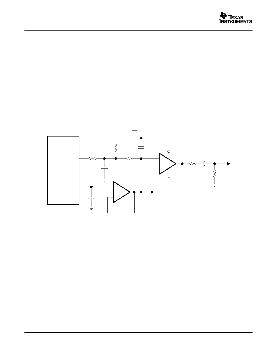
ANALOG OUTPUTS
V
COM
OUTPUT
ş
V
OUT
X
+
PCM1680
A
V
+ *
R
2
R
1
V
COM
OPA2134
+
V
CC
2
3
1
C
1
R
3
R
2
C
2
R
1
C
3
10
Á
F
+
S0056-01
R
4
R
5
+
OPA337
-
To Additional
Low-Pass
Filter Circuits
PCM1680
SLES133 ş MARCH 2005
The PCM1680 includes eight independent output channels, V
OUT
1 through V
OUT
8. These are unbalanced
outputs, each capable of driving 3.9 Vp-p typical into a 5-k
ac load with V
CC
= 5 V. The internal output
amplifiers for V
OUT
1 through V
OUT
8 are biased to the dc common voltage, equal to 0.5 V
CC
.
The output amplifiers include an RC continuous-time filter, which helps to reduce the out-of-band noise energy
present at the DAC outputs due to the noise-shaping characteristics of the PCM1680 delta-sigma D/A
converters. The frequency response of this filter is shown in Figure 11. By itself, this filter is not enough to
attenuate the out-of-band noise to an acceptable level for most applications. An external low-pass filter is
required to provide sufficient out-of-band noise rejection. Further discussion of DAC post-filter circuits is provided
in the Application Information section of this data sheet.
One unbuffered common voltage output pin, V
COM
(pin 25), is brought out for decoupling purposes. This pin is
nominally biased to the dc common voltage, equal to V
CC
/2. If this pin is to be used to bias external circuitry, a
voltage follower is required for buffering purposes. Figure 31 shows an example of using the V
COM
pin for
external biasing applications.
Figure 31. Single-Supply Filter Circuit Using V
COM
for External Biasing Applications
28

www.ti.com
APPLICATION INFORMATION
CONNECTION DIAGRAMS
SCK
24
23
22
21
20
19
18
17
16
15
5
6
7
8
9
10
11
12
13
14
PCM1680
DATA1
BCK
LRCK
V
DD
DGND
DATA2
DATA3
DATA4
MSEL
AGND2
AGND1
V
CC
2
V
OUT
3
V
OUT
4
V
OUT
5
V
CC
1
V
OUT
7
V
OUT
6
ZERO1
1
2
3
4
MS/ADR
MC/SCL
MD/SDA
28
27
26
25
ZERO2
V
OUT
1
V
OUT
2
V
COM
V
OUT
8
Á
C or
Á
P
Audio DSP
or
Decoder
R
7
PLL170x
R
6
R
5
27-MHz
Master
Clock
R
4
R
2
R
3
R
1
C
9
5 V Analog
0 V
C
13
C
1
- C
8
: 4.7
Á
F - 10
Á
F Electrolytic Typical
C
9
- C
11
: 1
Á
F Ceramic Typical
C
12
, C
13
: 10
Á
F Electrolytic Typical
R
1
- R
7
: 22
- 100
Typical
+
C
1
+
C
2
+
C
12
C
11
C
10
+
C
3
+
C
4
+
C
5
+
C
6
+
C
7
+
C
8
L
R
LF
RF
RS
LS
CTR
SUB
Output
Low-Pass
Filter
S0057-01
+
PCM1680
SLES133 ş MARCH 2005
A basic connection diagram is shown in Figure 32, with the necessary power supply bypassing and decoupling
components. Texas Instruments' PLL170x is used to generate the system clock input at SCK, as well as
generating the clock for the audio signal processor. The use of series resistors (22
to 100
) is recommended
for SCK, LRCK, BCK, DATA1, DATA2, DATA3, and DATA4. The series resistor combines with the stray PCB
capacitance and device input capacitance to form a low-pass filter that removes high-frequency noise from the
digital signal, thus reducing high-frequency emission.
Figure 32. Basic Connection Diagram
29
www.ti.com
POWER SUPPLY AND GROUNDING
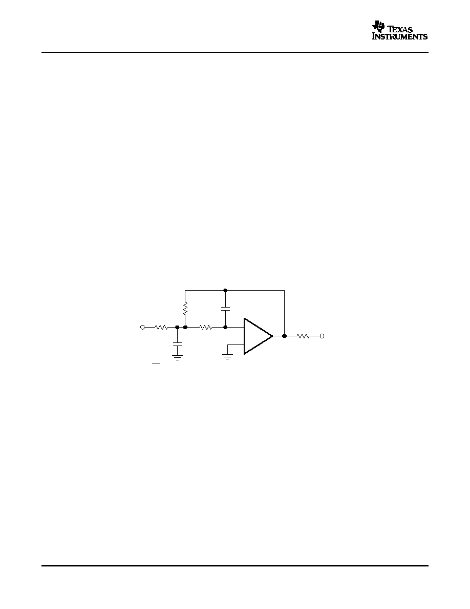
D/A OUTPUT FILTER CIRCUITS
ş
2
3
1
OPA2134
+
V
OUT
R
4
C
2
C
1
R
3
R
2
R
1
V
IN
A
V
+ *
R
2
R
1
S0053-01
PCB LAYOUT GUIDELINES
PCM1680
SLES133 ş MARCH 2005
APPLICATION INFORMATION (continued)
The PCM1680 requires 5 V for the analog supply and digital supply. The 5-V supply is used to power not only
the DAC analog and output filter circuitry, but also the digital filter and serial interface circuitry. For best
performance, a 5-V supply using a linear regulator is recommended.
Four capacitors are required for supply bypassing, as shown in Figure 32. These capacitors should be located as
close as possible to the PCM1680 package. The 10-
Á
F capacitor should be tantalum or aluminum electrolytic,
while the three 1-
Á
F capacitors are ceramic.
Delta-sigma D/A converters use noise shaping techniques to improve in-band signal-to-noise ratio (SNR)
performance at the expense of generating increased out-of-band noise above the Nyquist frequency, or f
S
/2. The
out-of-band noise must be low-pass filtered in order to provide optimal converter performance. This is
accomplished by a combination of on-chip and external low-pass filtering.
Figure 31 and Figure 33 show the recommended external low-pass active filter circuits for dual- and
single-supply applications. These circuits are second-order Butterworth filters using a multiple-feedback (MFB)
circuit arrangement, which reduces sensitivity to passive component variations over frequency and temperature.
For more information regarding MFB active filter design, see Dynamic Performance Testing of Digital Audio D/A
Converters (
SBAA055
).
Because the overall system performance is defined by the quality of the D/A converters and their associated
analog output circuitry, high-quality audio operational amplifiers are recommended for the active filters. Texas
Instruments' OPA2134 and OPA2353 dual operational amplifiers are shown in Figure 31 and Figure 33, and are
recommended for use with the PCM1680.
Figure 33. Dual-Supply Filter Circuit
A typical PCB floor plan for the PCM1680 is shown in Figure 34. A ground plane is recommended, with the
analog and digital sections being isolated from one another using a split or cut in the circuit board. The PCM1680
should be oriented with the digital I/O pins facing the ground plane split/cut to allow for short, direct connections
to the digital audio interface and control signals originating from the digital section of the board.
Separate power supplies are recommended for the digital and analog sections of the board. This prevents the
switching noise present on the digital supply from contaminating the analog power supply and degrading the
dynamic performance of the PCM1680. In cases where a common 5-V supply must be used for the analog and
digital sections, an inductance (RF choke, ferrite bead) should be placed between the analog and digital 5-V
supply connections to avoid coupling of the digital switching noise into the analog circuitry. Figure 35 shows the
recommended approach for single-supply applications.
30

www.ti.com
Digital Logic
and
Audio
Processor
Digital Power
+V
D
DGND
Digital Section
Analog Section
Return Path for Digital Signals
Analog Power
+V
S
AGND
şV
S
+5VA
Digital
Ground
Analog
Ground
Output
Circuits
PCM1680
AGND
V
DD
B0031-02
DGND
V
CC
V
DD
Digital Section
Analog Section
RF Choke or Ferrite Bead
Power Supplies
Common
Ground
Output
Circuits
AGND
V
DD
+V
S
+5V
şV
S
AGND
PCM1680
B0032-02
Digital Logic
and
Audio
Processor
V
CC
DGND
PCM1680
SLES133 ş MARCH 2005
APPLICATION INFORMATION (continued)
Figure 34. Recommended PCB Layout
Figure 35. Single-Supply PCB Layout
31
PACKAGING INFORMATION
Orderable Device
Status
(1)
Package
Type
Package
Drawing
Pins Package
Qty
Eco Plan
(2)
Lead/Ball Finish
MSL Peak Temp
(3)
PCM1680DBQ
ACTIVE
SSOP/
QSOP
DBQ
28
48
Green (RoHS &
no Sb/Br)
CU NIPDAU
Level-2-260C-1 YEAR
PCM1680DBQR
ACTIVE
SSOP/
QSOP
DBQ
28
2000 Green (RoHS &
no Sb/Br)
CU NIPDAU
Level-2-260C-1 YEAR
(1)
The marketing status values are defined as follows:
ACTIVE: Product device recommended for new designs.
LIFEBUY: TI has announced that the device will be discontinued, and a lifetime-buy period is in effect.
NRND: Not recommended for new designs. Device is in production to support existing customers, but TI does not recommend using this part in
a new design.
PREVIEW: Device has been announced but is not in production. Samples may or may not be available.
OBSOLETE: TI has discontinued the production of the device.
(2)
Eco
Plan
-
The
planned
eco-friendly
classification:
Pb-Free
(RoHS)
or
Green
(RoHS
&
no
Sb/Br)
-
please
check
http://www.ti.com/productcontent
for the latest availability information and additional product content details.
TBD: The Pb-Free/Green conversion plan has not been defined.
Pb-Free (RoHS): TI's terms "Lead-Free" or "Pb-Free" mean semiconductor products that are compatible with the current RoHS requirements
for all 6 substances, including the requirement that lead not exceed 0.1% by weight in homogeneous materials. Where designed to be soldered
at high temperatures, TI Pb-Free products are suitable for use in specified lead-free processes.
Green (RoHS & no Sb/Br): TI defines "Green" to mean Pb-Free (RoHS compatible), and free of Bromine (Br) and Antimony (Sb) based flame
retardants (Br or Sb do not exceed 0.1% by weight in homogeneous material)
(3)
MSL, Peak Temp. -- The Moisture Sensitivity Level rating according to the JEDEC industry standard classifications, and peak solder
temperature.
Important Information and Disclaimer:The information provided on this page represents TI's knowledge and belief as of the date that it is
provided. TI bases its knowledge and belief on information provided by third parties, and makes no representation or warranty as to the
accuracy of such information. Efforts are underway to better integrate information from third parties. TI has taken and continues to take
reasonable steps to provide representative and accurate information but may not have conducted destructive testing or chemical analysis on
incoming materials and chemicals. TI and TI suppliers consider certain information to be proprietary, and thus CAS numbers and other limited
information may not be available for release.
In no event shall TI's liability arising out of such information exceed the total purchase price of the TI part(s) at issue in this document sold by TI
to Customer on an annual basis.
PACKAGE OPTION ADDENDUM
www.ti.com
1-Aug-2005
Addendum-Page 1

IMPORTANT NOTICE
Texas Instruments Incorporated and its subsidiaries (TI) reserve the right to make corrections, modifications,
enhancements, improvements, and other changes to its products and services at any time and to discontinue
any product or service without notice. Customers should obtain the latest relevant information before placing
orders and should verify that such information is current and complete. All products are sold subject to TI's terms
and conditions of sale supplied at the time of order acknowledgment.
TI warrants performance of its hardware products to the specifications applicable at the time of sale in
accordance with TI's standard warranty. Testing and other quality control techniques are used to the extent TI
deems necessary to support this warranty. Except where mandated by government requirements, testing of all
parameters of each product is not necessarily performed.
TI assumes no liability for applications assistance or customer product design. Customers are responsible for
their products and applications using TI components. To minimize the risks associated with customer products
and applications, customers should provide adequate design and operating safeguards.
TI does not warrant or represent that any license, either express or implied, is granted under any TI patent right,
copyright, mask work right, or other TI intellectual property right relating to any combination, machine, or process
in which TI products or services are used. Information published by TI regarding third-party products or services
does not constitute a license from TI to use such products or services or a warranty or endorsement thereof.
Use of such information may require a license from a third party under the patents or other intellectual property
of the third party, or a license from TI under the patents or other intellectual property of TI.
Reproduction of information in TI data books or data sheets is permissible only if reproduction is without
alteration and is accompanied by all associated warranties, conditions, limitations, and notices. Reproduction
of this information with alteration is an unfair and deceptive business practice. TI is not responsible or liable for
such altered documentation.
Resale of TI products or services with statements different from or beyond the parameters stated by TI for that
product or service voids all express and any implied warranties for the associated TI product or service and
is an unfair and deceptive business practice. TI is not responsible or liable for any such statements.
Following are URLs where you can obtain information on other Texas Instruments products and application
solutions:
Products
Applications
Amplifiers
amplifier.ti.com
Audio
www.ti.com/audio
Data Converters
dataconverter.ti.com
Automotive
www.ti.com/automotive
DSP
dsp.ti.com
Broadband
www.ti.com/broadband
Interface
interface.ti.com
Digital Control
www.ti.com/digitalcontrol
Logic
logic.ti.com
Military
www.ti.com/military
Power Mgmt
power.ti.com
Optical Networking
www.ti.com/opticalnetwork
Microcontrollers
microcontroller.ti.com
Security
www.ti.com/security
Telephony
www.ti.com/telephony
Video & Imaging
www.ti.com/video
Wireless
www.ti.com/wireless
Mailing Address:
Texas Instruments
Post Office Box 655303 Dallas, Texas 75265
Copyright
2005, Texas Instruments Incorporated