PCI1225 GHK/PDV
PC CARD CONTROLLERS
SCPS035B MAY 1998 REVISED MAY 2000
1
POST OFFICE BOX 655303
·
DALLAS, TEXAS 75265
D
PCI Bus Power Management Interface
Specification 1.0 Compliant
D
ACPI 1.0 Compliant
D
Fully Compatible With the Intel
TM
430TX
(Mobile Triton II) Chipset
D
Packaged in a 208-Pin Low-Profile QFP
(PDV) or GHK High Density Ball Grid Array
(BGA)
D
PCI Local Bus Specification Revision 2.2
Compliant
D
1997 PC Card Standard Compliant
D
PC 99 Compliant
D
3.3-V Core Logic With Universal PCI
Interfaces Compatible With 3.3-V and 5-V
PCI Signaling Environments
D
Mix-and-Match 5-V/3.3-V 16-bit PC Cards
and 3.3-V CardBus Cards
D
Supports Two PC Card or CardBus Slots
With Hot Insertion and Removal
D
Uses Serial Interface to TI TPS2202/2206
Dual-Slot PC Card Power Switch
D
Supports Burst Transfers to Maximize Data
Throughput on the PCI Bus and CardBus
Bus
D
Supports Parallel PCI Interrupts, Parallel
ISA IRQ and Parallel PCI Interrupts, Serial
ISA IRQ With Parallel PCI Interrupts, and
Serial ISA IRQ and PCI Interrupts
D
Serial EEPROM Interface for Loading
Subsystem ID and Subsystem Vendor ID
D
Pipelined Architecture Allows Greater Than
130-MBps Throughput From
CardBus-to-PCI and From PCI-to-CardBus
D
Supports up to Five General-Purpose I/Os
D
Programmable Output Select for CLKRUN
D
Multifunction PCI Device With Separate
Configuration Space for Each Socket
D
Five PCI Memory Windows and Two I/O
Windows Available for Each R2 Socket
D
Two I/O Windows and Two Memory
Windows Available to Each CardBus
Socket
D
Exchangeable Card Architecture (ExCA)
Compatible Regesters Are Mapped in
Memory and I/O Space
D
Intel 82365SL-DF Register Compatible
D
Supports Distributed DMA (DDMA) and
PC/PCI DMA
D
Supports 16-Bit DMA on Both PC Card
Sockets
D
Supports Ring Indicate, SUSPEND, PCI
CLKRUN, and CardBus CCLKRUN
D
LED Activity Pins
D
Supports PCI Bus Lock (LOCK)
D
Advanced Submicron, Low-Power CMOS
Technology
Description
2
. . . . . . . . . . . . . . . . . . . . . . . . . . . . . . . . . . . . . . . . . . . . . . . . . . . . .
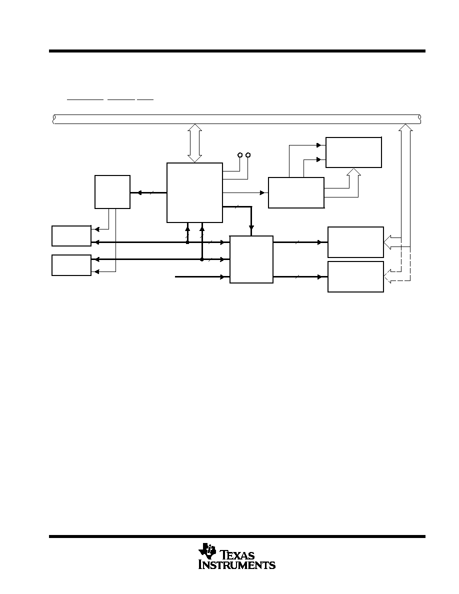
System Block Diagram
3
. . . . . . . . . . . . . . . . . . . . . . . . . . . . . . . . . . . . . . . . . . .
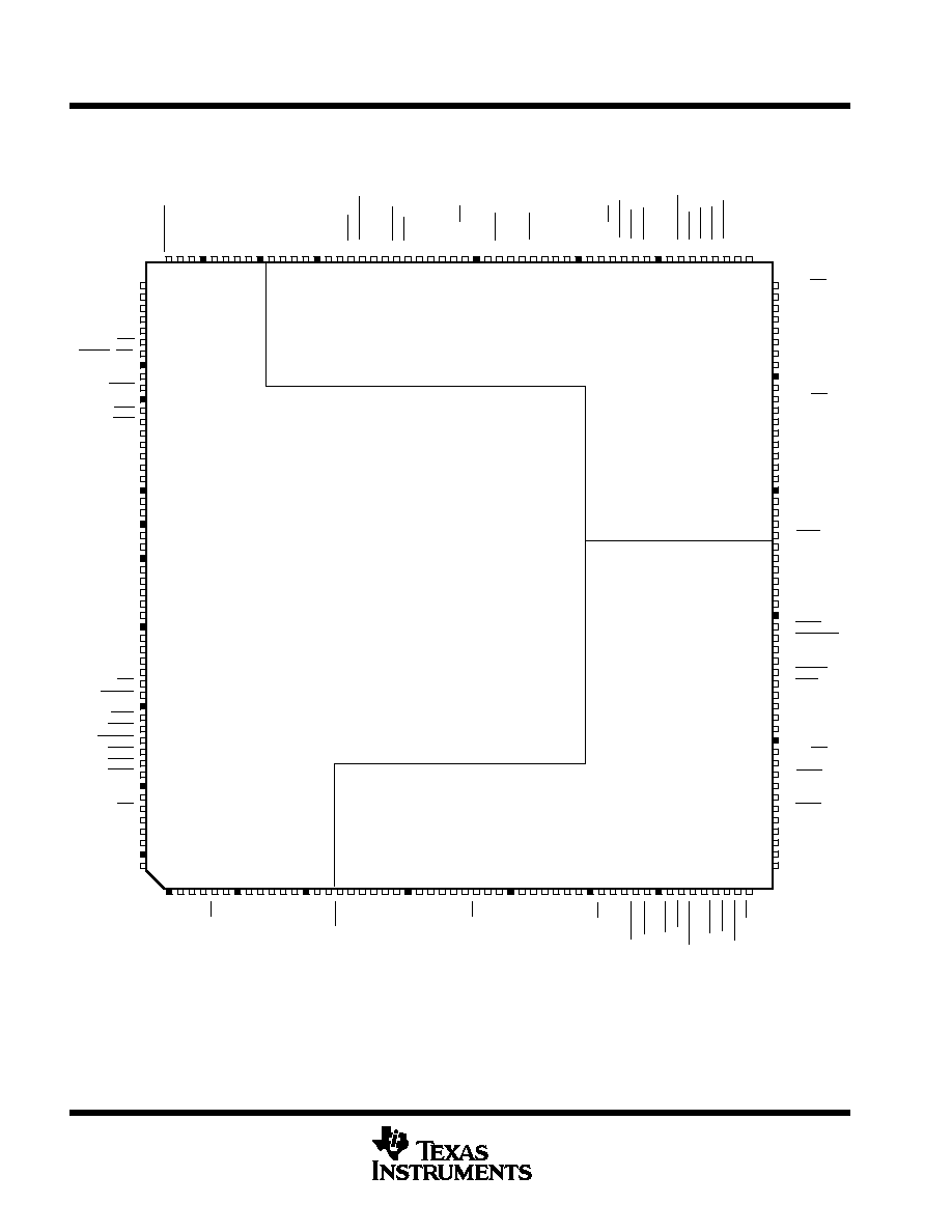
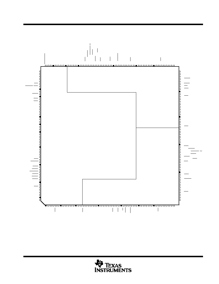
Terminal Assignments
4
. . . . . . . . . . . . . . . . . . . . . . . . . . . . . . . . . . . . . . . . . . . .
Signal Name/Terminal Number Sort Tables
6
. . . . . . . . . . . . . . . . . . . . . . . . . .
Terminal Functions
12
. . . . . . . . . . . . . . . . . . . . . . . . . . . . . . . . . . . . . . . . . . . .
Power Supply Sequencing
22
. . . . . . . . . . . . . . . . . . . . . . . . . . . . . . . . . . . . . .
I/O Characteristics
22
. . . . . . . . . . . . . . . . . . . . . . . . . . . . . . . . . . . . . . . . . . . . .
Clamping Rail Voltages
22
. . . . . . . . . . . . . . . . . . . . . . . . . . . . . . . . . . . . . . . . .
Peripheral Component Interconnect (PCI) Interface
23
. . . . . . . . . . . . . . . .
PC Card Applications
24
. . . . . . . . . . . . . . . . . . . . . . . . . . . . . . . . . . . . . . . . . .
Serial Bus Interface
30
. . . . . . . . . . . . . . . . . . . . . . . . . . . . . . . . . . . . . . . . . . . .
Programmable Interrupt Subsystem
36
. . . . . . . . . . . . . . . . . . . . . . . . . . . . . .
Power Management Overview
41
. . . . . . . . . . . . . . . . . . . . . . . . . . . . . . . . . .
PC Card Controller Programming Model
45
. . . . . . . . . . . . . . . . . . . . . . . . . .
PCI Configuration Registers (Functions 0 and 1)
46
. . . . . . . . . . . . . . . . . . .
ExCA Compatibility Registers (Functions 0 and 1)
83
. . . . . . . . . . . . . . . . . .
CardBus Socket Registers (Functions 0 and 1)
106
. . . . . . . . . . . . . . . . . . . . . .
Distributed DMA (DDMA) Registers
114
. . . . . . . . . . . . . . . . . . . . . . . . . . . . . . . .
Absolute Maximum Ratings
119
. . . . . . . . . . . . . . . . . . . . . . . . . . . . . . . . . . . . . . .
Recommended Operating Conditions
120
. . . . . . . . . . . . . . . . . . . . . . . . . . . . . .
Electrical Characteristics
121
. . . . . . . . . . . . . . . . . . . . . . . . . . . . . . . . . . . . . . . . .
PCI Clock/Reset Timing Requirements
122
. . . . . . . . . . . . . . . . . . . . . . . . . . . . .
PCI Timing Requirements
122
. . . . . . . . . . . . . . . . . . . . . . . . . . . . . . . . . . . . . . . .
Parameter Measurement Information
123
. . . . . . . . . . . . . . . . . . . . . . . . . . . . . . .
PCI Bus Parameter Measurement Information
124
. . . . . . . . . . . . . . . . . . . . . . .
PC Card Cycle Timing
125
. . . . . . . . . . . . . . . . . . . . . . . . . . . . . . . . . . . . . . . . . . .
Timing Requirements (Memory Cycles)
126
. . . . . . . . . . . . . . . . . . . . . . . . . . . . .
Timing Requirements (I/O Cycles)
126
. . . . . . . . . . . . . . . . . . . . . . . . . . . . . . . . .
Switching Characteristics (Miscellaneous
127
. . . . . . . . . . . . . . . . . . . . . . . . . . .
PC Card Parameter Measurement Information
128
. . . . . . . . . . . . . . . . . . . . . . .
Mechanical Data
129
. . . . . . . . . . . . . . . . . . . . . . . . . . . . . . . . . . . . . . . . . . . . . . . .
Table of Contents
Please be aware that an important notice concerning availability, standard warranty, and use in critical applications of
Texas Instruments semiconductor products and disclaimers thereto appears at the end of this data sheet.
Copyright
©
2000, Texas Instruments Incorporated
Intel is a trademark of Intel Corporation.
PRODUCTION DATA information is current as of publication date.
Products conform to specifications per the terms of Texas Instruments
standard warranty. Production processing does not necessarily include
testing of all parameters.

PCI1225 GHK/PDV
PC CARD CONTROLLERS
SCPS035B MAY 1998 REVISED MAY 2000
2
POST OFFICE BOX 655303
·
DALLAS, TEXAS 75265
description
The TI PCI1225 is a high-performance PCI-to-PC Card controller that supports two independent card sockets
compliant with the 1997 PC Card Standard. The PCI1225 provides a rich feature set that makes it the best
choice for bridging between PCI and PC Cards in both notebook and desktop computers. The 1997 PC Card
Standard retains the 16-bit PC Card specification defined in PCMCIA Release 2.2 and defines the new 32-bit
PC Card (CardBus), capable of full 32-bit data transfers at 33 MHz. The PCI1225 supports any combination
of 16-bit and CardBus PC Cards in the two sockets, powered at 5 V or 3.3 V, as required.
The PCI1225 is compliant with the PCI Local Bus Specification 2.2, and its PCI interface can act as either a PCI
master device or a PCI slave device. The PCI bus mastering is initiated during 16-bit PC Card DMA transfers
or CardBus PC Card bridging transactions. The PCI1225 is also compliant with the latest
PCI Bus Power
Management Interface Specification.
All card signals are internally buffered to allow hot insertion and removal without external buffering. The PCI1225
is register compatible with the Intel 82365SL-DF ExCA controller. The PCI1225 internal data path logic allows
the host to access 8-, 16-, and 32-bit cards using full 32-bit PCI cycles for maximum performance. Independent
buffering and a pipeline architacture provide an unsurpassed performance level with sustained bursting. The
PCI1225 can also be programmed to accept fast posted writes to improve system-bus utilization.
Multiple system-interrupt signaling options are provided, including: parallel PCI, parallel ISA, serialized ISA, and
serialized PCI. Furthermore, general-purpose inputs and outputs are provided for the board designer to
implement sideband functions. Many other features designed into the PCI1225, such as socket activity
light-emitting diode (LED) outputs, are discussed in detail throughout the design specification.
An advanced complementary metal-oxide semiconductor (CMOS) process is used to achieve low
system-power consumption while operating at PCI clock rates up to 33 MHz. Several low-power modes enable
the host power management system to further reduce power consumption.
Unused PCI1225 inputs must be pulled up using a 43-k
W
resistor.