PCF8574
REMOTE 8 BIT I/O EXPANDER FOR I
2
C BUS
SCPS068C - JULY 2001 - REVISED JANUARY 2004
1
POST OFFICE BOX 655303
À
DALLAS, TEXAS 75265
D
Low Standby-Current Consumption of
10
Á
A Maximum
D
I
2
C to Parallel-Port Expander
D
Open-Drain Interrupt Output
D
Compatible With Most Microcontrollers
D
Latched Outputs With High-Current Drive
Capability for Directly Driving LEDs
D
Latch-Up Performance Exceeds 100 mA Per
JESD 78, Class II
1
2
3
4
5
6
7
8
16
15
14
13
12
11
10
9
A0
A1
A2
P0
P1
P2
P3
GND
V
CC
SDA
SCL
INT
P7
P6
P5
P4
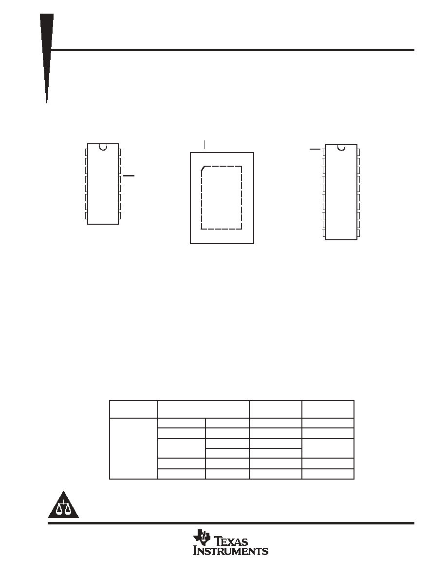
DW OR N PACKAGE
(TOP VIEW)
1
2
3
4
5
6
7
8
9
10
20
19
18
17
16
15
14
13
12
11
INT
SCL
NC
SDA
V
CC
A0
A1
NC
A2
P0
P7
P6
NC
P5
P4
GND
P3
NC
P2
P1
DGV OR PW PACKAGE
(TOP VIEW)
NC - No internal connection
RGY PACKAGE
(TOP VIEW)
1
20
10
11
2
3
4
5
6
7
8
9
19
18
17
16
15
14
13
12
P6
NC
P5
P4
GND
P3
NC
P2
SCL
NC
SDA
V
CC
A0
A1
NC
A2
INT
P1
P7
P0
NC - No internal connection
description/ordering information
This 8-bit input/output (I/O) expander for the two-line bidirectional bus (I
2
C) is designed for 2.5-V to 6-V V
CC
operation.
The PCF8574 provides general-purpose remote I/O expansion for most microcontroller families via the I
2
C
interface [serial clock (SCL), serial data (SDA)].
The device features an 8-bit quasi-bidirectional I/O port (P0-P7), including latched outputs with high-current
drive capability for directly driving LEDs. Each quasi-bidirectional I/O can be used as an input or output without
the use of a data-direction control signal. At power on, the I/Os are high. In this mode, only a current source to
V
CC
is active. An additional strong pullup to V
CC
allows fast rising edges into heavily loaded outputs. This device
turns on when an output is written high and is switched off by the negative edge of SCL. The I/Os should be
high before being used as inputs.
ORDERING INFORMATION
TA
PACKAGE
ORDERABLE
PART NUMBER
TOP-SIDE
MARKING
QFN - RGY
Tape and reel
PCF8574RGYR
PF574
PDIP - N
Tube
PCF8574N
PCF8574N
-40
░
C to 85
░
C
SOIC - DW
Tube
PCF8574DW
PCF8574
-40
░
C to 85
░
C
SOIC - DW
Tape and reel
PCF8574DWR
PCF8574
TSSOP - PW
Tape and reel
PCF8574PWR
PF574
TVSOP - DGV
Tape and reel
PCF8574DGVR
PF574
Package drawings, standard packing quantities, thermal data, symbolization, and PCB design
guidelines are available at www.ti.com/sc/package.
Copyright
2004, Texas Instruments Incorporated
Please be aware that an important notice concerning availability, standard warranty, and use in critical applications of
Texas Instruments semiconductor products and disclaimers thereto appears at the end of this data sheet.
PRODUCTION DATA information is current as of publication date.
Products conform to specifications per the terms of Texas Instruments
standard warranty. Production processing does not necessarily include
testing of all parameters.

PCF8574
REMOTE 8 BIT I/O EXPANDER FOR I
2
C BUS
SCPS068C - JULY 2001 - REVISED JANUARY 2004
2
POST OFFICE BOX 655303
À
DALLAS, TEXAS 75265
description/ordering information (continued)
The PCF8574 provides an open-drain output (INT) that can be connected to the interrupt input of a
microcontroller. An interrupt is generated by any rising or falling edge of the port inputs in the input mode. After
time t
iv
, INT is valid. Resetting and reactivating the interrupt circuit is achieved when data on the port is changed
to the original setting or data is read from, or written to, the port that generated the interrupt. Resetting occurs
in the read mode at the acknowledge bit after the rising edge of the SCL signal or in the write mode at the
acknowledge bit after the high-to-low transition of the SCL signal. Interrupts that occur during the acknowledge
clock pulse can be lost (or be very short) due to the resetting of the interrupt during this pulse. Each change of
the I/Os after resetting is detected and, after the next rising clock edge, is transmitted as INT. Reading from,
or writing to, another device does not affect the interrupt circuit.
By sending an interrupt signal on this line, the remote I/O can inform the microcontroller if there is incoming data
on its ports without having to communicate via the I
2
C bus. Therefore, the PCF8574 can remain a simple slave
device.
logic diagram (positive logic)
14
I/O
Port
4
5
6
7
9
10
11
12
P0
P1
P2
P3
P4
P5
P6
P7
Shift
Register
8 Bit
LP Filter
Interrupt
Logic
I2C Bus
Control
Input
Filter
15
Power-On
Reset
Read Pulse
Write Pulse
PCF8574
3
2
1
13
16
8
GND
VCC
SDA
SCL
A2
A1
A0
INT
Pin numbers shown are for the DW and N packages.
PCF8574
REMOTE 8 BIT I/O EXPANDER FOR I
2
C BUS
SCPS068C - JULY 2001 - REVISED JANUARY 2004
3
POST OFFICE BOX 655303
À
DALLAS, TEXAS 75265
simplified schematic diagram of each P-port input/output
To Interrupt
Logic
P0-P7
VCC
GND
CI
S
D
Q
FF
CI
S
D
Q
FF
Write Pulse
Data From
Shift Register
Power-On
Reset
Read Pulse
Data to
Shift Register
100
Á
A
I
2
C interface
I
2
C communication with this device is initiated by a master sending a start condition, a high-to-low transition on
the SDA I/O while the SCL input is high. After the start condition, the device address byte is sent, most-significant
bit (MSB) first, including the data direction bit (R/W). This device does not respond to the general call address.
After receiving the valid address byte, this device responds with an acknowledge, a low on the SDA I/O during
the high of the acknowledge-related clock pulse. The address inputs (A0-A2) of the slave device must not be
changed between the start and the stop conditions.
The data byte follows the address acknowledge. If the R/W bit is high, the data from this device are the values
read from the P port. If the R/W bit is low, the data are from the master, to be output to the P port. The data byte
is followed by an acknowledge sent from this device. If other data bytes are sent from the master, following the
acknowledge, they are ignored by this device. Data are output only if complete bytes are received and
acknowledged. The output data will be valid at time t
pv
after the low-to-high transition of SCL and during the clock
cycle for the acknowledge.
A stop condition, which is a low-to-high transition on the SDA I/O while the SCL input is high, is sent by the
master.
INTERFACE DEFINITION
BYTE
BIT
BYTE
7 (MSB)
6
5
4
3
2
1
0 (LSB)
I2C slave address
L
H
L
L
A2
A1
AO
R/W
I/O data bus
P7
P6
P5
P4
P3
P2
P1
P0

PCF8574
REMOTE 8 BIT I/O EXPANDER FOR I
2
C BUS
SCPS068C - JULY 2001 - REVISED JANUARY 2004
4
POST OFFICE BOX 655303
À
DALLAS, TEXAS 75265
ADDRESS REFERENCE
INPUTS
I2C-BUS SLAVE ADDRESS
A2
A1
A0
I2C-BUS SLAVE ADDRESS
L
L
L
32 (decimal), 20 (hexadecimal)
L
L
H
33 (decimal), 21 (hexadecimal)
L
H
L
34 (decimal), 22 (hexadecimal)
L
H
H
35 (decimal), 23 (hexadecimal)
H
L
L
36 (decimal), 24 (hexadecimal)
H
L
H
37 (decimal), 25 (hexadecimal)
H
H
L
38 (decimal), 26 (hexadecimal)
H
H
H
39 (decimal), 27 (hexadecimal)
absolute maximum ratings over operating free-air temperature range (unless otherwise noted)
Supply voltage range, V
CC
-0.5 V to 7 V
. . . . . . . . . . . . . . . . . . . . . . . . . . . . . . . . . . . . . . . . . . . . . . . . . . . . . . . . . .
Input voltage range, V
I
(see Note 1)
-0.5 V to V
CC
+ 0.5 V
. . . . . . . . . . . . . . . . . . . . . . . . . . . . . . . . . . . . . . . . . . .
Output voltage range, V
O
(see Note 1)
-0.5 V to V
CC
+ 0.5 V
. . . . . . . . . . . . . . . . . . . . . . . . . . . . . . . . . . . . . . . .
Input clamp current, I
IK
(V
I
< 0 )
-20 mA
. . . . . . . . . . . . . . . . . . . . . . . . . . . . . . . . . . . . . . . . . . . . . . . . . . . . . . . . . .
Output clamp current, I
OK
(V
O
< 0)
-20 mA
. . . . . . . . . . . . . . . . . . . . . . . . . . . . . . . . . . . . . . . . . . . . . . . . . . . . . . . .
Input/Output clamp current, I
OK
(V
O
< 0 or V
O
> V
CC
)
▒
400
Á
A
. . . . . . . . . . . . . . . . . . . . . . . . . . . . . . . . . . . . . .
Continuous output low current, I
OL
(V
O
= 0 to V
CC
) 50
mA
. . . . . . . . . . . . . . . . . . . . . . . . . . . . . . . . . . . . . . . . . .
Continuous output high current, I
OH
(V
O
= 0 to V
CC
) -4
mA
. . . . . . . . . . . . . . . . . . . . . . . . . . . . . . . . . . . . . . . . .
Continuous current through V
CC
or GND
▒
100 mA
. . . . . . . . . . . . . . . . . . . . . . . . . . . . . . . . . . . . . . . . . . . . . . . . . .
Package thermal impedance,
JA
(see Note 2): DGV package
92
░
C/W
. . . . . . . . . . . . . . . . . . . . . . . . . . . . . . . .
(see Note 2): DW package
57
░
C/W
. . . . . . . . . . . . . . . . . . . . . . . . . . . . . . . . .
(see Note 2): N package
67
░
C/W
. . . . . . . . . . . . . . . . . . . . . . . . . . . . . . . . . . .
(see Note 2): PW package
83
░
C/W
. . . . . . . . . . . . . . . . . . . . . . . . . . . . . . . . .
(see Note 3): RGY package
37
░
C/W
. . . . . . . . . . . . . . . . . . . . . . . . . . . . . . . .
Storage temperature range, T
stg
-65
░
C to 150
░
C
. . . . . . . . . . . . . . . . . . . . . . . . . . . . . . . . . . . . . . . . . . . . . . . . . . .
Stresses beyond those listed under "absolute maximum ratings" may cause permanent damage to the device. These are stress ratings only, and
functional operation of the device at these or any other conditions beyond those indicated under "recommended operating conditions" is not
implied. Exposure to absolute-maximum-rated conditions for extended periods may affect device reliability.
NOTES:
1. The input negative-voltage and output voltage ratings may be exceeded if the input and output current ratings are observed.
2. The package thermal impedance is calculated in accordance with JESD 51-7.
3. The package thermal impedance is calculated in accordance with JESD 51-5.
recommended operating conditions
MIN
MAX
UNIT
VCC
Supply voltage
2.5
6
V
VIH
High-level input voltage
0.7
Î
VCC
VCC + 0.5
V
VIL
Low-level input voltage
-0.5
0.3
Î
VCC
V
IOH
High-level output current
-1
mA
IOL
Low-level output current
25
mA
TA
Operating free-air temperature
-40
85
░
C
PCF8574
REMOTE 8 BIT I/O EXPANDER FOR I
2
C BUS
SCPS068C - JULY 2001 - REVISED JANUARY 2004
5
POST OFFICE BOX 655303
À
DALLAS, TEXAS 75265
electrical characteristics over recommended operating free-air temperature range (unless
otherwise noted)
PARAMETER
TEST CONDITIONS
VCC
MIN
TYP
MAX
UNIT
VIK
Input diode clamp voltage
II = -18 mA
2.5 V to 6 V
-1.2
V
VPOR
Power-on reset voltage
VI = VCC or GND, IO = 0
6 V
1.3
2.4
V
IOH
P port
VO = GND
2.5 V to 6 V
30
300
Á
A
IOHT
P-port transient pullup current
High during acknowledge VOH = GND
2.5 V
-1
mA
SDA
VO = 0.4 V
2.5 V to 6 V
3
IOL
P port
VO = 1 V
5 V
10
25
mA
IOL
INT
VO = 0.4 V
2.5 V to 6 V
1.6
mA
SCL, SDA
▒
5
II
INT
VI = VCC or GND
2.5 V to 6 V
▒
5
Á
A
II
A0, A1, A2
VI = VCC or GND
2.5 V to 6 V
▒
5
Á
A
IIHL
P port
VI
VCC or VI
GND
2.5 V to 6 V
▒
400
Á
A
ICC
Operating mode
VI = VCC or GND, IO = 0, fSCL = 100 kHz
6 V
40
100
A
ICC
Standby mode
VI = VCC or GND, IO = 0
6 V
2.5
10
Á
A
Ci
SCL
VI = VCC or GND
2.5 V to 6 V
1.5
7
pF
Cio
SDA
VIO = VCC or GND
2.5 V to 6 V
3
7
pF
Cio
P port
VIO = VCC or GND
2.5 V to 6 V
4
10
pF
All typical values are at VCC = 5 V, TA = 25
░
C.
The power-on reset circuit resets the I2C-bus logic with VCC < VPOR and sets all I/Os to logic high (with current source to VCC).
I
2
C interface timing requirements over recommended operating free-air temperature range (unless
otherwise noted) (see Figure 1)
MIN
MAX
UNIT
fscl
I2C clock frequency
100
kHz
tsch
I2C clock high time
4
Á
s
tscl
I2C clock low time
4.7
Á
s
tsp
I2C spike time
100
ns
tsds
I2C serial data setup time
250
ns
tsdh
I2C serial data hold time
0
900
ns
ticr
I2C input rise time
1
Á
s
ticf
I2C input fall time
0.3
Á
s
tocf
I2C output fall time (10-pF to 400-pF bus)
300
ns
tbuf
I2C-bus free time between stop and start
4.7
Á
s
tsts
I2C start or repeated start condition setup
4.7
Á
s
tsth
I2C start or repeated start condition hold
4
Á
s
tsps
I2C stop-condition setup
4
Á
s
tvd
Valid data time
SCL low to SDA output valid
3.4
Á
s
Cb
I2C-bus capacitive load
400
pF