
FEATURES
D
UNITY-GAIN BANDWIDTH: 250MHz
D
WIDE BANDWIDTH: 100MHz GBW
D
HIGH SLEW RATE: 150V/
µ
s
D
LOW NOISE: 6.5nV/
Hz
D
RAIL-TO-RAIL I/O
D
HIGH OUTPUT CURRENT: > 100mA
D
EXCELLENT VIDEO PERFORMANCE:
Diff Gain: 0.02%, Diff Phase: 0.09
5
0.1dB Gain Flatness: 40MHz
D
LOW INPUT BIAS CURRENT: 3pA
D
QUIESCENT CURRENT: 4.9mA
D
THERMAL SHUTDOWN
D
SUPPLY RANGE: 2.5V to 5.5V
D
MicroSIZE AND PowerPAD
PACKAGES
APPLICATIONS
D
VIDEO PROCESSING
D
ULTRASOUND
D
OPTICAL NETWORKING, TUNABLE LASERS
D
PHOTODIODE TRANSIMPEDANCE AMPS
D
ACTIVE FILTERS
D
HIGH-SPEED INTEGRATORS
D
ANALOG-TO-DIGITAL (A/D) CONVERTER
INPUT BUFFERS
D
DIGITAL-TO-ANALOG (D/A) CONVERTER
OUTPUT AMPLIFIERS
D
BARCODE SCANNERS
D
COMMUNICATIONS
DESCRIPTION
The OPA354 series of high-speed, voltage-feedback
CMOS operational amplifiers are designed for video and
other applications requiring wide bandwidth. They are
unity-gain stable and can drive large output currents.
Differential gain is 0.02% and differential phase is 0.09
°
.
Quiescent current is only 4.9mA per channel.
The OPA354 series op amps are optimized for operation
on single or dual supplies as low as 2.5V (
±
1.25V) and up
to 5.5V (
±
2.75V). Common-mode input range extends
beyond the supplies. The output swing is within 100mV of
the rails, supporting wide dynamic range.
For applications requiring the full 100mA continuous
output current, single and dual SO-8 PowerPAD versions
are available.
The single version (OPA354), is available in the tiny
SOT23-5 and SO-8 PowerPAD packages. The dual
version (OPA2354) comes in the miniature MSOP-8 and
SO-8 PowerPAD packages. The quad version (OPA4354)
is offered in TSSOP-14 and SO-14 packages.
Multichannel versions feature completely independent
circuitry for lowest crosstalk and freedom from interaction.
All are specified over the extended -40
°
C to +125
°
C
temperature range.
OPAx357 RELATED PRODUCTS
FEATURES
PRODUCT
Shutdown Version of OPA354 Family
OPAx357
200MHz GBW, Rail-to-Rail Output, CMOS, Shutdown
OPAx355
200MHz GBW, Rail-to-Rail Output, CMOS
OPAx356
38MHz GBW, Rail-to-Rail Input/Output, CMOS
OPAx350/3
75MHz BW G = 2, Rail-to-Rail Output
OPAx631
150MHz BW G = 2, Rail-to-Rail Output
OPAx634
100MHz BW, Differential Input/Output, 3.3V Supply
THS412x
OPA354
V
OUT
V+
V
-
-
In
+In
OPA354
OPA2354
OPA4354
SBOS233C - MARCH 2002- REVISED APRIL 2004
250MHz, Rail-to-Rail I/O, CMOS
OPERATIONAL AMPLIFIERS
PRODUCTION DATA information is current as of publication date. Products
conform to specifications per the terms of Texas Instruments standard warranty.
Production processing does not necessarily include testing of all parameters.
www.ti.com
Copyright
2002-2004, Texas Instruments Incorporated
Please be aware that an important notice concerning availability, standard warranty, and use in critical applications of Texas Instruments
semiconductor products and disclaimers thereto appears at the end of this data sheet.
All trademarks are the property of their respective owners.
OPA354
OPA2354
OPA4354
SBOS233C - MARCH 2002- REVISED APRIL 2004
www.ti.com
2
ABSOLUTE MAXIMUM RATINGS
(1)
Supply Voltage, V+ to V-
7.5V
. . . . . . . . . . . . . . . . . . . . . . . . . . . . . .
Signal Input Terminals Voltage(2)
(V-) - (0.5V) to (V+) + (0.5V)
. . .
Current(2)
10mA
. . . . . . . . . . . . . . . . . . . . .
Output Short-Circuit(3)
Continuous
. . . . . . . . . . . . . . . . . . . . . . . . . .
Operating Temperature
-55
°
C to +150
°
C
. . . . . . . . . . . . . . . . . . . . . .
Storage Temperature
-65
°
C to +150
°
C
. . . . . . . . . . . . . . . . . . . . . . . .
Junction Temperature
+150
°
C
. . . . . . . . . . . . . . . . . . . . . . . . . . . . . . .
Lead Temperature (soldering, 10s)
+300
°
C
. . . . . . . . . . . . . . . . . . . . .
(1) Stresses above these ratings may cause permanent damage.
Exposure to absolute maximum conditions for extended periods
may degrade device reliability. These are stress ratings only, and
functional operation of the device at these or any other conditions
beyond those specified is not supported.
(2) Input terminals are diode-clamped to the power-supply rails.
Input signals that can swing more than 0.5V beyond the supply
rails should be current limited to 10mA or less.
(3) Short-circuit to ground, one amplifier per package.
ELECTROSTATIC
DISCHARGE SENSITIVITY
This integrated circuit can be damaged by ESD. Texas Instruments
recommends that all integrated circuits be handled with appropriate
precautions. Failure to observe proper handling and installation
procedures can cause damage.
ESD damage can range from subtle performance degradation to
complete device failure. Precision integrated circuits may be more
susceptible to damage because very small parametric changes could
cause the device not to meet its published specifications.
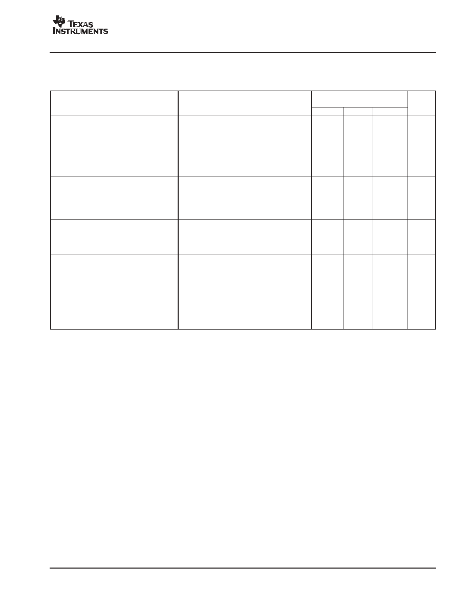
PACKAGE/ORDERING INFORMATION
(1)
PRODUCT
PACKAGE-LEAD
PACKAGE
DESIGNATOR(1)
SPECIFIED
TEMPERATURE
RANGE
PACKAGE
MARKING
ORDERING
NUMBER
TRANSPORT
MEDIA, QUANTITY
OPA354
SO-8 PowerPAD
DDA
-40
°
C to +125
°
C
OPA354A
OPA354AIDDA
Rails, 97
OPA354AIDDAR
Tape and Reel, 2500
OPA354
SOT23-5
DBV
-40
°
C to +125
°
C
OABI
OPA354AIDBVT
Tape and Reel, 250
OPA354AIDBVR
Tape and Reel, 3000
OPA2354
SO-8 PowerPAD
DDA
-40
°
C to +125
°
C
OPA2354A
OPA2354AIDDA
Rails, 97
OPA2354AIDDAR
Tape and Reel, 2500
OPA2354
MSOP-8
DGK
-40
°
C to +125
°
C
OACI
OPA2354AIDGKT
Tape and Reel, 250
OPA2354AIDGKR
Tape and Reel, 2500
OPA4354
SO-14
D
-40
°
C to +125
°
C
OPA4354A
OPA4354AID
Rails, 58
OPA4354AIDR
Tape and Reel, 2500
OPA4354
TSSOP-14
PW
-40
°
C to +125
°
C
OPA4354A
OPA4354AIPWT
Tape and Reel, 250
OPA4354AIPWR
Tape and Reel, 2500
(1) For the most current package and ordering information, see the Package Option Addendum located at the end of this data sheet.

OPA354
OPA2354
OPA4354
SBOS233C - MARCH 2002- REVISED APRIL 2004
www.ti.com
3
PIN CONFIGURATIONS
Top View
NOTES: (1) NC means no internal connection. (2) PowerPAD should be connected to V- or left floating.
1
2
3
4
8
7
6
5
NC
(1 )
V+
Out
NC
(1 )
NC
(1)
-
In
+In
V
-
OPA354
SO PowerPAD
(2)
1
2
3
5
4
V+
-
In
Out
V
-
+In
OPA354
SOT23
1
2
3
4
8
7
6
5
V+
Out B
-
In B
+In B
Out A
-
In A
+In A
V
-
OPA2354
SO PowerPAD
(2)
MSOP
A
B
1
2
3
4
5
6
7
14
13
12
11
10
9
8
Out D
-
In D
+In D
V
-
+In C
-
In C
Out C
Out A
-
In A
+In A
V+
+In B
-
In B
Out B
OPA4354
SO
TSSOP
B
C
D
A

OPA354
OPA2354
OPA4354
SBOS233C - MARCH 2002- REVISED APRIL 2004
www.ti.com
4
ELECTRICAL CHARACTERISTICS: V
S
= +2.7V to +5.5V Single-Supply
Boldface limits apply over the temperature range, T
A
= -40
°
C to +125
°
C.
All specifications at TA = +25
°
C, RF = 0
, RL = 1k
connected to VS/2, unless otherwise noted.
OPA354AI
OPA2354AI, OPA4354AI
PARAMETER
CONDITIONS
MIN
TYP
MAX
UNITS
OFFSET VOLTAGE
Input Offset Voltage
VOS
VS = +5V
±
2
±
8
mV
Specified Temperature Range
+
10
mV
vs Temperature
dV
OS
/dT
Specified Temperature Range
+
4
µ
V/
°
C
vs Power Supply
PSRR
VS = +2.7V to +5.5V, VCM = (VS/2) - 0.15V
±
200
±
800
µ
V/V
Specified Temperature Range
±
900
µ
V/V
INPUT BIAS CURRENT
Input Bias Current
IB
3
±
50
pA
Input Offset Current
IOS
±
1
±
50
pA
NOISE
Input Voltage Noise Density
en
f = 1MHz
6.5
nV/
Hz
Current Noise Density
in
f = 1MHz
50
fA/
Hz
INPUT VOLTAGE RANGE
Common-Mode Voltage Range
VCM
(V-) - 0.1
(V+) + 0.1
V
Common-Mode Rejection Ratio
CMRR
VS = +5.5V, -0.1V < VCM < +3.5V
66
80
dB
Specified Temperature Range
64
dB
VS = +5.5V, -0.1V < VCM < +5.6V
56
68
dB
Specified Temperature Range
55
dB
INPUT IMPEDANCE
Differential
1013 || 2
|| pF
Common-Mode
1013 || 2
|| pF
OPEN-LOOP GAIN
AOL
VS = +5V, +0.3V < VO < +4.7V
94
110
dB
Specified Temperature Range
VS = +5V, +0.4V < VO < +4.6V
90
dB
FREQUENCY RESPONSE
Small-Signal Bandwidth
f-3dB
G = +1, VO = 100mVPP, RF = 25
250
MHz
f-3dB
G = +2, VO = 100mVPP
90
MHz
Gain-Bandwidth Product
GBW
G = +10
100
MHz
Bandwidth for 0.1dB Gain Flatness
f0.1dB
G = +2, VO = 100mVPP
40
MHz
Slew Rate
SR
VS = +5V, G = +1, 4V Step
150
V/
µ
s
VS = +5V, G = +1, 2V Step
130
V/
µ
s
VS = +3V, G = +1, 2V Step
110
V/
µ
s
Rise-and-Fall Time
G = +1, VO = 200mVPP, 10% to 90%
2
ns
G = +1, VO = 2VPP, 10% to 90%
11
ns
Settling Time, 0.1%
VS = +5V, G = +1, 2V Output Step
30
ns
0.01%
60
ns
Overload Recovery Time
VIN
S
Gain = VS
5
ns
Harmonic Distortion
2nd-Harmonic
G = +1, f = 1MHz, VO = 2VPP, RL = 200
, VCM = 1.5V
-75
dBc
3rd-Harmonic
G = +1, f = 1MHz, VO = 2VPP, RL = 200
, VCM = 1.5V
-83
dBc
Differential Gain Error
NTSC, RL = 150
0.02
%
Differential Phase Error
NTSC, RL = 150
0.09
degrees
Channel-to-Channel Crosstalk
OPA2354
f = 5MHz
-100
dB
OPA4354
-84
dB
(1) See typical characteristics Output Voltage Swing vs Output Current.
(2) Specified by design.
OPA354
OPA2354
OPA4354
SBOS233C - MARCH 2002- REVISED APRIL 2004
www.ti.com
5
ELECTRICAL CHARACTERISTICS: V
S
= +2.7V to +5.5V Single-Supply (continued)
Boldface limits apply over the temperature range, T
A
= -40
°
C to +125
°
C.
All specifications at TA = +25
°
C, RF = 0
, RL = 1k
connected to VS/2, unless otherwise noted.
OPA354AI
OPA2354AI, OPA4354AI
PARAMETER
UNITS
MAX
TYP
MIN
CONDITIONS
OUTPUT
Voltage Output Swing from Rail
VS = +5V, RL = 1k
, AOL > 94dB
0.1
0.3
V
Specified Temperature Range
VS = +5V, RL = 1k
, AOL > 90dB
0.4
V
Output Current(1)(2), Single, Dual, Quad
IO
VS = +5V
100
mA
VS = +3V
50
mA
Closed-Loop Output Impedance
f < 100kHz
0.05
Open-Loop Output Resistance
RO
35
POWER SUPPLY
Specified Voltage Range
VS
2.7
5.5
V
Operating Voltage Range
2.5 to 5.5
V
Quiescent Current (per amplifier)
IQ
VS = +5V, Enabled, IO = 0
4.9
6
mA
Specified Temperature Range
7.5
mA
THERMAL SHUTDOWN
Junction Temperature
Shutdown
+160
°
C
Reset from Shutdown
+140
°
C
TEMPERATURE RANGE
Specified Range
-40
+125
°
C
Operating Range
-55
+150
°
C
Storage Range
-65
+150
°
C
Thermal Resistance
q
JA
°
C/W
SOT23-5, MSOP-8
150
°
C/W
TSSOP-14
100
°
C/W
SO-14
100
°
C/W
SO-8 PowerPAD
65
°
C/W
(1) See typical characteristics Output Voltage Swing vs Output Current.
(2) Specified by design.

OPA354
OPA2354
OPA4354
SBOS233C - MARCH 2002- REVISED APRIL 2004
www.ti.com
6
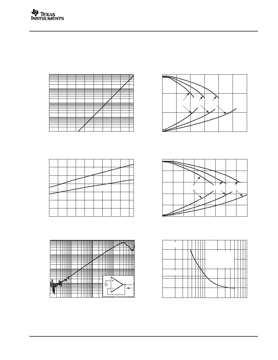
TYPICAL CHARACTERISTICS
At TA = +25
°
C, VS = 5V, G = +1, RF = 0
, RL = 1k
, and connected to VS/2, unless otherwise noted.
NONINVERTING SMALL-SIGNAL
FREQUENCY RESPONSE
Frequency (Hz)
N
o
r
m
a
l
iz
e
d
G
a
in
(
d
B)
10M
1M
100M
1G
100k
3
0
-
3
-
6
-
9
-
12
-
15
V
O
= 0.1V
PP
G = +2, R
F
= 604
G = +1
R
F
= 25
G = +5, R
F
= 604
G = +10, R
F
= 604
INVERTING SMALL-SIGNAL
FREQUENCY RESPONSE
Frequency (Hz)
N
o
r
m
a
l
iz
e
d
G
a
in
(
d
B)
10M
1M
100M
1G
100k
3
0
-
3
-
6
-
9
-
12
-
15
V
O
= 0.1V
PP
, R
F
= 604
G =
-
1
G =
-
5
G =
-
10
G =
-
2
NONINVERTING SMALL-SIGNAL STEP RESPONSE
Time (20ns/div)
O
u
tpu
t
V
o
l
t
a
g
e
(
40mV
/
di
v
)
NONINVERTING LARGE-SIGNAL STEP RESPONSE
Time (20ns/div)
O
u
tput
V
o
l
t
ag
e
(
500mV
/
d
i
v
)
0.1dB GAIN FLATNESS
Frequency (Hz)
N
o
rm
a
l
i
z
e
d
Ga
i
n
(d
B
)
10M
1M
100M
1G
100k
0.5
0.4
0.3
0.2
0.1
0
-
0.1
-
0.2
-
0.3
-
0.4
-
0.5
V
O
= 0.1V
PP
G = +1
R
F
= 25
G = +2
R
F
= 604
HARMONIC DISTORTION vs OUTPUT VOLTAGE
Output Voltage (V
PP
)
Ha
r
m
o
n
i
c
Di
s
t
o
r
ti
o
n
(
d
B
c
)
2
1
3
4
0
-
50
-
60
-
70
-
80
-
90
-
100
G =
-
1
f = 1MHz
R
L
= 200
2nd-Harmonic
3rd-Harmonic

OPA354
OPA2354
OPA4354
SBOS233C - MARCH 2002- REVISED APRIL 2004
www.ti.com
7
TYPICAL CHARACTERISTICS (continued)
At TA = +25
°
C, VS = 5V, G = +1, RF = 0
, RL = 1k
, and connected to VS/2, unless otherwise noted.
HARMONIC DISTORTION vs NONINVERTING GAIN
Gain (V/V)
Ha
r
m
o
n
i
c
Di
s
t
o
r
ti
o
n
(
d
B
c
)
10
1
-
50
-
60
-
70
-
80
-
90
-
100
V
O
= 2V
PP
f = 1MHz
R
L
= 200
3rd-Harmonic
2nd-Harmonic
HARMONIC DISTORTION vs INVERTING GAIN
Gain (V/V)
Ha
r
m
o
n
i
c
Di
s
t
o
r
ti
o
n
(
d
B
c
)
10
1
-
50
-
60
-
70
-
80
-
90
-
100
V
O
= 2V
PP
f = 1MHz
R
L
= 200
3rd-Harmonic
2nd-Harmonic
HARMONIC DISTORTION vs FREQUENCY
Frequency (Hz)
Ha
r
m
o
n
i
c
Di
s
t
o
r
ti
o
n
(
d
B
c
)
10M
1M
100k
-
50
-
60
-
70
-
80
-
90
-
100
G = +1
V
O
= 2V
PP
R
L
= 200
V
CM
= 1.5V
3rd-Harmonic
2nd-Harmonic
HARMONIC DISTORTION vs LOAD RESISTANCE
R
L
(
)
Ha
r
m
o
n
i
c
Di
s
t
o
r
ti
o
n
(
d
B
c
)
1k
100
-
50
-
60
-
70
-
80
-
90
-
100
G = +1
V
O
= 2V
PP
f = 1MHz
V
CM
= 1.5V
3rd-Harmonic
2nd-Harmonic
INPUT VOLTAGE AND CURRENT NOISE
SPECTRAL DENSITY vs FREQUENCY
Frequency (Hz)
Vo
l
t
a
g
e
N
o
i
s
e
(
n
V
/
Hz
)
,
C
u
r
r
en
t
N
oi
s
e
(
f
A
/
Hz
)
100M
10
100
1k
10k
100k
1M
10M
10k
1k
100
10
1
Current Noise
Voltage Noise
FREQUENCY RESPONSE FOR VARIOUS R
L
Frequency (Hz)
N
o
rm
a
l
i
z
e
d
Ga
i
n
(d
B
)
10M
1M
100M
1G
100k
3
0
-
3
-
6
-
9
-
12
-
15
R
L
= 10k
R
L
= 100
R
L
= 1k
R
L
= 50
G = +1
R
F
= 0
V
O
= 0.1V
PP
C
L
= 0pF

OPA354
OPA2354
OPA4354
SBOS233C - MARCH 2002- REVISED APRIL 2004
www.ti.com
8
TYPICAL CHARACTERISTICS (continued)
At TA = +25
°
C, VS = 5V, G = +1, RF = 0
, RL = 1k
, and connected to VS/2, unless otherwise noted.
FREQUENCY RESPONSE FOR VARIOUS C
L
Frequency (Hz)
N
o
rm
a
l
i
z
e
d
Ga
i
n
(d
B
)
10M
1M
100M
1G
100k
9
6
3
0
-
3
-
6
-
9
-
12
-
15
C
L
= 100pF
C
L
= 47pF
C
L
= 5.6pF
G = +1
V
O
= 0.1V
PP
R
S
= 0
RECOMMENDED R
S
vs CAPACITIVE LOAD
Capacitive Load (pF)
R
S
(
)
100
10
1k
1
160
140
120
100
80
60
40
20
0
OPA354
C
L
R
S
V
IN
V
O
1k
For 0.1dB
Flatness
FREQUENCY RESPONSE vs CAPACITIVE LOAD
Frequency (Hz)
N
o
r
m
a
l
iz
e
d
G
a
in
(
d
B)
100M
10M
1M
1G
100k
3
0
-
3
-
6
-
9
-
12
-
15
OPA354
C
L
R
S
V
IN
V
O
1k
C
L
= 47pF, R
S
= 140
C
L
= 100pF, R
S
= 120
C
L
= 5.6pF, R
S
= 0
G = +1
V
O
= 0.1V
PP
COMMON-MODE REJECTION RATIO AND
POWER-SUPPLY REJECTION RATIO vs FREQUENCY
Frequency (Hz)
CM
RR,
P
S
RR
(
d
B
)
10k
100k
1M
10M
100M
1G
100
80
60
40
20
0
PSRR
-
PSRR+
CMRR
OPEN-LOOP GAIN AND PHASE
Frequency (Hz)
O
pen-
Lo
op
P
has
e
(
degr
e
e
s
)
O
p
e
n
-
L
oop
G
a
i
n
(
d
B
)
10
100
1k
100k
10k
1M
10M
1G
100M
180
160
140
120
100
80
60
40
20
0
-
20
-
40
Phase
Gain
COMPOSITE VIDEO
DIFFERENTIAL GAIN AND PHASE
Number of 150
Loads
dG
/dP
(
%
/
degr
ee
s
)
3
2
4
1
0.8
0.7
0.6
0.5
0.4
0.3
0.2
0.1
0
dP
dG
OPA354
OPA2354
OPA4354
SBOS233C - MARCH 2002- REVISED APRIL 2004
www.ti.com
9
TYPICAL CHARACTERISTICS (continued)
At TA = +25
°
C, VS = 5V, G = +1, RF = 0
, RL = 1k
, and connected to VS/2, unless otherwise noted.
INPUT BIAS CURRENT vs TEMPERATURE
Temperature (
_
C)
Inp
u
t
B
i
a
s
C
ur
r
e
nt
(
p
A
)
65
85
105
5
25
45
135
125
-
55
-
35
-
15
10k
1k
100
10
1
OUTPUT VOLTAGE SWING vs OUTPUT CURRENT
FOR V
S
= 3V
Output Current (mA)
O
u
tput
V
o
l
t
ag
e
(
V
)
60
40
20
80
100
120
0
3
2
1
0
+125
_
C
+25
_
C
-
55
_
C
SUPPLY CURRENT vs TEMPERATURE
Temperature (
_
C)
S
u
p
p
l
y
C
ur
r
e
nt
(
m
A
)
65
85
105
5
25
45
135
125
-
55
-
35
-
15
7
6
5
4
3
2
1
0
V
S
= 5V
V
S
= 2.5V
OUTPUT VOLTAGE SWING vs OUTPUT CURRENT
FOR V
S
= 5V
Output Current (mA)
O
u
tput
V
o
l
t
ag
e
(
V
)
75
50
25
125
100
150
175
200
0
5
4
3
2
1
0
+25
_
C
-
55
_
C
+125
_
C
CLOSED-LOOP OUTPUT IMPEDANCE vs FREQUENCY
Frequency (Hz)
O
u
tp
u
t
Im
p
e
d
anc
e
(
)
10M
100M
1M
1G
100k
100
10
1
0.1
0.01
OPA354
Z
O
MAXIMUM OUTPUT VOLTAGE vs FREQUENCY
Frequency (MHz)
O
u
tp
ut
V
o
l
t
age
(
V
PP
)
10
100
1
6
5
4
3
2
1
0
V
S
= 5.5V
V
S
= 2.7V
Maximum Output
Voltage without
Slew-Rate
Induced Distortion

OPA354
OPA2354
OPA4354
SBOS233C - MARCH 2002- REVISED APRIL 2004
www.ti.com
10
TYPICAL CHARACTERISTICS (continued)
At TA = +25
°
C, VS = 5V, G = +1, RF = 0
, RL = 1k
, and connected to VS/2, unless otherwise noted.
OUTPUT SETTLING TIME TO 0.1%
Time (ns)
Ou
t
p
u
t
E
r
ro
r
(
%
)
30
40
10
20
100
50
60
70
80
90
0
0.5
0.4
0.3
0.2
0.1
0
-
0.1
-
0.2
-
0.3
-
0.4
-
0.5
V
O
= 2V
PP
OPEN-LOOP GAIN vs TEMPERATURE
Temperature (
_
C)
O
p
e
n
-
Loop
G
a
i
n
(
d
B
)
65
85
105
5
25
45
135
125
-
55
-
35
-
15
120
110
100
90
80
70
R
L
= 1k
OFFSET VOLTAGE PRODUCTION DISTRIBUTION
Offset Voltage (mV)
P
o
pul
ati
o
n
-
6
-
7
-
8
-
5
-
4
-
3
-
2
-
1
0 1
2 3
4
5 6
7 8
COMMON-MODE REJECTION RATIO AND
POWER-SUPPLY REJECTION RATIO vs TEMPERATURE
Temperature (
_
C)
CM
RR,
P
S
RR
(
d
B
)
65
85
105
5
25
45
135
125
-
55
-
35
-
15
100
90
80
70
60
50
Power-Supply Rejection Ratio
Common-Mode Rejection Ratio
CHANNEL-TO-CHANNEL CROSSTALK
Frequency (Hz)
C
r
os
s
t
a
l
k
,
In
pu
t
-
R
e
fe
r
r
e
d
(
dB
)
10M
1M
1G
100M
100k
0
-
20
-
40
-
60
-
80
-
100
-
120
OPA4354
OPA2354
OPA354
OPA2354
OPA4354
SBOS233C - MARCH 2002- REVISED APRIL 2004
www.ti.com
11
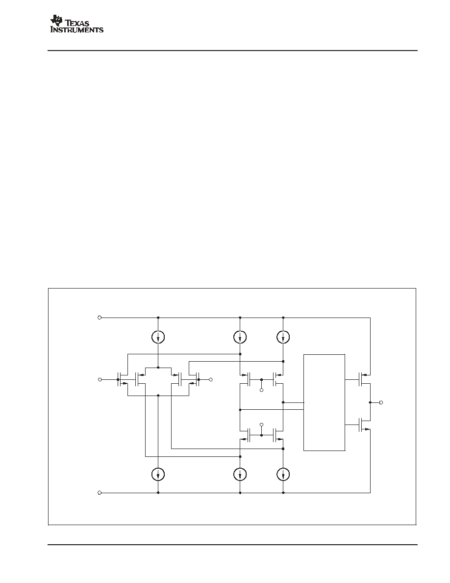
APPLICATIONS INFORMATION
The OPA354 is a CMOS, rail-to-rail I/O, high-speed,
voltage-feedback operational amplifier designed for video,
high-speed, and other applications. It is available as a
single, dual, or quad op amp.
The amplifier features a 100MHz gain bandwidth, and
150V/
µ
s slew rate, but it is unity-gain stable and can be
operated as a +1V/V voltage follower.
OPERATING VOLTAGE
The OPA354 is specified over a power-supply range of
+2.7V to +5.5V (
±
1.35V to
±
2.75V). However, the supply
voltage may range from +2.5V to +5.5V (
±
1.25V to
±
2.75V). Supply voltages higher than 7.5V (absolute
maximum) can permanently damage the amplifier.
Parameters that vary over supply voltage or temperature
are shown in the typical characteristics section of this data
sheet.
RAIL-TO-RAIL INPUT
The specified input common-mode voltage range of the
OPA354 extends 100mV beyond the supply rails. This is
achieved with a complementary input stage
an
N-channel input differential pair in parallel with a
P-channel differential pair, as shown in Figure 1. The
N-channel pair is active for input voltages close to the
positive rail, typically (V+) - 1.2V to 100mV above the
positive supply, while the P-channel pair is on for inputs
from 100mV below the negative supply to approximately
(V+) - 1.2V. There is a small transition region, typically
(V+) - 1.5V to (V+) - 0.9V, in which both pairs are on. This
600mV transition region can vary
±
500mV with process
variation. Thus, the transition region (both input stages on)
can range from (V+) - 2.0V to (V+) - 1.5V on the low end,
up to (V+) - 0.9V to (V+) - 0.4V on the high end.
A double-folded cascode adds the signal from the two
input pairs and presents a differential signal to the class AB
output stage.
RAIL-TO-RAIL OUTPUT
A class AB output stage with common-source transistors
is used to achieve rail-to-rail output. For high-impedance
loads (> 200
), the output voltage swing is typically
100mV from the supply rails. With 10
loads, a useful
output swing can be achieved while maintaining high
open-loop gain. See the typical characteristic curve Output
Voltage Swing vs Output Current.
V
BIAS1
V
BIAS2
V
IN
+
V
IN
-
Class AB
Control
Circuitry
V
O
V
-
(Ground)
V+
Reference
Current
Figure 1. Simplified Schematic
OPA354
OPA2354
OPA4354
SBOS233C - MARCH 2002- REVISED APRIL 2004
www.ti.com
12
OUTPUT DRIVE
The OPA354's output stage can supply a continuous
output current of
±
100mA and still provide approximately
2.7V of output swing on a 5V supply, as shown in Figure 2.
For maximum reliability, it is not recommended to run a
continuous DC current in excess of
±
100mA. Refer to the
typical characteristic curve Output Voltage Swing vs
Output Current. For supplying continuous output currents
greater than
±
100mA, the OPA354 may be operated in
parallel, as shown in Figure 3.
The OPA354 will provide peak currents up to 200mA,
which corresponds to the typical short-circuit current.
Therefore, an on-chip thermal shutdown circuit is provided
to protect the OPA354 from dangerously high junction
temperatures. At 160
°
C, the protection circuit will shut
down the amplifier. Normal operation will resume when the
junction temperature cools to below 140
°
C.
V
IN
V
1
5V
R
SHUNT
1
Laser Diode
OPA354
C
1
50pF
R
1
10k
R
3
10k
R
4
1k
R
2
1k
1
µ
F
+
-
+
-
V+
V
-
1V In = 100mA
Out, as Shown
Figure 2. Laser Diode Driver
R
SHUNT
1
Laser Diode
OPA2354
C
1
200pF
R
1
100k
R
6
1
R
5
1
R
3
100k
R
4
10k
R
2
10k
1
µ
F
+
-
2V In = 200mA
Out, as Shown
OPA2354
+5V
Figure 3. Parallel Operation
VIDEO
The OPA354 output stage is capable of driving standard
back-terminated 75
video cables, as shown in Figure 4.
By back-terminating a transmission line, it does not exhibit
a capacitive load to its driver. A properly back-terminated
75
cable does not appear as capacitance; it presents
only a 150
resistive load to the OPA354 output.
Video
In
Video
Output
+2.5V
+5V
+2.5V
604
75
604
75
OPA354
Figure 4. Single-Supply Video Line Driver

OPA354
OPA2354
OPA4354
SBOS233C - MARCH 2002- REVISED APRIL 2004
www.ti.com
13
The OPA354 can be used as an amplifier for RGB graphic
signals, which have a voltage of zero at the video black
level, by offsetting and AC-coupling the signal. See
Figure 5.
DRIVING ANALOG-TO-DIGITAL
CONVERTERS
The OPA354 series op amps offer 60ns of settling time to
0.01%, making them a good choice for driving high- and
medium-speed sampling A/D converters and reference
circuits. The OPA354 series provide an effective means of
buffering the A/D converter's input capacitance and
resulting charge injection while providing signal gain. For
applications requiring high DC accuracy, the OPA350
series is recommended.
Figure 6 illustrates the OPA354 driving an A/D converter.
With the OPA354 in an inverting configuration, a capacitor
across the feedback resistor can be used to filter
high-frequency noise in the signal.
1/2
OPA2354
604
1
µ
F
R
2
10nF
604
+3V
R
1
V+
75
Red
Green
Blue
604
Red
(1)
R
2
R
1
V+
Green
(1)
R
2
R
1
V+
Blue
(1)
75
OPA354
1
µ
F
10nF
+3V
75
75
1/2
OPA2354
604
75
604
604
75
+
+
NOTE: (1) Source video signal offset
300mV above ground to accomodate
op amp swing-to-ground capability.
Figure 5. RGB Cable Driver

OPA354
OPA2354
OPA4354
SBOS233C - MARCH 2002- REVISED APRIL 2004
www.ti.com
14
ADS7816, ADS7861,
or ADS7864
12-Bit A/D Converter
OPA354
+5V
V
IN
V+
+In
-
In
V
REF
GND
NOTE: A/D Converter Input = 0V to V
REF
+2.5V
5k
5k
330pF
V
IN
= 0V to
-
5V for 0V to 5V output.
Figure 6. The OPA354 in Inverting Configuration Driving the ADS7816
CAPACITIVE LOAD AND STABILITY
The OPA354 series op amps can drive a wide range of
capacitive loads. However, all op amps under certain
conditions may become unstable. Op amp configuration,
gain, and load value are just a few of the factors to consider
when determining stability. An op amp in unity-gain
configuration is most susceptible to the effects of
capacitive loading. The capacitive load reacts with the op
amp's output resistance, along with any additional load
resistance, to create a pole in the small-signal response
that degrades the phase margin. Refer to the typical
characteristic curve Frequency Response for Various C
L
for details.
The OPA354's topology enhances its ability to drive
capacitive loads. In unity gain, these op amps perform well
with large capacitive loads. Refer to the typical
characteristic curve Recommended R
S
vs Capacitive Load
and Frequency Response vs Capacitive Load for details.
One method of improving capacitive load drive in the
unity-gain configuration is to insert a 10
to 20
resistor
in series with the output, as shown in Figure 7. This
significantly reduces ringing with large capacitive
loads
see the typical characteristic curve Frequency
Response vs Capacitive Load. However, if there is a
resistive load in parallel with the capacitive load, R
S
creates a voltage divider. This introduces a DC error at the
output and slightly reduces output swing. This error may
be insignificant. For instance, with R
L
= 10k
and R
S
=
20
, there is only about a 0.2% error at the output.
OPA354
V+
V
IN
V
OUT
C
L
R
L
R
S
Figure 7. Series Resistor in Unity-Gain
Configuration Improves Capacitive Load Drive
WIDEBAND TRANSIMPEDANCE AMPLIFIER
Wide bandwidth, low input bias current, and low input
voltage and current noise make the OPA354 an ideal
wideband photodiode transimpedance amplifier for
low-voltage single-supply applications. Low-voltage noise
is important because photodiode capacitance causes the
effective noise gain of the circuit to increase at high
frequency.

OPA354
OPA2354
OPA4354
SBOS233C - MARCH 2002- REVISED APRIL 2004
www.ti.com
15
The key elements to a transimpedance design, as shown
in Figure 8, are the expected diode capacitance (including
the parasitic input common-mode and differential-mode
input capacitance (2 + 2)pF for the OPA354), the desired
transimpedance gain (R
F
), and the Gain Bandwidth
Product (GBP) for the OPA354 (100MHz). With these 3
variables set, the feedback capacitor value (C
F
) may be set
to control the frequency response.
OPA354
V
OUT
R
F
10M
C
F
< 1pF
(prevents gain peaking)
+V
C
D
Figure 8. Transimpedance Amplifier
To achieve a maximally flat 2nd-order Butterworth
frequency response, the feedback pole should be set to:
1
2
p
R
F
C
F
+
GBP
4
p
R
F
C
D
Typical surface-mount resistors have a parasitic
capacitance of around 0.2pF that must be deducted from
the calculated feedback capacitance value.
Bandwidth is calculated by:
f
*
3dB
+
GBP
2
p
R
F
C
D
Hz
For even higher transimpedance bandwidth, the
high-speed CMOS OPA355 (200MHz GBW) or the
OPA655 (400MHz GBW) may be used.
PCB LAYOUT
Good high-frequency printed circuit board (PCB) layout
techniques should be employed for the OPA354.
Generous use of ground planes, short and direct signal
traces, and a suitable bypass capacitor located at the V+
pin will assure clean, stable operation. Large areas of
copper also provides a means of dissipating heat that is
generated in normal operation.
Sockets are definitely not recommended for use with any
high-speed amplifier.
A 10nF ceramic bypass capacitor is the minimum
recommended value; adding a 1
µ
F or larger tantalum
capacitor in parallel can be beneficial when driving a
low-resistance load. Providing adequate bypass
capacitance is essential to achieving very low harmonic
and intermodulation distortion.
POWER DISSIPATION
Power dissipation depends on power-supply voltage,
signal and load conditions. With DC signals, power
dissipation is equal to the product of output current times
the voltage across the conducting output transistor,
V
S
- V
O
. Power dissipation can be minimized by using the
lowest possible power-supply voltage necessary to assure
the required output voltage swing.
For resistive loads, the maximum power dissipation occurs
at a DC output voltage of one-half the power-supply
voltage. Dissipation with AC signals is lower. Application
Bulletin AB-039 (SBOA022), Power Amplifier Stress and
Power Handling Limitations, explains how to calculate or
measure power dissipation with unusual signals and
loads, and can be found at www.ti.com.
Any tendency to activate the thermal protection circuit
indicates excessive power dissipation or an inadequate
heatsink. For reliable operation, junction temperature
should be limited to 150
°
C, maximum. To estimate the
margin of safety in a complete design, increase the
ambient temperature until the thermal protection is
triggered at 160
°
C. The thermal protection should trigger
more than 35
°
C above the maximum expected ambient
condition of your application.
PowerPAD THERMALLY ENHANCED
PACKAGE
Besides the regular SOT23-5 and MSOP-8, the single and
dual versions of the OPA354 also come in SO-8
PowerPAD. The SO-8 PowerPAD is a standard-size SO-8
package where the exposed leadframe on the bottom of
the package can be soldered directly to the PCB to create
an extremely low thermal resistance. This will enhance the
OPA354's power dissipation capability significantly and
eliminates the use of bulky heatsinks and slugs
traditionally used in thermal packages. This package can
be easily mounted using standard PCB assembly
techniques. NOTE: Since the SO-8 PowerPAD is
pin-compatible with standard SO-8 packages, the
OPA354 and OPA2354 can directly replace operational
amplifiers in existing sockets. Soldering the PowerPAD to
the PCB is always required, even with applications that
have low power dissipation. This provides the necessary
thermal and mechanical connection between the
leadframe die pad and the PCB.
(1)
(2)
OPA354
OPA2354
OPA4354
SBOS233C - MARCH 2002- REVISED APRIL 2004
www.ti.com
16
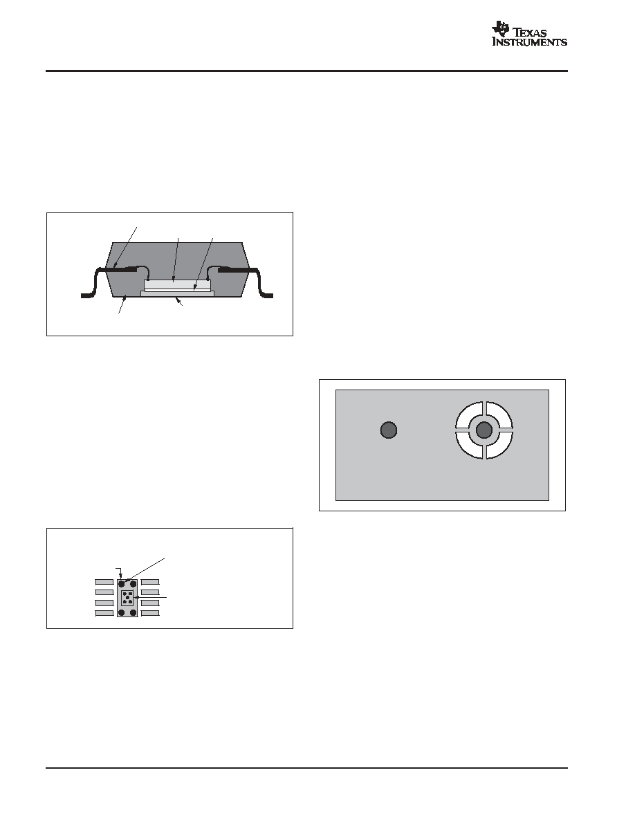
The PowerPAD package is designed so that the leadframe
die pad (or thermal pad) is exposed on the bottom of the
IC, as shown in Figure 9. This provides an extremely low
thermal resistance (
q
JC
) path between the die and the
exterior of the package. The thermal pad on the bottom of
the IC can then be soldered directly to the PCB, using the
PCB as a heatsink. In addition, plated-through holes (vias)
provide a low thermal resistance heat flow path to the back
side of the PCB.
Mold Compound (Plastic)
Leadframe Die Pad
Exposed at Base of the Package
(Copper Alloy)
Leadframe (Copper Alloy)
IC (Silicon)
Die Attach (Epoxy)
Figure 9. Section View of a PowerPAD Package
PowerPAD ASSEMBLY PROCESS
1. The PowerPAD must be connected to the device's most
negative supply voltage, which will be ground in
single-supply applications, and V- in split-supply
applications.
2. Prepare the PCB with a top-side etch pattern, as shown
in Figure 10. The exact land design may vary based on the
specific assembly process requirements. There should be
etch for the leads as well as etch for the thermal land.
OPTIONAL:
Additional 4 vias outside
of thermal pad area but
under the package.
REQUIRED:
Thermal pad area 2.286mm x 2.286mm
(90 mils x 90 mils) with 5 vias
(via diameter = 13 mils)
Thermal Land
(Copper)
Minimum Size
4.8mm x 3.8mm
(189 mils x 150 mils)
Figure 10. 8-Pin PowerPAD PCB Etch and Via
Pattern
3. Place the recommended number of plated-through
holes (or thermal vias) in the area of the thermal pad.
These holes should be 13 mils in diameter. They are kept
small so that solder wicking through the holes is not a
problem during reflow. The minimum recommended
number of holes for the SO-8 PowerPAD package is 5, as
shown in Figure 10.
4. It is recommended, but not required, to place a small
number of additional holes under the package and outside
the thermal pad area. These holes provide additional heat
paths between the copper thermal land and the ground
plane. They may be larger because they are not in the area
to be soldered, so wicking is not a problem. This is
illustrated in Figure 10.
5. Connect all holes, including those within the thermal pad
area and outside the pad area, to the internal ground plane
or other internal copper plane for single-supply
applications, and to V- for split-supply applications.
6. When laying out these holes, do not use the typical web
or spoke via connection methodology, as shown in
Figure
11. Web connections have a high thermal
resistance connection that is useful for slowing the heat
transfer during soldering operations. This makes soldering
the vias that have ground plane connections easier.
However, in this application, low thermal resistance is
desired for the most efficient heat transfer. Therefore, the
holes under the PowerPAD package should make their
connection to the internal ground plane with a complete
connection around the entire circumference of the
plated-through hole.
Web or Spoke Via
Solid Via
NOT RECOMMENDED
(due to poor heat conduction)
RECOMMENDED
Figure 11. Via Connection
7. The top-side solder mask should leave the pad
connections and the thermal pad area exposed. The
thermal pad area should leave the 13 mil holes exposed.
The larger holes outside the thermal pad area may be
covered with solder mask.
8. Apply solder paste to the exposed thermal pad area and
all of the package terminals.
9. With these preparatory steps in place, the PowerPAD IC
is simply placed in position and run through the solder
reflow operation as any standard surface-mount
component. This results in a part that is properly installed.
For detailed information on the PowerPAD package
including thermal modeling considerations and repair
procedures, please see Technical Brief SLMA002,
PowerPAD Thermally Enhanced Package, located at
www.ti.com.

PACKAGING INFORMATION
ORDERABLE DEVICE
STATUS(1)
PACKAGE TYPE
PACKAGE DRAWING
PINS
PACKAGE QTY
OPA2354AIDDA
ACTIVE
HSOP
DDA
8
100
OPA2354AIDDAR
ACTIVE
HSOP
DDA
8
2500
OPA2354AIDGKR
ACTIVE
VSSOP
DGK
8
2500
OPA2354AIDGKT
ACTIVE
VSSOP
DGK
8
250
OPA354AIDBVR
ACTIVE
SOP
DBV
5
3000
OPA354AIDBVT
ACTIVE
SOP
DBV
5
250
OPA354AIDDA
ACTIVE
HSOP
DDA
8
100
OPA354AIDDAR
ACTIVE
HSOP
DDA
8
2500
OPA4354AID
ACTIVE
SOIC
D
14
58
OPA4354AIDR
ACTIVE
SOIC
D
14
2500
OPA4354AIPWR
ACTIVE
TSSOP
PW
14
2500
OPA4354AIPWT
ACTIVE
TSSOP
PW
14
250
(1) The marketing status values are defined as follows:
ACTIVE: Product device recommended for new designs.
LIFEBUY: TI has announced that the device will be discontinued, and a lifetime-buy period is in effect.
NRND: Not recommended for new designs. Device is in production to support existing customers, but TI does not recommend using this part in
a new design.
PREVIEW: Device has been announced but is not in production. Samples may or may not be available.
OBSOLETE: TI has discontinued the production of the device.
PACKAGE OPTION ADDENDUM
www.ti.com
21-May-2004


MECHANICAL DATA
MTSS001C JANUARY 1995 REVISED FEBRUARY 1999
POST OFFICE BOX 655303
·
DALLAS, TEXAS 75265
PW (R-PDSO-G**)
PLASTIC SMALL-OUTLINE PACKAGE
14 PINS SHOWN
0,65
M
0,10
0,10
0,25
0,50
0,75
0,15 NOM
Gage Plane
28
9,80
9,60
24
7,90
7,70
20
16
6,60
6,40
4040064/F 01/97
0,30
6,60
6,20
8
0,19
4,30
4,50
7
0,15
14
A
1
1,20 MAX
14
5,10
4,90
8
3,10
2,90
A MAX
A MIN
DIM
PINS **
0,05
4,90
5,10
Seating Plane
0
°
8
°
NOTES: A. All linear dimensions are in millimeters.
B. This drawing is subject to change without notice.
C. Body dimensions do not include mold flash or protrusion not to exceed 0,15.
D. Falls within JEDEC MO-153

IMPORTANT NOTICE
Texas Instruments Incorporated and its subsidiaries (TI) reserve the right to make corrections, modifications,
enhancements, improvements, and other changes to its products and services at any time and to discontinue
any product or service without notice. Customers should obtain the latest relevant information before placing
orders and should verify that such information is current and complete. All products are sold subject to TI's terms
and conditions of sale supplied at the time of order acknowledgment.
TI warrants performance of its hardware products to the specifications applicable at the time of sale in
accordance with TI's standard warranty. Testing and other quality control techniques are used to the extent TI
deems necessary to support this warranty. Except where mandated by government requirements, testing of all
parameters of each product is not necessarily performed.
TI assumes no liability for applications assistance or customer product design. Customers are responsible for
their products and applications using TI components. To minimize the risks associated with customer products
and applications, customers should provide adequate design and operating safeguards.
TI does not warrant or represent that any license, either express or implied, is granted under any TI patent right,
copyright, mask work right, or other TI intellectual property right relating to any combination, machine, or process
in which TI products or services are used. Information published by TI regarding third-party products or services
does not constitute a license from TI to use such products or services or a warranty or endorsement thereof.
Use of such information may require a license from a third party under the patents or other intellectual property
of the third party, or a license from TI under the patents or other intellectual property of TI.
Reproduction of information in TI data books or data sheets is permissible only if reproduction is without
alteration and is accompanied by all associated warranties, conditions, limitations, and notices. Reproduction
of this information with alteration is an unfair and deceptive business practice. TI is not responsible or liable for
such altered documentation.
Resale of TI products or services with statements different from or beyond the parameters stated by TI for that
product or service voids all express and any implied warranties for the associated TI product or service and
is an unfair and deceptive business practice. TI is not responsible or liable for any such statements.
Following are URLs where you can obtain information on other Texas Instruments products and application
solutions:
Products
Applications
Amplifiers
amplifier.ti.com
Audio
www.ti.com/audio
Data Converters
dataconverter.ti.com
Automotive
www.ti.com/automotive
DSP
dsp.ti.com
Broadband
www.ti.com/broadband
Interface
interface.ti.com
Digital Control
www.ti.com/digitalcontrol
Logic
logic.ti.com
Military
www.ti.com/military
Power Mgmt
power.ti.com
Optical Networking
www.ti.com/opticalnetwork
Microcontrollers
microcontroller.ti.com
Security
www.ti.com/security
Telephony
www.ti.com/telephony
Video & Imaging
www.ti.com/video
Wireless
www.ti.com/wireless
Mailing Address:
Texas Instruments
Post Office Box 655303 Dallas, Texas 75265
Copyright
2004, Texas Instruments Incorporated