
PRODUCTION DATA information is current as of publication date.
Products conform to specifications per the terms of Texas Instruments
standard warranty. Production processing does not necessarily include
testing of all parameters.
OPA2822
SBOS188C MARCH 2001 REVISED MAY 2004
DESCRIPTION
The OPA2822 offers very low 2.0nV/
Hz input noise in a
wideband, unity-gain stable, voltage-feedback architecture.
Intended for xDSL receiver applications, the OPA2822 also
supports this low input noise with exceptionally low harmonic
distortion, particularly in differential configurations. Adequate
output current is provided to drive the potentially heavy load
of a passive filter between this amplifier and the codec.
Harmonic distortion for a 2V
PP
differential output operating
from +5V to +12V supplies is
100dBc through 1MHz input
frequencies. Operating on a low 4.8mA/ch supply current,
the OPA2822 can satisfy all xDSL receiver requirements
over a wide range of possible supply voltages--from a single
+5V condition, to
±
5V, up to a single +12V design.
General-purpose applications on a single +5V supply will
benefit from the high input and output voltage swing available
on this reduced supply voltage. Low-cost precision integra-
tors for PLLs will also benefit from the low voltage noise and
offset voltage. Baseband I/Q receiver channels can achieve
almost perfect channel match with noise and distortion to
support signals through 5MHz with > 14-bit dynamic range.
FEATURES
q
LOW INPUT NOISE VOLTAGE: 2.0nV/
Hz
q
HIGH UNITY GAIN BANDWIDTH: 500MHz
q
HIGH GAIN BANDWIDTH PRODUCT: 240MHz
q
HIGH OUTPUT CURRENT: 90mA
q
SINGLE +5V TO +12V OPERATION
q
LOW SUPPLY CURRENT: 4.8mA/ch
Dual, Wideband, Low-Noise
Operational Amplifier
APPLICATIONS
q
xDSL DIFFERENTIAL LINE RECEIVERS
q
HIGH DYNAMIC RANGE ADC DRIVERS
q
LOW NOISE PLL INTEGRATORS
q
TRANSIMPEDANCE AMPLIFIERS
q
PRECISION BASEBAND I/Q AMPLIFIERS
q
ACTIVE FILTERS
FEATURES
SINGLES
DUALS
TRIPLES
High Slew Rate
OPA690
OPA2690
OPA3690
R/R Input/Output
OPA353
OPA2353
--
1.3nV Input Noise
OPA846
OPA2686
--
1.5nV Input Noise
--
THS6062
--
OPA2822 RELATED PRODUCTS
xDSL Driver
OPA2677
xDSL Receiver
500
500
500
R
O
OPA2822
OPA2822
1k
500
n:1
1k
R
O
OPA2
822
www.ti.com
Copyright © 2001-2004, Texas Instruments Incorporated
All trademarks are the property of their respective owners.
Please be aware that an important notice concerning availability, standard warranty, and use in critical applications of
Texas Instruments semiconductor products and disclaimers thereto appears at the end of this data sheet.

OPA2822
2
SBOS188C
www.ti.com
Supply Voltage .................................................................................
±
6.5V
Internal Power Dissipation ........................... See Thermal Characteristics
Differential Input Voltage ..................................................................
±
1.2V
Input Voltage Range ............................................................................
±
V
S
Storage Temperature Range ......................................... 40
°
C to +125
°
C
Lead Temperature (SO-8) ............................................................. +260
°
C
Junction Temperature (T
J
) ........................................................... +150
°
C
ESD Rating (Human Body Model) .................................................. 2000V
(Machine Model) ........................................................... 200V
NOTE: (1) Stresses above these ratings may cause permanent damage.
Exposure to absolute maximum conditions for extended periods may degrade
device reliability. These are stress ratings only, and functional operation of the
device at these or any other conditions beyond those specified is not implied.
ABSOLUTE MAXIMUM RATINGS
(1)
PACKAGE/ORDERING INFORMATION
(1)
SPECIFIED
PACKAGE
TEMPERATURE
PACKAGE
ORDERING
TRANSPORT
PRODUCT
PACKAGE-LEAD
DESIGNATOR
RANGE
MARKING
NUMBER
MEDIA, QUANTITY
OPA2822U
SO-8 Surface-Mount
D
40
°
C to +85
°
C
OPA2822U
OPA2822U
Rails, 100
"
"
"
"
"
OPA2822U/2K5
Tape and Reel, 2500
OPA2822E
MSOP-8 Surface-Mount
DGK
40
°
C to +85
°
C
D22
OPA2822E/250
Tape and Reel, 250
"
"
"
"
"
OPA2822E/2K5
Tape and Reel, 2500
NOTE: (1) For the most current package and ordering information, see the Package Option Addendum located at the end of this data sheet.
ELECTROSTATIC
DISCHARGE SENSITIVITY
Electrostatic discharge can cause damage ranging from per-
formance degradation to complete device failure. Texas In-
struments recommends that all integrated circuits be handled
and stored using appropriate ESD protection methods.
ESD damage can range from subtle performance degradation
to complete device failure. Precision integrated circuits may be
more susceptible to damage because very small parametric
changes could cause the device not to meet published speci-
fications.
Top View
SO
PIN CONFIGURATION / MSOP PACKING MARKING
MSOP PACKAGE MARKING
1
2
3
4
8
7
6
5
+V
S
Out B
In B
+In B
Out A
In A
+In A
V
S
OPA2822
D22
8
7
6
5
1
2
3
4

OPA2822
3
SBOS188C
www.ti.com
AC PERFORMANCE (see Figure 1)
Small-Signal Bandwidth
G = +1, V
O
= 0.1V
PP
, R
F
= 0
400
MHz
typ
C
G = +2, V
O
= 0.1V
PP
200
120
110
105
MHz
min
B
G = +10, V
O
= 0.1V
PP
24
15
13
12
MHz
min
B
Gain-Bandwidth Product
G
20
240
150
130
125
MHz
min
B
Bandwidth for 0.1dB Gain Flatness
G = +2, V
O
< 0.1V
PP
16
MHz
typ
C
Peaking at a Gain of +1
V
O
< 0.1V
PP
5
dB
typ
C
Large-Signal Bandwidth
G = +2, V
O
= 2V
PP
27
MHz
typ
C
Slew Rate
G = +2, 4V Step
170
110
105
100
V/
µ
s
min
B
Rise-and-Fall Time
G = +2, V
O
= 0.2V Step
1.5
ns
typ
C
Settling Time to 0.02%
G = +2, V
O
= 2V Step
35
ns
typ
C
0.1%
G = +2, V
O
= 2V Step
32
ns
typ
C
Harmonic Distortion
G = +2, f = 1MHz, V
O
= 2V
PP
2nd-Harmonic
R
L
= 200
91
88
87
86
dBc
max
B
R
L
500
95
91
90
89
dBc
max
B
3rd-Harmonic
R
L
= 200
100
95
92
91
dBc
max
B
R
L
500
105
99
96
95
dBc
max
B
Input Voltage Noise
f > 10kHz
2.0
2.2
2.3
2.5
nV/
Hz
max
B
Input Current Noise
f > 10kHz
1.6
2.0
2.1
2.3
pA/
Hz
max
B
Differential Gain
G = +2, PAL, V
O
= 1.4Vp, R
L
= 150
0.02
%
typ
C
Differential Phase
G = +2, PAL, V
O
= 1.4Vp, R
L
= 150
0.03
deg
typ
C
Channel-to-Channel Crosstalk
f = 1MHz, Input Referred
95
dBc
typ
C
DC PERFORMANCE
(4)
Open-Loop Voltage Gain (A
OL
)
V
O
= 0V, R
L
= 100
100
85
82
80
dB
min
A
Input Offset Voltage
V
CM
= 0V
±
0.2
±
1.2
±
1.4
±
1.5
mV
max
A
Average Offset Voltage Drift
V
CM
= 0V
5
5
µ
V/
°
C
max
B
Input Bias Current
V
CM
= 0V
9
18
19
21
µ
A
max
A
Average Bias Current Drift (magnitude)
V
CM
= 0V
50
50
nA/
°
C
max
B
Input Offset Current
V
CM
= 0V
±
100
±
400
±
600
±
700
nA
max
A
Average Offset Current Drift
V
CM
= 0V
5
5
nA/
°
C
max
B
INPUT
Common-Mode Input Range (CMIR)
(5)
±
4.8
±
4.5
±
4.4
±
4.4
V
min
A
Common-Mode Rejection Ratio (CMRR)
V
CM
=
±
1V
110
85
82
80
dB
min
A
Input Impedance
Differential-Mode
V
CM
= 0
18
0.6
k
|| pF
typ
C
Common-Mode
V
CM
= 0
7
1
M
|| pF
typ
C
OUTPUT
Voltage Output Swing
No Load
±
4.9
±
4.7
±
4.6
±
4.6
V
min
A
100
Load
±
4.7
±
4.5
±
4.4
±
4.4
V
min
A
Current Output, Sourcing
V
O
= 0, Linear Operation
+150
+90
+85
+80
mA
min
A
Current Output, Sinking
V
O
= 0, Linear Operation
150
90
85
80
mA
min
A
Short-Circuit Current
Output Shorted to Ground
220
mA
typ
C
Closed-Loop Output Impedance
G = +2, f = 100kHz
0.01
typ
C
POWER SUPPLY
Specified Operating Voltage
±
6
V
typ
C
Maximum Operating Voltage Range
±
6.3
±
6.3
±
6.3
V
max
A
Max Quiescent Current
V
S
=
±
6V, both channels
9.6
11.8
11.9
12.0
mA
max
A
Min Quiescent Current
V
S
=
±
6V, both channels
9.6
8.2
8.1
8.0
mA
min
A
Power-Supply Rejection Ratio (PSRR)
Input Referred
95
85
82
80
dB
min
A
THERMAL CHARACTERISTICS
Specified Operating Range U, E Package
40 to +85
°
C
typ
C
Thermal Resistance,
JA
Junction-to-Ambient
U
SO-8
125
°
C/W
typ
C
E
MSOP
150
°
C/W
typ
C
NOTES: (1) Junction temperature = ambient for +25
°
C tested specifications.
(2) Junction temperature = ambient at low temperature limit: junction temperature = ambient +23
°
C at high temperature limit for over temperature tested
specifications.
(3) Test Levels: (A) 100% tested at +25
°
C. Over temperature limits by characterization and simulation. (B) Limits set by characterization and simulation. (C)
Typical value only for information.
(4) Current is considered positive-out-of node. V
CM
is the input common-mode voltage.
(5) Tested < 3dB below minimum CMRR specification at
±
CMIR limits.
ELECTRICAL CHARACTERISTICS: V
S
=
±
6V
Boldface limits are tested at +25
°
C.
R
F
= 402
, R
L
= 100
, and G = +2
,
(see Figure 1 for AC performance only), unless otherwise noted.
OPA2822U, E
TYP
MIN/MAX OVER TEMPERATURE
0
°
C to
40
°
C to
MIN/
TEST
PARAMETER
CONDITIONS
+25
°
C
+25
°
C
(1)
70
°
C
(2)
+85
°
C
(2)
UNITS
MAX
LEVEL
(3)

OPA2822
4
SBOS188C
www.ti.com
AC PERFORMANCE (see Figure 3)
Small-Signal Bandwidth
G = +1, V
O
= 0.1V
PP
, R
F
= 0
350
MHz
typ
C
G = +2, V
O
= 0.1V
PP
180
105
102
100
MHz
min
B
G = +10, V
O
= 0.1V
PP
20
13
11
10
MHz
min
B
Gain-Bandwidth Product
G > 20
200
130
110
105
MHz
min
B
Peaking at a Gain of +1
V
O
< 0.1V
PP
6
dB
typ
C
Large-Signal Bandwidth
G = +2, V
O
= 2V
PP
20
MHz
typ
C
Slew Rate
G = +2, 2V Step
120
90
85
80
V/
µ
s
min
B
Rise-and-Fall Time
G = +2, V
O
= 0.2V Step
2.0
2.7
3.2
3.3
ns
max
B
Settling Time to 0.02%
G = +2, V
O
= 2V Step
40
ns
typ
C
0.1%
G = +2, V
O
= 2V Step
38
ns
typ
C
Harmonic Distortion
G = +2, f = 1MHz, V
O
= 2V
PP
2nd-Harmonic
R
L
= 200
to V
S
/ 2
85
82
81
80
dBc
max
B
R
L
= 500
to V
S
/ 2
87
83
82
81
dBc
max
B
3rd-Harmonic
R
L
= 100
to V
S
/ 2
99
94
91
90
dBc
max
B
R
L
= 1500
to V
S
/2
103
98
95
94
dBc
max
B
Input Voltage Noise
f > 1MHz
2.1
2.3
2.4
2.6
nV/
Hz
max
B
Input Current Noise
f > 1MHz
1.5
1.9
2.0
2.1
pA/
Hz
max
B
DC PERFORMANCE
(4)
Open-Loop Voltage Gain
V
O
= 0V, R
L
= 200
to 2.5V
90
81
78
76
dB
min
A
Input Offset Voltage
V
CM
= 2.5V
±
0.3
±
1.3
±
1.5
±
1.6
mV
max
A
Average Offset Voltage Drift
V
CM
= 2.5V
5.5
5.5
µ
V/
°
C
max
B
Input Bias Current
V
CM
= 2.5V
8
16
19
20
µ
A
max
A
Average Bias Current Drift
V
CM
= 2.5V
50
50
nA/
°
C
max
B
Input Offset Current
V
CM
= 2.5V
±
100
±
400
±
600
±
700
nA
max
A
Average Offset Current Drift
V
CM
= 2.5V
5
5
nA/
°
C
max
B
INPUT
Least Positive Input Voltage
1.2
1.5
1.6
1.65
V
min
A
Most Positive Input Voltage
3.8
3.5
3.4
3.35
V
max
A
Common-Mode Rejection Ratio (CMRR)
V
CM
= +2.5V
110
85
82
80
dB
min
A
Input Impedance
Differential-Mode
V
CM
= +2.5V
15
1
k
|| pF
typ
C
Common-Mode
V
CM
= +2.5V
5
1.3
M
|| pF
typ
C
OUTPUT
Most Positive Output Voltage
No Load
3.9
3.8
3.6
3.5
V
min
A
R
L
= 100
to 2.5V
3.7
3.5
3.4
3.35
V
min
A
Least Positive Output Voltage
No Load
1.3
1.4
1.5
1.55
V
min
A
R
L
= 100
to 2.5V
1.4
1.5
1.6
1.65
V
min
A
Current Output, Sourcing
+150
+90
+85
+80
mA
min
A
Current Output, Sinking
150
90
85
80
mA
min
A
Short-Circuit Current
Output Shorted to Either Supply
200
mA
typ
C
Closed-Loop Output Impedance
G = +1, f = 100kHz
0.01
typ
C
POWER SUPPLY
Specified Single-Supply Operating Voltage
5
V
typ
C
Maximum Single-Supply Operating Voltage
12.6
12.6
12.6
V
max
A
Max Quiescent Current
V
S
= +5V, both channels
8
10
10.2
10.4
mA
max
A
Min Quiescent Current
V
S
= +5V, both channels
8
7.2
7.0
6.9
mA
min
A
Power-Supply Rejection Ratio
Input Referred
90
dB
typ
C
THERMAL CHARACTERISTICS
Specified Operating Range U, E Package
40 to +85
°
C
typ
C
Thermal Resistance,
JA
Junction-to-Ambient
U
SO-8
125
°
C/W
typ
C
E
MSOP
150
°
C/W
typ
C
NOTES: (1) Junction temperature = ambient for +25
°
C tested specifications.
(2) Junction temperature = ambient at low temperature limit: junction temperature = ambient +23
°
C at high temperature limit for over temperature tested
specifications.
(3) Test Levels: (A) 100% tested at +25
°
C. Over temperature limits by characterization and simulation. (B) Limits set by characterization and simulation.
(C) Typical value only for information.
(4) Current is considered positive-out-of node. V
CM
is the input common-mode voltage.
ELECTRICAL CHARACTERISTICS: V
S
= +5V
Boldface limits are tested at +25
°
C.
R
F
= 402
, R
L
= 100
to V
S
/ 2, and G = +2
,
(see Figure 3 for AC performance only), unless otherwise noted.
OPA2822U, E
TYP
MIN/MAX OVER TEMPERATURE
0
°
C to
40
°
C to
MIN/
TEST
PARAMETER
CONDITIONS
+25
°
C
+25
°
C
(1)
70
°
C
(2)
+85
°
C
(2)
UNITS
MAX
LEVEL
(3)

OPA2822
5
SBOS188C
www.ti.com
TYPICAL CHARACTERISTICS: V
S
=
±
6V
T
A
= +25
°
C, G
= +2, R
F
= 402
, and R
L
= 100
, unless otherwise noted.
6
3
0
3
6
9
12
15
18
21
24
NONINVERTING SMALL-SIGNAL
FREQUENCY RESPONSE
Frequency (MHz)
0.5
1
10
100
500
Normalized Gain (dB)
G = +1
R
F
= 0
G = +2
G = +5
G = +10
V
O
= 0.1V
PP
See Figure 1
6
3
0
3
6
9
12
15
18
21
24
INVERTING SMALL-SIGNAL
FREQUENCY RESPONSE
Frequency (MHz)
0.5
1
10
100
500
Normalized Gain (dB)
G = 1
G = 10
G = 5
V
O
= 0.1V
PP
R
F
= 604
See Figure 2
G = 2
NONINVERTING LARGE-SIGNAL
FREQUENCY RESPONSE
Frequency (MHz)
0.5
1
10
100
500
Gain (dB)
12
9
6
3
0
3
6
9
12
15
18
G = +2
V
O
= 0.1V
PP
V
O
= 0.5V
PP
V
O
= 1V
PP
V
O
= 2V
PP
See Figure 1
6
3
0
3
6
9
12
15
18
21
24
INVERTING LARGE-SIGNAL
FREQUENCY RESPONSE
Frequency (MHz)
0.5
1
10
100
500
Gain (dB)
G = 1
R
F
= 604
V
O
= 0.1V
PP
V
O
= 0.5V
PP
V
O
= 1V
PP
V
O
= 2V
PP
See Figure 2
400
300
200
100
0
100
200
300
400
NONINVERTING PULSE RESPONSE
Time (20ns/div)
Small-Signal Output Voltage (100mv/div)
2.0
1.5
1.0
0.5
0
0.5
1.0
1.5
2.0
Larege-Signal Output Voltage (500mv/div)
See Figure 1
Large-Signal Right Scale
Small-Signal Left Scale
G = +2
400
300
200
100
0
100
200
300
400
INVERTING PULSE RESPONSE
Time (20ns/div)
Small-Signal Output Voltage (100mv/div)
2.0
1.5
1.0
0.5
0
0.5
1.0
1.5
2.0
Larege-Signal Output Voltage (500mv/div)
See Figure 2
Large-Signal Right Scale
Small-Signal Left Scale
G = 1
OPA2822
6
SBOS188C
www.ti.com
TYPICAL CHARACTERISTICS: V
S
=
±
6V
(Cont.)
T
A
= +25
°
C, G
= +2, R
F
= 402
, and R
L
= 100
, unless otherwise noted.
85
90
95
100
105
HARMONIC DISTORTION vs LOAD RESISTANCE
Load Resistance (
)
100
1k
Harmonic Distortion (dBc)
V
O
= 2V
PP
f = 1MHz
2nd-Harmonic
3rd-Harmonic
See Figure 1
1MHz HARMONIC DISTORTION vs SUPPLY VOLTAGE
Supply Voltage (V)
±
2.5
±
3.0
±
3.5
±
4.0
±
4.5
±
5.0
±
5.5
±
6.0
Harmonic Distortion (dBc)
85
90
95
100
105
2nd-Harmonic
3rd-Harmonic
See Figure 1
V
O
= 2V
PP
R
L
= 200
65
75
85
95
105
HARMONIC DISTORTION vs FREQUENCY
Frequency (MHz)
1
10
Harmonic Distortion (dBc)
V
O
= 2V
PP
R
L
= 200
2nd-Harmonic
3rd-Harmonic
See Figure 1
HARMONIC DISTORTION vs OUTPUT VOLTAGE
Output Voltage Swing (V
PP
)
0.1
1
10
Harmonic Distortion (dBc)
85
90
95
100
105
R
L
= 200
f = 1MHz
2nd-Harmonic
3rd-Harmonic
See Figure 1
70
80
90
100
110
HARMONIC DISTORTION vs NONINVERTING GAIN
Gain (V/V)
1
10
Harmonic Distortion (dBc)
V
O
= 2V
PP
R
L
= 200
f = 1MHz
2nd-Harmonic
3rd-Harmonic
See Figure 1
70
80
90
100
110
HARMONIC DISTORTION vs INVERTING GAIN
Gain (V/V)
1
10
Harmonic Distortion (dBc)
3rd-Harmonic
See Figure 2
V
O
= 2V
PP
R
L
= 200
R
F
= 604
f = 1MHz
2nd-Harmonic
OPA2822
7
SBOS188C
www.ti.com
TYPICAL CHARACTERISTICS: V
S
=
±
6V
(Cont.)
T
A
= +25
°
C, G
= +2, R
F
= 402
, and R
L
= 100
, unless otherwise noted.
INPUT VOLTAGE AND CURRENT NOISE DENSITY
Frequency (Hz)
10
2
10
4
10
5
10
6
10
3
10
7
Voltage Noise nV/
Hz
Current Noise pA/
Hz
10
1
2nV/
Hz
1.6pA/
Hz
Voltage Noise
Current Noise
2-TONE, 3rd-ORDER
INTERMODULATION INTERCEPT
Frequency (MHz)
1
10
20
Intercept Point (+dBm)
60
55
50
45
40
35
30
25
20
1/2
OPA2822
50
50
P
I
50
402
402
P
O
CHANNEL-TO-CHANNEL CROSSTALK
Frequency (MHz)
0.1
100
10
1
500
Cross-Talk Input Referred (dB)
40
50
60
70
80
90
100
Input Referred
R
L
= 100
G = +2
GAIN FLATNESS
Frequency (MHz)
0
150
100
50
200
Deviation from 6dB Gain (0.1dB/div)
0.50
0.40
0.30
0.20
0.10
0.00
0.10
0.20
0.30
0.40
0.50
NG = 3.5
R
NG
= 301
NG = 3.0
R
NG
= 452
NG = 2.5
R
NG
= 904
G = 2
Noise Gain
Adjusted
See Figure 12
NG = 2
R
NG
=
RECOMMENDED R
S
vs CAPACITIVE LOAD
Capacitive Load (pF)
10
100
1k
R
S
(
)
1000
100
10
1
For Maximally Flat Response,
See Figure 12
FREQUENCY RESPONSE vs CAPACITIVE LOAD
Frequency (MHz)
1
10
100
500
Normalized Gain to Capacitive Load (dB)
9
6
3
0
3
6
9
12
1/2
OPA2822
R
S
V
I
1k
1k
is optional.
C
L
402
402
V
O
C
L
= 100pF
C
L
= 10pF
C
L
= 22pF
C
L
= 47pF
OPA2822
8
SBOS188C
www.ti.com
TYPICAL CHARACTERISTICS: V
S
=
±
6V
(Cont.)
T
A
= +25
°
C, G
= +2, R
F
= 402
, and R
L
= 100
, unless otherwise noted.
CMRR AND PSRR vs FREQUENCY
Frequency (Hz)
10
3
10
4
10
5
10
6
10
7
10
8
Common-Mode Rejection Ratio (dB)
Power-Supply Rejection Ratio (dB)
120
100
80
60
40
20
0
CMRR
+PSRR
PSRR
OPEN-LOOP GAIN AND PHASE
Frequency (Hz)
10
2
10
3
10
4
10
5
10
6
10
7
10
8
10
9
Open-Loop Gain (dB)
120
100
80
60
40
20
0
20
Open-Loop Phase (30
°
/div)
0
30
60
90
120
150
180
210
20 log(A
OL
)
A
OL
OUTPUT VOLTAGE AND CURRENT LIMITATIONS
I
O
(mA)
200
150
100
50
0
50
100
150
200
V
O
(V)
6
5
4
3
2
1
0
1
2
3
4
5
6
1W Internal
Power Limit
Single-Channel
1W Internal
Power Limit
Single-Channel
R
L
= 25
R
L
= 100
R
L
= 50
CLOSED-LOOP OUTPUT IMPEDANCE
vs FREQUENCY
Frequency (MHz)
0.1
1
10
100
Output Impedance (
)
10
1
10
0.1
0.01
0.001
1/2
OPA2822
402
402
Z
O
8
6
4
2
0
2
4
6
8
NONINVERTING OVERDRIVE RECOVERY
Time (40ns/div)
Output Voltage
4
3
2
1
0
1
2
3
4
Input Voltage
R
L
= 100
G = +2
See Figure 1
Output
Left Scale
Input Right Scale
8
6
4
2
0
2
4
6
8
INVERTING OVERDRIVE RECOVERY
Time (40ns/div)
Input/Output Voltage
R
L
= 100
R
F
= 604
G = 1
See Figure 2
Output
Input
OPA2822
9
SBOS188C
www.ti.com
TYPICAL CHARACTERISTICS: V
S
=
±
6V
(Cont.)
T
A
= +25
°
C, G
= +2, R
F
= 402
, and R
L
= 100
, unless otherwise noted.
SETTLING TIME
Time (ns)
0
20
15
10
5
40
45
50
55
25
30
35
60
Percent of Final Value (%)
0.25
0.20
0.15
0.10
0.05
0
0.05
0.10
0.15
0.20
0.25
See Figure 1
R
L
= 100
V
O
= 2V step
G = +2
VIDEO DIFFERENTIAL GAIN/DIFFERENTIAL PHASE
Video Loads
dP
dG
1
2
3
4
5
6
7
8
Differential Gain (%)
Differential Phase (
°
)
0.30
0.25
0.20
0.15
0.10
0.05
0
TYPICAL DC DRIFT OVER TEMPERATURE
Ambient Temperature (
°
C)
50
25
0
25
50
75
100
125
Input Offset Voltage (mV)
1
0.5
0
0.5
1
Input Bias and Offset Current (
µ
A)
10
5
0
5
10
Input Offset Voltage
10x Input Offset Current
Input Bias Current
SUPPLY AND OUTPUT CURRENT
vs TEMPERATURE
Ambient Temperature (
°
C)
50
25
0
25
50
75
100
125
Output Current (25mA/div)
250
225
200
175
150
125
100
Supply Current (1mA/div)
12
11
10
9
8
7
6
Sourcing Output Current
Left Scale
Current Limited Output
Sinking Output
Current
Left Scale
Supply Current
(both channels)
Right Scale
COMMON-MODE INPUT RANGE AND
OUTPUT SWING vs SUPPLY VOLTAGE
Supply Voltage (
±
V)
±
2
±
3
±
4
±
5
±
6
Voltage Range (V)
6
4
2
0
2
4
6
Positive Input
and Output
Negative Input
and Output
COMMON-MODE AND DIFFERENTIAL
INPUT IMPEDANCE
Frequency (Hz)
10
3
10
4
10
5
10
6
10
7
10
8
Input Impedance Magnitude 20Log (
) 10
7
10
6
10
5
10
4
10
3
10
2
Common-Mode
Differential
OPA2822
10
SBOS188C
www.ti.com
TYPICAL CHARACTERISTICS: V
S
=
±
6V
T
A
= +25
°
C, Differential Gain
= 2, R
F
= 604
, and R
L
= 400
, unless otherwise noted.
1/2
OPA2822
R
G
604
+6V
1/2
OPA2822
R
G
R
L
V
I
604
V
O
6V
G
D =
604
R
G
6
3
0
3
6
9
12
15
18
21
24
DIFFERENTIAL SMALL-SIGNAL
FREQUENCY RESPONSE
Frequency (MHz)
0.5
1
10
100
500
Normalized Gain (dB)
G
D
= +1
G
D
= +2
G
D
= +5
G
D
= +10
V
O
= 200mV
PP
12
9
6
3
0
3
6
9
12
15
18
DIFFERENTIAL LARGE-SIGNAL
FREQUENCY RESPONSE
Frequency (MHz)
0.5
1
10
100
500
Gain (dB)
V
O
= 200mV
PP
V
O
= 1V
PP
V
O
= 2V
PP
G
D
= 2
R
L
= 400
V
O
= 5V
PP
DIFFERENTIAL DISTORTION vs LOAD RESISTANCE
Load Resistance (
)
10
100
1k
Harmonic Distortion (dBc)
85
90
95
100
105
V
O
= 4V
PP
G
D
= 2
f = 1MHz
2nd-Harmonic
3rd-Harmonic
65
75
85
95
105
DIFFERENTIAL DISTORTION vs FREQUENCY
Frequency (MHz)
1
10
Harmonic Distortion (dBc)
2nd-Harmonic
3rd-Harmonic
V
O
= 4V
PP
G
D
= 2
R
L
= 400
95
100
105
110
115
DIFFERENTIAL DISTORTION vs OUTPUT VOLTAGE
Differential Output Voltage Swing (V
PP
)
1
10
Harmonic Distortion (dBc)
2nd-Harmonic
3rd-Harmonic
f = 1MHz
G
D
= 2
R
L
= 400
DIFFERENITAL PERFORMANCE
TEST CIRCUIT

OPA2822
11
SBOS188C
www.ti.com
TYPICAL CHARACTERISTICS: V
S
= +5V
T
A
= +25
°
C, G
= +2, R
F
= 402
, and R
L
= 100
, unless otherwise noted.
9
6
3
0
3
6
9
12
15
18
21
24
NONINVERTING SMALL-SIGNAL
FREQUENCY RESPONSE
Frequency (MHz)
0.5
1
10
100
500
Normalized Gain (dB)
V
O
= 0.1V
PP
G = +1
R
F
= 0
G = +2
See Figure 3
G = +5
G = +10
6
3
0
3
6
9
12
15
18
21
24
INVERTING SMALL-SIGNAL
FREQUENCY RESPONSE
Frequency (MHz)
0.5
1
10
100
500
Normalized Gain (dB)
V
O
= 0.1V
PP
R
F
= 604
See Figure 4
G = 5
G = 2
G = 1
G = 10
0.4
0.3
0.2
0.1
0
0.1
0.2
0.3
0.4
NONINVERTING PULSE RESPONSE
Time (20ns/div)
Small-Signal Output Voltage (100mv/div)
2.0
1.5
1.0
0.5
0
0.5
1.0
1.5
2.0
Large-Signal Output Voltage (500mv/div)
See Figure 3
Large-Signal Right Scale
Small-Signal Left Scale
0.4
0.3
0.2
0.1
0
0.1
0.2
0.3
0.4
INVERTING PULSE RESPONSE
Time (20ns/div)
Small-Signal Output Voltage (100mv/div)
2.0
1.5
1.0
0.5
0
0.5
1.0
1.5
2.0
Large-Signal Output Voltage (500mv/div)
See Figure 4
Large-Signal Right Scale
Small-Signal Left Scale
RECOMMENDED R
S
vs CAPACITIVE LOAD
Capacitive Load (pF)
10
100
1000
Input Impedance Magnitude 20Log (
) 1000
100
10
1
For Maximally Flat Response,
See Figure 12
FREQUENCY RESPONSE vs CAPACITIVE LOAD
Frequency (MHz)
1
10
500
100
Normalized Gain to Capacitive Load (dB)
9
6
3
0
3
6
9
12
C
L
= 100pF
C
L
= 10pF
C
L
= 22pF
C
L
= 47pF
1/2
OPA2822
R
S
V
I
1k
1k
is optional.
C
L
402
+5V
804
804
402
V
O
0.01
µ
F
0.01
µ
F

OPA2822
12
SBOS188C
www.ti.com
TYPICAL CHARACTERISTICS: V
S
= +5V
(Cont.)
T
A
= +25
°
C, G
= +2, R
F
= 402
, and R
L
= 100
, unless otherwise noted.
75
80
85
90
95
100
105
HARMONIC DISTORTION vs LOAD RESISTANCE
Load Resistance (
)
100
1k
Harmonic Distortion (dBc)
2nd-Harmonic
3rd-Harmonic
See Figure 3
V
O
= 2V
PP
f = 1MHz
60
70
80
90
100
HARMONIC DISTORTION vs FREQUENCY
Frequency (MHz)
1
10
Harmonic Distortion (dBc)
2nd-Harmonic
3rd-Harmonic
See Figure 3
V
O
= 2V
PP
R
L
= 200
HARMONIC DISTORTION vs OUTPUT VOLTAGE
Output Voltage Swing (V
PP
)
0.1
1
10
Harmonic Distortion (dBc)
85
90
95
100
105
R
L
= 200
f = 1MHz
2nd-Harmonic
3rd-Harmonic
See Figure 3
2-TONE, 3rd-ORDER
INTERMODULATION INTERCEPT
Frequency (MHz)
1
10
20
Intercept Point (+dBm)
50
45
40
35
30
25
20
1/2
OPA2822
50
P
I
50
402
+5V
804
804
402
P
O
57.6
0.1
µ
F
0.1
µ
F
TYPICAL DC DRIFT OVER TEMPERATURE
Ambient Temperature (
°
C)
50
25
0
25
50
75
100
125
Input Offset Voltage (mV)
1
0.5
0
0.5
1
Input Bias and Offset Current (
µ
A)
10
5
0
5
10
Input Offset Voltage
10x Input Offset Current
Input Bias Current
SUPPLY AND OUTPUT CURRENT
vs TEMPERATURE
Ambient Temperature (
°
C)
50
25
0
25
50
75
100
125
Output Current (25mA/div)
200
175
150
125
100
Supply Current (1mA/div)
12
11
10
9
8
7
6
Sourcing Output Current
Left Scale
Sinking Output Current
Left Scale
Supply Current
(both channels)
Right Scale
Current Limited Output
OPA2822
13
SBOS188C
www.ti.com
TYPICAL CHARACTERISTICS: V
S
= +5V
T
A
= +25
°
C, Differential Gain
= +2, R
F
= 604
, and R
L
= 400
, unless otherwise noted.
1/2
OPA2822
1/2
OPA2822
0.01
µ
F
0.01
µ
F
R
G
R
G
R
L
604
604
+5V
+2.5V
+2.5V
V
O
V
I
G
D =
604
R
G
6
3
0
3
6
9
12
15
18
21
24
DIFFERENTIAL SMALL-SIGNAL
FREQUENCY RESPONSE
Frequency (MHz)
0.5
1
10
100
500
Normalized Gain (dB)
V
O
= 200mV
PP
R
L
= 400
G
D
= +1
G
D
= +2
G
D
= +5
G
D
= +10
12
9
6
3
0
3
6
9
12
15
18
DIFFERENTIAL LARGE-SIGNAL
FREQUENCY RESPONSE
Frequency (MHz)
0.5
1
10
100
500
Gain (dB)
V
O
= 200mV
PP
V
O
= 1V
PP
V
O
= 2V
PP
V
O
= 5V
PP
DIFFERENTIAL DISTORTION vs LOAD RESISTANCE
Resistance (
)
10
100
1k
Harmonic Distortion (dBc)
85
90
95
100
105
2nd-Harmonic
3rd-Harmonic
V
O
= 4V
PP
G
D
= 2
f = 1MHz
DIFFERENTIAL DISTORTION vs FREQUENCY
Frequency (MHz)
1
10
Harmonic Distortion (dBc)
55
65
75
85
95
105
115
2nd-Harmonic
3rd-Harmonic
V
O
= 2V
PP
95
100
105
110
115
DIFFERENTIAL DISTORTION vs OUTPUT VOLTAGE
Output Voltage Swing (V
PP
)
1
10
Harmonic Distortion (dBc)
2nd-Harmonic
3rd-Harmonic
f = 1MHz
DIFFERENITAL PERFORMANCE
TEST CIRCUIT
OPA2822
14
SBOS188C
www.ti.com
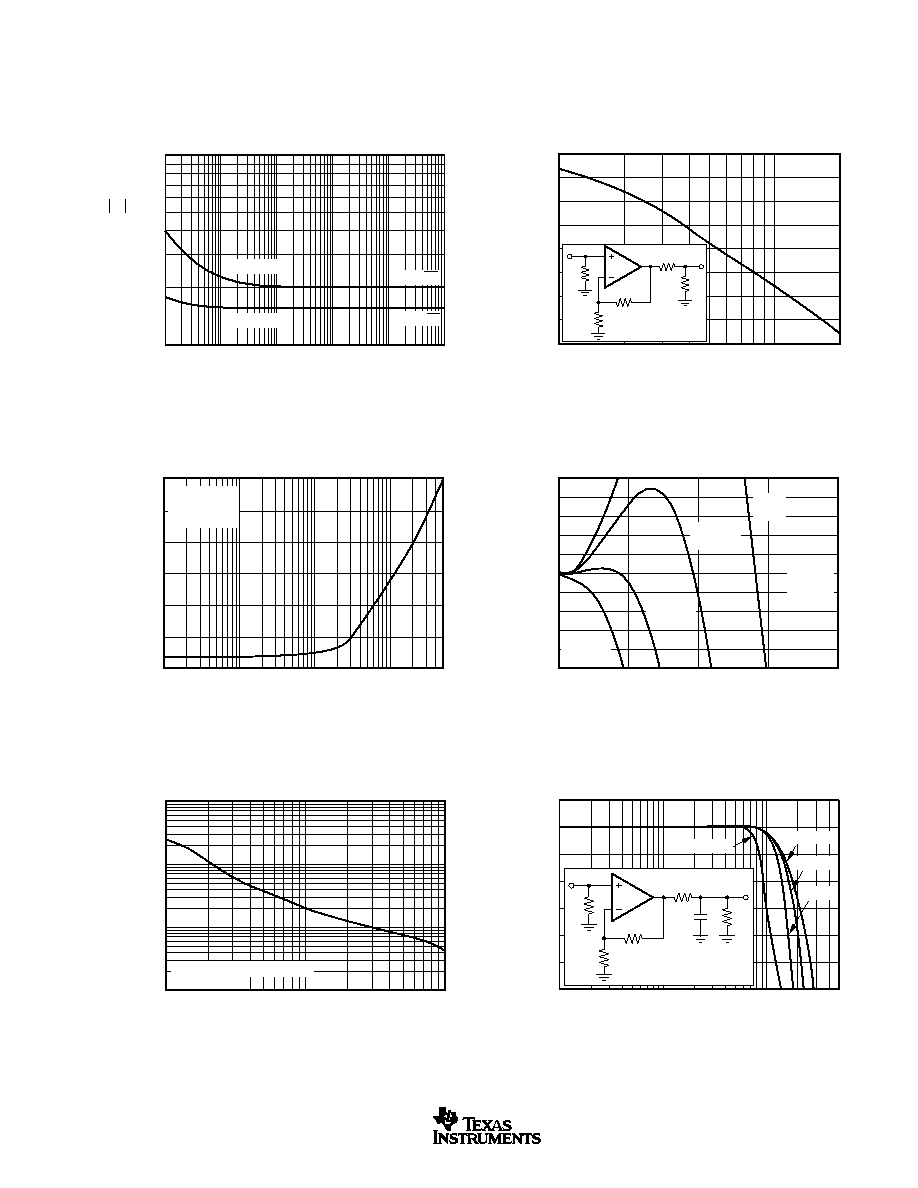
APPLICATIONS INFORMATION
WIDEBAND NONINVERTING OPERATION
The OPA2822 provides a unique combination of features in
a wideband dual, unity-gain stable, voltage-feedback ampli-
fier to support the extremely high dynamic range require-
ments of emerging communications technologies. Combin-
ing low 2nV/
Hz input voltage noise with harmonic distortion
performance that can exceed 100dBc SFDR through 2MHz,
the OPA2822 provides the highest dynamic range input
interface for emerging high speed 14-bit (and higher) con-
verters. To achieve this level of performance, careful atten-
tion to circuit design and board layout is required.
Figure 1 shows the gain of +2 configuration used as the basis
for the Electrical Characteristics table and most of the Typical
Characteristics at
±
6V operation. While the characteristics are
given using split
±
6V supplies, most of the electrical and typical
characteristics also apply to a single-supply +12V design where
the input and output operating voltages are centered at the
midpoint of the +12V supply. Operation at
±
5V will very nearly
match that shown for the
±
6V operating point. Most of the
reference curves were characterized using signal sources with
50
driving impedance, and with measurement equipment
presenting a 50
load impedance. In Figure 1, the 50
shunt
resistor at the V
I
terminal matches the source impedance of the
test signal generator, while the 50
series resistor at the V
O
terminal provides a matching resistor for the measurement
equipment load. Generally, data sheet voltage swing specifica-
tions are at the output pin (V
O
in Figure 1), while output power
(dBm) specifications are at the matched 50
load. The total
100
load at the output, combined with the total 804
total
feedback network load for the noninverting configuration of
Figure 1, presents the OPA2822 with an effective output load of
89
. While this is a good load value for frequency response
measurements, distortion will improve rapidly with lighter output
loads. Keeping the same feedback network and increasing the
load to 200
will result in a total load of 160
for the distortion
performance reported in the Electrical Characteristics table.
For higher gains, the feedback resistor (R
F
) was held at 402
and the gain resistor (R
G
) adjusted to develop the Typical
Characteristics.
Voltage-feedback op amps, unlike current-feedback designs,
can use a wide range of resistor values to set their gains. A low-
noise part like the OPA2822 will deliver low total output noise
only if the resistor values are kept relatively low. For the circuit
of Figure 1, the resistors contribute an input-referred voltage
noise component of 1.8nV/
Hz, which is approaching the value
of the amplifier's intrinsic 2nV/
Hz. For a more complete
description of the feedback network's impact on noise, see the
Setting Resistor Values to Minimize Noise section later in this
data sheet. In general, the parallel combination of R
F
and R
G
should be < 300
to retain the low-noise performance of the
OPA2822. However, setting these values too low can impair
distortion performance due to output loading, as shown in the
distortion versus load data in the Typical Characteristics.
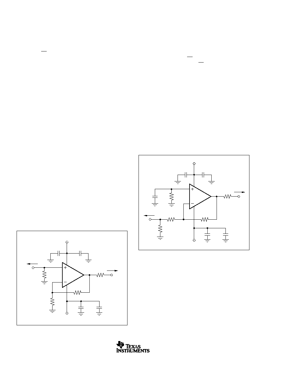
WIDEBAND INVERTING OPERATION
Operating the OPA2822 as an inverting amplifier has several
benefits and is particularly appropriate as part of the hybrid
design in an xDSL receiver application. Figure 2 shows the
inverting gain of 1 circuit used as the basis of the inverting
mode Typical Characteristics.
In the inverting case, only the R
F
element of the feedback
network appears as part of the total output load in parallel
with the actual load. For the 100
load used in the Typical
Characteristics, this gives an effective load of 86
in this
inverting configuration. Gain resistor R
G
is set to achieve the
desired inverting gain (in this case 604
for a gain of 1),
while an additional input matching resistor (R
M
) can be used
to set the total input impedance equal to the source if
desired. In this case, R
M
= 54.9
in parallel with the 604
gain setting resistor yields a matched input impedance of
50
. R
M
is needed only when the input must be matched to
a source impedance, as in the characterization testing done
using the circuit of Figure 2.
FIGURE 1. Noninverting G = +2 Specification and Test
Circuit.
FIGURE 2. Inverting G = 1 Specification and Test
Circuit.
1/2
OPA2822
+5V
5V
V
S
+V
S
50
V
O
V
I
50
+
0.1
µ
F
+
6.8
µ
F
6.8
µ
F
R
G
402
R
F
402
50
Source
50
Load
0.1
µ
F
1/2
OPA2822
+5V
5V
V
S
+V
S
50
V
O
V
I
+
0.1
µ
F
+
6.8
µ
F
6.8
µ
F
R
M
54.9
R
S
309
R
F
604
50
Source
50
Load
0.1
µ
F
0.1
µ
F
R
G
604
OPA2822
15
SBOS188C
www.ti.com
To take full advantage of the OPA2822's excellent DC input
accuracy, the total DC impedance seen at of each of the
input terminals must be matched to get bias current cancel-
lation. For the circuit of Figure 2, this requires the grounded
309
resistor on the noninverting input. The calculation for
this resistor value assumes a DC-coupled 50
source
impedance along with R
G
and R
M
. While this resistor will
provide cancellation for the input bias current, it must be
well decoupled (0.1
µ
F in Figure 2) to filter the noise contri-
bution of the resistor itself and of the amplifier's input
current noise.
As the required R
G
resistor approaches 50
at higher gains,
the bandwidth for the circuit in Figure 2 will far exceed the
bandwidth at the same gain magnitude for the noninverting
circuit of Figure 1. This occurs due to the lower noise gain for
the circuit of Figure 2 when the 50
source impedance is
included in the analysis. For example, at a signal gain of
12 (R
G
= 50
, R
M
= open, R
F
= 604
) the noise gain for the
circuit of Figure 2 will be 1 + 604
/(50
+ 50
) = 7, due to
the addition of the 50
source in the noise gain equation.
This will give considerably higher bandwidth than the nonin-
verting gain of +12.
SINGLE-SUPPLY NONINVERTING OPERATION
The OPA2822 can also support single +5V operation with
its exceptional input and output voltage swing capability.
While not a rail-to-rail input/output design, both inputs and
outputs can swing to within 1.2V of either supply rail. For a
single amplifier channel, this gives a very clean 2V
PP
output
capability on a single +5V supply, or 4V
PP
output for a
differential configuration using both channels together. Fig-
ure 3 shows the AC-coupled noninverting gain of +2 used
as the basis of the Electrical Characteristics table and most
of the Typical Characteristics for single +5V supply opera-
tion.
The key requirement of broadband single-supply operation is
to maintain input and output signal swings within the usable
voltage range at both input and output. The circuit of Figure 3
establishes an input midpoint bias using a simple resistive
divider from the +5V supply (two 804
resistors). These two
resistors are selected to provide DC bias current cancellation
because their parallel combination matches the DC imped-
ance looking out of the inverting node, which equals R
F
. The
gain setting resistor is not part of the DC impedance looking
out of the inverting node, due to the blocking capacitor in
series with it. The input signal is then AC-coupled into the
midpoint voltage bias. The input impedance matching resistor
(57.6
) is selected for testing to give a 50
input match (at
high frequencies) when the parallel combination of the biasing
divider network is included. The gain resistor (R
G
) is AC-
coupled, giving a DC gain of +1. This centers the output also
at the input midpoint bias voltage (V
S
/2). While this circuit is
shown using a +5V supply, this same circuit may be applied
for single-supply operation as high as +12V.
SINGLE-SUPPLY INVERTING OPERATION
For those single +5V Typical Characteristics that require
inverting gain of 1 operation, the test circuit in Figure 4 was
used.
As with the circuit of Figure 2, the feedback resistor (R
F
) has
been increased to 604
to reduce the loading effect it has
in parallel with the 100
actual load. The noninverting input
is biased at V
S
/2 (2.5V in this case) using the two 1.21k
resistors for R
B
. The parallel combination of these two
resistors (605
) provides input bias current cancellation by
matching the DC impedance looking out of the inverting
input node. The noninverting input bias is also well de-
coupled using the 0.1
µ
F capacitor to both reduce both
power-supply noise and the resistor and bias current noise
at this input.
FIGURE 3. AC-Coupled, G = +2, Single-Supply
Operation: Specification and Test Circuit.
FIGURE 4. AC-Coupled, G = 1, Single-Supply
Operation: Specification and Test Circuit.
1/2
OPA2822
+5V
V
S
/2
V
S
/2
+V
S
R
L
100
V
O
V
I
R
B
804
R
B
804
57.6
R
G
402
R
F
402
0.1
µ
F
+
0.1
µ
F
6.8
µ
F
0.1
µ
F
1/2
OPA2822
+5V
V
S
/2
V
S
/2
+V
S
R
L
100
V
O
R
B
1.21k
R
B
1.21k
+
0.1
µ
F
6.8
µ
F
V
I
R
M
54.9
50
Source
R
G
604
R
F
604
0.1
µ
F
0.1
µ
F

OPA2822
16
SBOS188C
www.ti.com
The gain resistor (R
G
) is set to equal the feedback resistor (R
F
)
at 604
to achieve the desired gain of 1 from V
I
to V
O
. A DC
blocking capacitor is included in series with R
G
to reduce the DC
gain for the noninverting input bias and offset voltages to +1.
This places the V
S
/2 bias voltage at the output pin and reduces
the output DC offset error terms. The signal input impedance is
matched to the 50
source using the additional R
M
resistor set
to 54.9
. At higher frequencies, the parallel combination of R
M
and R
G
provides the input impedance match at 50
. This is
principally used for test and characterization purposes--system
applications do not necessarily require this input impedance
match, particularly if the source device is physically near the
OPA2822 and/or does not require a 50
input impedance
match. At higher gains, the signal source impedance will start to
materially impact the apparent noise gain (and hence, band-
width) of the OPA2822.
ADSL RECEIVE AMPLIFIER
One of the principal applications for the OPA2822 is as a low-
power, low-noise receive amplifier in ADSL modem designs.
Applications ranging from single +5V,
±
5V, and up to single +12V
supplies can be well supported by the OPA2822. For higher
supplies, consider the dual, low-noise THS6062 ADSL receive
amplifier that can support up to
±
15V supplies. Figure 5 shows a
typical ADSL receiver design where the OPA2822 is used as an
inverting summing amplifier to provide both driver output signal
cancellation and receive channel gain. In the circuit of Figure 5,
the driver differential output voltage is shown as V
D
, while the
receiver channel output is shown as V
R
.
The two sets of resistors, R
1
and R
2
, are set to provide the
desired gain from the transformer windings for the signal
arriving on the line side of the transformer, and also to provide
nominal cancellation for the driver output signal (V
D
) to the
receiver output. Typically, the two R
S
resistors are set to
provide impedance matching through the transformer. This is
accomplished by setting R
S
= 0.5 · (R
L
/N
2
), where N is the
turns ratio used for the line driver design. If R
S
is set in this
fashion, and the actual twisted pair line shows the expected R
L
impedance value, the voltage swing produced at V
D
will be cut
in half at the transformer input. In this case, setting R
1
= 2 · R
2
will achieve cancellation of the driver output signal at the
output of the receiver. Essentially, the driver output voltage
produces a current in R
1
that is exactly matched by the current
pulled out of R
2
due to the attenuated and inverted version of
the output signal at the transformer input. In actual practice, R
1
and R
2
are usually RC networks to achieve cancellation over
the frequency varying line impedance.
As the transformer turns ratio changes to support different line
driver and supply voltage combinations, the impact of receiver
amplifier noise changes. Typically, DSL systems incur a line
referred noise contribution for the receiver that can be com-
puted for the circuit of Figure 5. For example, targeting an
overall gain of 1 from the line to the receiver output, and
picking the input resistor R
2
, the remaining resistors will be set
by the driver cancellation and gain requirements. With the
resistor values set, a line referred noise contribution due to the
OPA2822 can be computed. R
1
will be set to 2x the value of
R
2
, and the feedback resistor will be set to recover the gain
loss through the transformer. Table I shows the total line
referred noise floor (in dBm/Hz) using three different values for
R
2
over a range of transformer turns ratio (where the amplifier
gain is adjusted at each turns ratio).
Table I shows that a lower transformer turns ratio results in
reduced line referred noise, and that the resistor noise will
start to degrade the noise at higher values--particularly in
going from 500
to 1k
. In general, line referred noise floor
due to the receiver channel will not be the limit to ADSL
modem performance, if it is lower than 145dBm.
FIGURE 5. Example ADSL Receiver Amplifier.
N
R
2
= 200
R
2
= 500
R
2
= 1000
1
151.5
150.2
148.5
1.5
149.1
147.6
145.8
2
147.2
145.6
143.7
2.5
145.6
144.0
142.1
3
144.3
142.7
140.7
3.5
143.2
141.5
139.5
4
142.2
140.5
138.4
4.5
141.3
139.5
137.5
5
140.4
138.7
136.6
TABLE I. Line Referred Noise dBm/Hz, Due to Receiver
Op Amp.
1:n
R
F
R
2
R
S
Driver
1/2
OPA2822
+5V
1/2
OPA2822
5V
R
F
R
2
V
D
R
S
R
1
R
L
V
R
R
1
Line

OPA2822
17
SBOS188C
www.ti.com
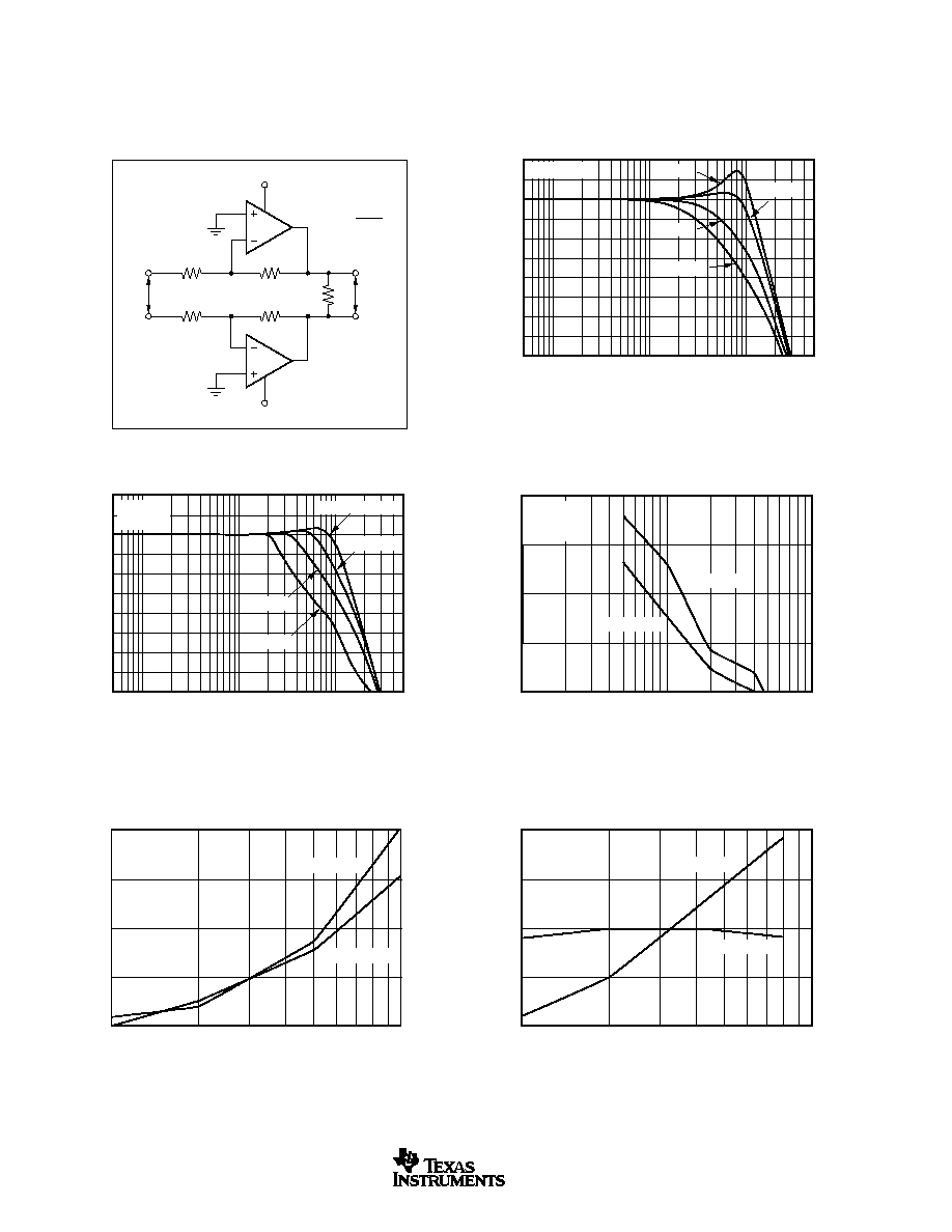
ACTIVE FILTER APPLICATIONS
As a low-noise, low-distortion, unity-gain stable, voltage-
feedback amplifier, the OPA2822 provides an ideal building
block for high-performance active filters. With two channels
available, it can be used either as a cascaded 2-stage active
filter or as a differential filter. Figure 6 shows a 6th-order
bandpass filter cascaded with two 2nd-order Sallen-Key
sections, with transmission zeroes along with a passive post
filter made up of a high-pass and a low-pass section. The first
amplifier provides a 2nd-order high-pass stage while the
second amplifier provides the 2nd-order low-pass stage.
Figure 7 shows the frequency response for this example
filter.
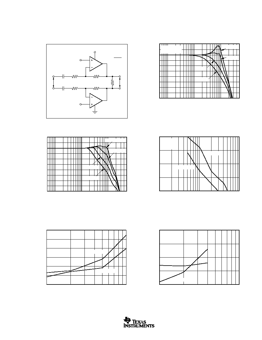
A differential active filter is shown in Figure 8. This circuit
shows a single-supply, 2nd-order high-pass filter with the
corner frequencies set to provide the required high-pass
function for an ADSL CPE modem application. To use this
circuit, the hybrid would be implemented as a passive sum-
ming circuit at the input to this filter. For +5V only ADSL
designs, it is preferable to implement a portion of the filtering
prior to the amplifier, thus limiting the amplitude of the
uncancelled line driver signals. This type of receiver stage
would typically then drive a low-pass filter prior to the codec
setting the high-frequency cutoff of the ADC (Analog-to-
Digital Converter) input signal. Figure 9 shows the frequency
response for the high-pass circuit of Figure 8.
FIGURE 6. 6th-Order Bandpass Filter.
FIGURE 7. Frequency Response for the Filter in Figure 6.
FIGURE 9. Frequency Response for the Filter in Figure 8.
FIGURE 8. Single-Supply, 2nd-Order High-Pass Active
Filter with Differential I/O.
5V
V
O
V
I
1/2
OPA2822
1/2
OPA2822
+5V
225
158
150pF
12pF
18pF
180pF
66pF
150
107
2.1k
140
1.0nF
1.0nF
2.2pF
143
300
1.8nF
1.3k
10
0
10
20
30
40
50
60
Frequency (Hz)
1.0E+04
1.0E+05
1.0E+06
1.0E+08
1.0E+07
Gain (dB)
1/2
OPA2822
+5V
1/2
OPA2822
V
I
V
O
+V
S
V
S
2
2.2
µ
F
2.2
µ
F
2.2
µ
F
2.2
µ
F
365
365
2k
2k
730
730
1
µ
F
3
0
3
6
9
12
15
18
21
24
27
30
Frequency (Hz)
1.0E+04
1.0E+05
1.0E+06
1.0E+07
Gain (dB)

OPA2822
18
SBOS188C
www.ti.com
HIGH DYNAMIC RANGE ADC DRIVER
Numerous circuit approaches exist to provide the last stage
of amplification before the ADC in high-performance applica-
tions. For very high dynamic range applications where the
signal channel can be AC-coupled, the circuit shown in
Figure 10 provides exceptional performance. Most very high
performance ADCs > 12-bit performance require differential
inputs to achieve the dynamic range. The circuit of Figure 10
converts a single-ended source to differential via a 1:2 turns
ratio transformer, which then drives the inverting gain setting
resistors (R
G
). These resistors are fixed at 100
to provide
input matching to a 50
source on the transformer primary
side. The gain can then be adjusted by setting the feedback
resistor values. For best performance, this circuit operates
with a ground centered output on
±
5V supplies, although a
+12V supply can also provide excellent results. Since most
high-performance converters operate on a single +5V sup-
ply, the output is level shifted through an AC blocking
capacitor to the common-mode input voltage (V
CM
) for the
converter input, and then low-pass filtered prior to the input
of the converter. This circuit is intended for inputs from 10kHz
to 10MHz, so the output high-pass corner is set to 1.6kHz,
while the low-pass cutoff is set to 20MHz. These are example
cutoff frequencies; the actual filtering requirements would be
set by the specific application.
The 1:2 turns ratio transformer also provides an improvement
in input referred noise figure. Equation 1 shows the Noise
Figure (NF) calculation for this circuit, where R
G
has been
constrained to provide an input match to R
S
(through the
transformer) and then R
F
is set to get the desired overall
gain. With these constraints (and 0
on the noninverting
inputs), the noise figure equation simplifies considerably.
NF
e
n
i nR
KTR
n
n
S
S
=
+
+
+
+
(
)
10
2
4
2
1
2
1
1
2
2
2
log
/
(1)
where R
G
= 1/2 n
2
R
S
n = Transformer Turns Ratio
= R
F
/R
G
e
n
= Op Amp Input Voltage Noise
i
n
= Inverting Input Current Noise
KT = 4E 21J[T = 290
°
K]
Gain (dB) = 20 log[n
]
REQUIRED
TOTAL GAIN
LOG GAIN
AMPLIFIER GAIN
NOISE FIGURE
(V/V)
(dB)
(
)
(dB)
4
12.0
2
11.2
5
14.0
2.5
10.4
6
15.6
3
9.9
7
16.9
3.5
9.5
8
18.1
4
9.1
9
19.1
4.5
8.9
10
20.0
5
8.6
TABLE II. Noise Figure versus Gain with n = 2 Trans-
former.
FIGURE 10. Single-Ended to Differential High Dynamic Range ADC Driver.
1/2
OPA2822
+5V
1:2
+5V
5V
Noise
Figure
Defined
Here
1/2
OPA2822
V
O
V
I
V
O
V
I
R
F
R
G
V
I
R
F
R
F
R
G
100
R
G
100
V
CM
1k
1k
14-Bit
ADC
0.1
µ
F
80
80
100pF
100pF
1
µ
F
0.1
µ
F
500
V
I
R
S
= 50
= 2

OPA2822
19
SBOS188C
www.ti.com
DESIGN-IN TOOLS
DEMONSTRATION BOARDS
Two PC boards are available to assist in the initial evaluation
of circuit performance using the OPA2822 in its two package
styles. Both of these are available, free, as an unpopulated
PC board delivered with descriptive documentation. The
summary information for these boards is shown in Table I.
Contact your sales representative or go to the TI web site
(www.ti.com) to request these evaluation boards.
Dividing this expression by the noise gain (NG = 1 = R
F
/R
G
)
will give the total equivalent spot noise voltage referred to the
noninverting input, as shown in Equation 3:
E
E
I
R
kTR
I R
NG
kTR
NG
N
NI
BN
S
S
BI
F
F
=
+
(
)
+
+
+
2
2
2
4
4
(3)
Inserting high resistor values into Equation 3 can quickly
dominate the total equivalent input referred voltage noise. A
250
source impedance on the noninverting input will add as
much noise as the amplifier itself. If the noninverting input is
a DC bias path (as in inverting or in some single-supply
applications), it is critical to include a noise shunting capaci-
tor with that resistor to limit the added noise impact of those
resistors (see the example in Figure 2).
FREQUENCY RESPONSE CONTROL
Voltage-feedback op amps such as the OPA2822 exhibit
decreasing closed-loop bandwidth as the signal gain is
increased. In theory, this relationship is described by the
Gain Bandwidth Product (GBP) shown in the Electrical Char-
acteristics. Ideally, dividing GBP by the noninverting signal
gain (also called the Noise Gain, NG) will predict the closed-
loop bandwidth. In practice, this principle holds true only
when the phase margin approaches 90
°
, as it does in higher
gain configurations. At low gains, most high-speed amplifiers
will show a more complex response with lower phase margin
and higher bandwidth than predicted by the GBP. The
OPA2822 is compensated to give a slightly peaked fre-
quency response at a gain of +2 (see the circuit in Figure 1).
The 200MHz typical bandwidth at a gain of +2 far exceeds
that predicted by dividing the GBP of 240MHz by a gain of 2.
The bandwidth predicted by the GBP is more closely correct
as the gain increases. As shown in the Typical Characteris-
tics, at a gain of +10, the 3dB bandwidth of 24MHz matches
that predicted by dividing the GBP by 10.
MACROMODELS AND APPLICATIONS SUPPORT
Computer simulation of circuit performance using SPICE is
often a quick way to analyze the performance of the OPA2822
in its intended application. This is particularly true for video
and RF amplifier circuits where parasitic capacitance and
inductance can play a major role in circuit performance. A
SPICE model for the OPA2822 is available through the TI
web site (www.ti.com). These models do a good job of
predicting small-signal AC and transient performance under
a wide variety of operating conditions. They do not do as well
in predicting the harmonic distortion characteristics. These
models do not attempt to distinguish between the package
types in their small-signal AC performance.
OPERATING SUGGESTIONS
SETTING RESISTOR VALUES TO MINIMIZE NOISE
Getting the full advantage of the OPA2822's low input noise
requires careful attention to the external gain setting and DC
biasing networks. The feedback resistor is part of the overall
output load (which can begin to degrade distortion if set too
low). With this in mind, a good starting point for design is to
select the feedback resistor as low as possible (consistent
with loading distortion concerns), then continue with the
design, and set the other resistors as needed. To retain full
performance, setting the feedback resistor in the range of
200
to 750
can provide a good start to the design.
Figure 11 shows the full output noise analysis model for any
op amp.
The total output spot noise voltage can be computed as the
square root of the sum of all squared output noise voltage
terms. Equation 2 shows the general form of this output noise
voltage expression using the terms shown in Figure 11.
E
E
I
R
kTR NG
I R
kTR
NG
O
NI
BN
S
S
BI
F
F
=
+
(
)
+
(
)
+
(
)
+
2
2
2
2
4
4
(2)
BOARD
LITERATURE
PART
REQUEST
PRODUCT
PACKAGE
NUMBER
NUMBER
OPA2822U
SO-8
DEMOPA268xU
SBOU003
OPA2822E
MSOP-8
DEMOPA26xxE
SBOU004
TABLE I. Demo Board Part Numbers.
FIGURE 11. Op Amp Noise Analysis Model.
4kT
R
G
R
G
R
F
R
S
1/2
OPA2822
I
BI
E
O
I
BN
4kT = 1.6E 20J
at 290
°
K
E
RS
E
NI
4kTR
S
4kTR
F

OPA2822
20
SBOS188C
www.ti.com
Inverting operation offers some interesting opportunities to
increase the available signal bandwidth. When the source
impedance is matched by the gain resistor (Figure 10 for
example), the signal gain is (1 + R
F
/R
G
) while the noise gain
is (1 + R
F
/2R
G
). This reduces the noise gain almost by half,
extending the signal bandwidth and increasing the loop gain.
For instance, setting R
F
= 500
in Figure 10 will give a signal
gain for the amplifier of 5V/V. However, including the 50
source impedance reflected through the 1:2 transformer will
give an additional 100
source impedance for the noise gain
analysis for each of the amplifiers. This reduces the noise gain
to 1 + 500
/200
= 3.5V/V and results in an amplifier
bandwidth of at least 240MHz/3.5 = 68MHz.
DRIVING CAPACITIVE LOADS
One of the most demanding and yet very common load
conditions for an op amp is capacitive loading. Often, the
capacitive load is the input of an ADC, including additional
external capacitance which may be recommended to im-
prove ADC linearity. A high-speed, high open-loop gain
amplifier like the OPA2822 can be very susceptible to de-
creased stability and closed-loop frequency response peak-
ing when a capacitive load is placed directly on the output
pin. When the amplifier's open-loop output resistance is
considered, this capacitive load introduces an additional pole
in the signal path that can decrease the phase margin.
Several external solutions to this problem have been sug-
gested. When the primary considerations are frequency
response flatness with low noise and distortion, the simplest
and most effective solution is to isolate the capacitive load
from the feedback loop by inserting a series isolation resistor
between the amplifier output and the capacitive load. This
does not eliminate the pole from the loop response, but
instead shifts it and adds a zero at a higher frequency. The
additional zero acts to cancel the phase lag from the capaci-
tive load pole, thus increasing the phase margin and improv-
ing stability.
The Typical Characteristics show the recommended R
S
ver-
sus capacitive load and the resulting frequency response at
the load. For the OPA2822 operating at a gain of +2, the
frequency response at the output pin is already slightly
peaked without the capacitive load, requiring relatively high
values of R
S
to flatten the response at the load. One way to
reduce the required R
S
value is to use the noise gain
adjustment circuit of Figure 12.
The resistor across the two inputs, R
NG
, can be used to
increase the noise gain while retaining the desired signal
gain. This can be used either to improve flatness at low gains
or to reduce the required value of R
S
in capacitive load
driving applications. This circuit was used with R
NG
adjusted
to produce the gain flatness curve in the Typical Character-
istics. As shown in that curve, an R
NG
of 452
will give an NG
of 3 giving exceptional frequency response flatness at a
signal gain of +2. Equation 4 shows the calculation for R
NG
given a target noise gain (NG) and signal gain (G):
R
R
R G
NG G
NG
F
S
=
+
-
(4)
where R
S
= Total Source Impedance on the Noninverting
Input [25
in Figure 12]
G = Signal Gain [1 + (R
F
/R
G
)]
NG = Noise Gain Target
Using this technique to get initial frequency response flat-
ness will significantly reduce the required series resistor
value to get a flat response at the capacitive load. Using the
best-case noise gain of 3 with a signal gain of 2 allows the
required R
S
to be reduced, as shown in Figure 13. Here, the
required R
S
versus Capacitive Load is replotted along with
data from the Typical Characteristics. This demonstrates that
the use of R
NG
= 452
across the inputs results in much
lower required R
S
values to achieve a flat response.
FIGURE 12. Noise Gain Tuning for Noninverting Circuit.
1/2
OPA2822
50
R
G
402
R
NG
R
F
402
50
Source
FIGURE 13. Required R
S
vs Noise Gain.
100
10
1
Capacitive Load (pF)
10
100
1000
R
S
(
)
NG = 3, R
NG
= 452
NG = 2, R
NG
=
DISTORTION PERFORMANCE
The OPA2822 is capable of delivering exceptionally low
distortion through approximately 5MHz signal frequency.
While principally intended to provide very low noise and
distortion through the maximum ADSL frequency of 1.1MHz,
the OPA2822 in a differential configuration can deliver lower
than 85dBc distortions for a 4V
PP
swing through 5MHz. For
applications requiring extremely low distortion through higher
frequencies, consider higher slew rate amplifiers such as the
OPA687 or OPA2681.

OPA2822
21
SBOS188C
www.ti.com
As the Typical Characteristics show, until the fundamental
signal reaches very high frequencies or power levels, the
limit to SFDR will be 2nd-harmonic distortion rather than the
negligible 3rd-harmonic component. Focusing then on the
second harmonic, increasing the load impedance improves
distortion directly. However, operating differentially offers
the most significant improvement in even-order distortion
terms. For example, the Electrical Characteristics show that
a single channel of the OPA2822, delivering 2V
PP
at 1MHz
into a 200
load, will typically show a 2nd-harmonic product
at 92dBc versus the 3rd-harmonic at 102dBc. Changing
the configuration to a differential driver where each output
still drives 2V
PP
results in a 4V
PP
total differential output into
a 400
differential load, giving the same single-ended load
of 200
for each amplifier. This configuration drops the
2nd-harmonic to 103dBc and the 3rd-harmonic to approxi-
mately 105dBc--an overall dynamic range improvement
of more than 10dB.
For general distortion analysis, remember that the total
loading on the amplifier includes the feedback network; in the
noninverting configuration, this is the sum of R
F
+ R
G
, while
in the inverting configuration this additional loading is simply
R
F
. Increasing the output voltage swing increases the har-
monic distortion directly. A 6dB increase in the output swing
will generally increase the 2nd-harmonic 12dB and the 3rd-
harmonic 18dB. Increasing the signal gain will also generally
increase both the 2nd- and 3rd-harmonics because the loop
gain decreases at higher gains. Again, a 6dB increase in
voltage gain will increase the 2nd-harmonic distortion by
approximately 6dB. The distortion characteristic curves for
the OPA2822 show little change in the 3rd-harmonic distor-
tion versus gain. Finally, the overall distortion generally
increases as the fundamental frequency increases due to the
rolloff in the loop gain with frequency. Conversely, the distor-
tion will improve going to lower frequencies, down to the
dominant open-loop pole at approximately 50kHz. This will
give essentially unmeasurable levels of harmonic distortion
in the audio band.
The OPA2822 exhibits an extremely low 3rd-order harmonic
distortion. This also gives exceptionally good 2-tone 3rd-
order intermodulation intercept as shown in the Typical
Characteristics. This intercept curve is defined at the 50
load when driven through a 50
matching resistor to allow
direct comparisons to RF MMIC devices. This network at-
tenuates the voltage swing from the output pin to the load by
6dB. If the OPA2822 drives directly into the input of a high-
impedance device, such as an ADC, this 6dB attenuation
does not occur. Under these conditions, the intercept will
improve by at least 6dBm. The intercept is used to predict the
intermodulation spurs for two closely spaced frequencies. If
the two test frequencies, f
1
and f
2
, are specified in terms of
average and delta frequency, f
O
= (f
1
+ f
2
)/2 and
F
= |f
2
f
1
|,
the two, 3rd-order, close-in spurious tones will appear at
f
O
±
3 ·
F
. The difference between two equal test-tone power
levels and the spurious intermodulation power levels is given
by
dBc = 2 · (IM3 P
O
), where IM3 is the intercept taken
from the Typical Specification and P
O
is the power level in
dBm at the 50
load for either one of the two closely spaced
test frequencies. For example, at 1MHz in a gain of +2
configuration, the OPA2822 exhibits an intercept of 57dBm
at a matched 50
load. If the full envelope of the two
frequencies needs to be 2V
PP
, each tone will be set to 4dBm.
The 3rd-order intermodulation spurious tones will then be
2 · (57 4) = 106dBc below the test-tone power level
(102dBm). If this same 2V
PP
2-tone envelope were deliv-
ered directly into the input of an ADC without the matching
loss or loading of the 50
network, the intercept would
increase to at least 63dBm. With the same signal and gain
conditions but now driving directly into a light load, the
spurious tones would then be at least 2 · (63 4) = 118dBc
below the test-tone power levels.
DC ACCURACY AND OFFSET CONTROL
The OPA2822 can provide excellent DC signal accuracy due
to its high open-loop gain, high common-mode rejection, high
power-supply rejection, and low input offset voltage and bias
current offset errors. To take full advantage of the low input
offset voltage (
±
1.2mV maximum at 25
°
C), careful attention
to input bias current cancellation is also required. The high-
speed input stage for the OPA2822 has relatively high input
bias current (8
µ
A typical into the pins) but with a very close
match between the two input currents, typically 100nA input
offset current. The total output offset voltage may be reduced
considerably by matching the source impedances looking out
of the two inputs. For example, one way to add bias current
cancellation to the circuit of Figure 1 would be to insert a
175
series resistor into the noninverting input from the 50
terminating resistor. If the 50
source resistor is DC coupled,
this will increase the source impedance for the noninverting
input bias current to 200
. Since this is now equal to the
impedance looking out of the inverting input (R
F
|| R
G
), the
circuit will cancel the bias current effects, leaving only the
offset current times the feedback resistor as a residual DC
error term at the output. Using a 402
feedback resistor, the
output DC error due to the input bias currents will now be less
than 0.7
µ
A · 402
= 0.28mV over the full temperature range.
This is significantly lower than the contribution due to the
input offset voltage. At a gain of +2, the maximum input offset
voltage is 1.5mV, giving a total maximum output offset of
(
±
3mV
±
0.28mV) =
±
3.3mV over the 40
°
C to +85
°
C
temperature range (for the circuit of Figure 1, including the
additional 175
resistor at the noninverting input).
THERMAL ANALYSIS
The OPA2822 will not require heatsinking or airflow under
most operating conditions. Maximum desired junction tem-
perature will limit the maximum allowed internal power dissi-
pation as described below. In no case should the maximum
junction temperature be allowed to exceed +150
°
C.
Operating junction temperature (T
J
) is given by T
A
+ P
D
JA
.
The total internal power dissipation (P
D
) is the sum of the
quiescent power (P
DO
) and additional power dissipated in the
output stage (P
DL
) to deliver load power. Quiescent power is
simply the specified no-load supply current times the total
supply voltage across the part. P
DL
will depend on the required

OPA2822
22
SBOS188C
www.ti.com
output signal and load but would, for a grounded resistive load,
be at a maximum when the output is fixed at a voltage equal
to half of either supply voltage (assuming equal bipolar sup-
plies). Under this condition P
DL
= V
S
2
/(4 · R
L
) where R
L
includes feedback network loading.
Note that it is the power dissipated in the output stage and not in
the load that determines internal power dissipation. As a worst-
case example, compute the maximum T
J
for the OPA2822E with
both channels operating at A
V
= +2, R
L
= 100
, R
F
= 400
,
±
V
S
=
±
5V, and at the specified maximum T
A
= 85
°
C.
P
D
= 10V · 11.4mA + 2 · (5
2
)/(4 · (100 || 804)) = 255mW
Maximum T
J
= 85
°
C + 0.255W · 150
°
C/W = 123
°
C
This calculation represents a worst-case combination of
conditions to reach a maximum possible operating junction
temperature. Under most operating conditions, the junction
temperature will be far lower than the 123
°
C calculated here.
The output current is limited in the OPA2822 to protect
against damage under short-circuit conditions. This current-
limited output of approximately 220mA exceeds the rated
typical output current of 150mA. The typical and minimum
output current limits are set for linear operation while the
maximum output shown in the Typical Characteristics is
nonlinear limited performance.
BOARD LAYOUT
Achieving optimum performance with a high-frequency am-
plifier like the OPA2822 requires careful attention to board
layout parasitics and external component types. Recommen-
dations that will optimize performance include:
a) Minimize parasitic capacitance to any AC ground for all
of the signal I/O pins. Parasitic capacitance on the output and
inverting input pins can cause instability: on the noninverting
input, it can react with the source impedance to cause
unintentional bandlimiting. To reduce unwanted capacitance,
a window around the signal I/O pins should be opened in all
of the ground and power planes around those pins. Other-
wise, ground and power planes should be unbroken else-
where on the board.
b) Minimize the distance (< 0.25") from the power-supply
pins to high-frequency 0.1
µ
F decoupling capacitors. At the
device pins, the ground and power plane layout should not
be in close proximity to the signal I/O pins. Avoid narrow
power and ground traces to minimize inductance between
the device pins and the decoupling capacitors. The primary
power-supply connections (on pins 4 and 8) should always
be decoupled with these capacitors. Larger (2.2
µ
F to 6.8
µ
F)
decoupling capacitors, effective at lower frequencies, should
also be used on the main supply pins. These may be placed
somewhat farther from the device and may be shared among
several devices in the same area of the PC board.
c) Careful selection and placement of external compo-
nents will preserve the high-frequency performance of
the OPA2822. Resistors should be a very low reactance
type. Surface-mount resistors work best and allow a tighter
overall layout. Metal film and carbon composition axially
leaded resistors can also provide good high-frequency per-
formance. Again, keep their leads and PC board trace length
as short as possible. Never use wire-wound type resistors in
a high-frequency application. Since the output pin and invert-
ing input pin are the most sensitive to parasitic capacitance,
always position the feedback and series output resistor, if
any, as close as possible to the output pin. Other network
components, such as noninverting input termination resis-
tors, should also be placed close to the package. Even with
a low parasitic capacitance shunting the external resistors,
excessively high resistor values can create significant time
constants that can degrade performance. Good axial metal
film or surface-mount resistors have approximately 0.2pF in
shunt with the resistor. For resistor values > 1.5k
, this
parasitic capacitance can add a pole and/or zero below
500MHz that can effect circuit operation. Keep resistor val-
ues as low as possible consistent with parasitic load, distor-
tion, and noise considerations. The 402
feedback used in
the Typical Characteristics is a good starting point for design.
d) Connections to other wideband devices on the board may
be made with short direct traces or through onboard transmission
lines. For short connections, consider the trace and the input to
the next device as a lumped capacitive load. Relatively wide
traces (50mils to 100mils) should be used, preferably with ground
and power planes opened up around them. Estimate the total
capacitive load and set R
S
from the plot of recommended R
S
versus capacitive load. If a long trace is required, and the 6dB
signal loss intrinsic to a doubly-terminated transmission line is
acceptable, implement a matched impedance transmission line
using microstrip or stripline techniques (consult an ECL design
handbook for microstrip and stripline layout techniques). A 50
environment is normally not necessary onboard, and in fact a
higher impedance environment will improve distortion as shown
in the distortion versus load plots. With a characteristic board
trace impedance defined based on board material and trace
dimensions, a matching series resistor into the trace from the
output of the OPA2822 is used as well as a terminating shunt
resistor at the input of the destination device. Remember also that
the terminating impedance will be the parallel combination of the
shunt resistor and the input impedance of the destination device;
this total effective impedance should be set to match the trace
impedance. Multiple destination devices are best handled as
separate transmission lines, each with their own series and shunt
terminations. If the 6dB attenuation of a doubly-terminated trans-
mission line is unacceptable, a long trace can be series-termi-
nated at the source end only. Treat the trace as a capacitive load
in this case and set the series resistor value as shown in the plot
of R
S
vs Capacitive Load. This will not preserve signal integrity as

OPA2822
23
SBOS188C
www.ti.com
well as a doubly-terminated line. If the input impedance of the
destination device is low, there will be some signal attenuation
due to the voltage divider formed by the series output into the
terminating impedance.
e) Socketing a high-speed part like the OPA2822 is not
recommended. The additional lead length and pin-to-pin ca-
pacitance introduced by the socket can create an extremely
troublesome parasitic network, which can make it almost impos-
sible to achieve a smooth, stable frequency response. Best
results are obtained by soldering the OPA2822 onto the board.
INPUT AND ESD PROTECTION
The OPA2822 is built using a very high-speed complementary
bipolar process. The internal junction breakdown voltages are
relatively low due to these very small geometry devices. These
breakdowns are reflected in the Absolute Maximum Rating
table. All device pins are protected with internal ESD protection
diodes to the power supplies, as shown in Figure 14.
These diodes provide moderate protection to input overdrive
voltages above the supplies as well. The protection diodes can
typically support 30mA continuous current. Where higher cur-
rents are possible (e.g. in systems with
±
15V supply parts
driving into the OPA2822), current-limiting series resistors should
be added into the two inputs. Keep these resistor values as low
as possible since high values degrade both noise performance
and frequency response.
FIGURE 14. Internl ESD Protection.
External
Pin
+V
CC
V
CC
Internal
Circuitry

PACKAGING INFORMATION
ORDERABLE DEVICE
STATUS(1)
PACKAGE TYPE
PACKAGE DRAWING
PINS
PACKAGE QTY
OPA2822E/250
ACTIVE
VSSOP
DGK
8
250
OPA2822E/2K5
ACTIVE
VSSOP
DGK
8
2500
OPA2822U
ACTIVE
SOIC
D
8
100
OPA2822U/2K5
ACTIVE
SOIC
D
8
2500
(1) The marketing status values are defined as follows:
ACTIVE: Product device recommended for new designs.
LIFEBUY: TI has announced that the device will be discontinued, and a lifetime-buy period is in effect.
NRND: Not recommended for new designs. Device is in production to support existing customers, but TI does not recommend using this part in
a new design.
PREVIEW: Device has been announced but is not in production. Samples may or may not be available.
OBSOLETE: TI has discontinued the production of the device.
PACKAGE OPTION ADDENDUM
www.ti.com
25-May-2004

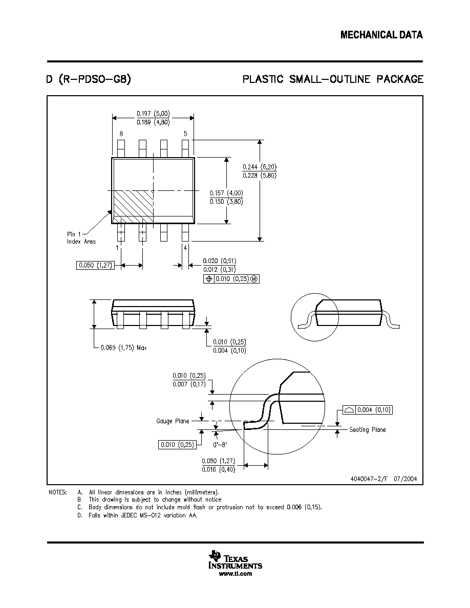

IMPORTANT NOTICE
Texas Instruments Incorporated and its subsidiaries (TI) reserve the right to make corrections, modifications,
enhancements, improvements, and other changes to its products and services at any time and to discontinue
any product or service without notice. Customers should obtain the latest relevant information before placing
orders and should verify that such information is current and complete. All products are sold subject to TI's terms
and conditions of sale supplied at the time of order acknowledgment.
TI warrants performance of its hardware products to the specifications applicable at the time of sale in
accordance with TI's standard warranty. Testing and other quality control techniques are used to the extent TI
deems necessary to support this warranty. Except where mandated by government requirements, testing of all
parameters of each product is not necessarily performed.
TI assumes no liability for applications assistance or customer product design. Customers are responsible for
their products and applications using TI components. To minimize the risks associated with customer products
and applications, customers should provide adequate design and operating safeguards.
TI does not warrant or represent that any license, either express or implied, is granted under any TI patent right,
copyright, mask work right, or other TI intellectual property right relating to any combination, machine, or process
in which TI products or services are used. Information published by TI regarding third-party products or services
does not constitute a license from TI to use such products or services or a warranty or endorsement thereof.
Use of such information may require a license from a third party under the patents or other intellectual property
of the third party, or a license from TI under the patents or other intellectual property of TI.
Reproduction of information in TI data books or data sheets is permissible only if reproduction is without
alteration and is accompanied by all associated warranties, conditions, limitations, and notices. Reproduction
of this information with alteration is an unfair and deceptive business practice. TI is not responsible or liable for
such altered documentation.
Resale of TI products or services with statements different from or beyond the parameters stated by TI for that
product or service voids all express and any implied warranties for the associated TI product or service and
is an unfair and deceptive business practice. TI is not responsible or liable for any such statements.
Following are URLs where you can obtain information on other Texas Instruments products and application
solutions:
Products
Applications
Amplifiers
amplifier.ti.com
Audio
www.ti.com/audio
Data Converters
dataconverter.ti.com
Automotive
www.ti.com/automotive
DSP
dsp.ti.com
Broadband
www.ti.com/broadband
Interface
interface.ti.com
Digital Control
www.ti.com/digitalcontrol
Logic
logic.ti.com
Military
www.ti.com/military
Power Mgmt
power.ti.com
Optical Networking
www.ti.com/opticalnetwork
Microcontrollers
microcontroller.ti.com
Security
www.ti.com/security
Telephony
www.ti.com/telephony
Video & Imaging
www.ti.com/video
Wireless
www.ti.com/wireless
Mailing Address:
Texas Instruments
Post Office Box 655303 Dallas, Texas 75265
Copyright
2004, Texas Instruments Incorporated