8-Bit Transceiver
CY74FCT2245T
SCCS037 - July 1994 - Revised March 2000
Data sheet acquired from Cypress Semiconductor Corporation.
Data sheet modified to remove devices not offered.
Copyright
©
2000, Texas Instruments Incorporated
Features
· Function and pinout compatible with FCT and F logic
· 25
output series resistors to reduce transmission line
reflection noise
· FCT-C speed at 4.1 ns max.
FCT-A speed at 4.6 ns max.
· Edge-rate control circuitry for significantly improved
noise characteristics
· Power-off disable feature
· Fully compatible with TTL input and output logic levels
· ESD > 2000V
· Sink current
12 mA
Source current
15 mA
· Extended commercial temp. range of 40°C to +85°C
· Three-state outputs
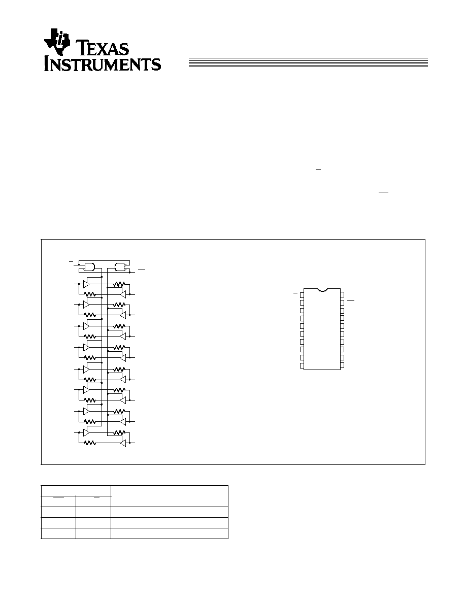
Functional Description
The FCT2245T contains eight non-inverting, bidirectional buffers
with three-state outputs intended for bus oriented applications.
On-chip termination resistors have been added to the outputs to
reduce system noise caused by reflections. For this reason, the
FCT2245T can be used in an existing design to replace the
FCT245T. The FCT2245T current sinking capability is 12 mA at the
A and B ports.
The Transmit/Receive (T/R) input determines the direction of data
flow through the bidirectional transceiver. Transmit (Active HIGH)
enables data from A ports to B ports; receive (Active LOW) enables
data from B ports to A ports. The output enable (OE) input, when
HIGH, disables both the A and B ports by putting them in a High Z
condition.
The outputs are designed with a power-off disable feature to
allow for live insertion of boards.
Function Table
[1]
Inputs
Output
OE
T/R
L
L
Bus B Data to Bus A
L
H
Bus A Data to Bus B
H
X
High Z State
Note:
1.
H = HIGH Voltage Level. L = LOW Voltage Level. X = Don't Care.
Logic Block Diagram
Pin Configurations
FCT2245T1
A
0
A
1
A
2
A
3
A
4
A
5
A
6
A
7
OE
B
0
B
1
B
2
B
3
B
4
B
5
B
6
B
7
T/R
1
2
3
4
5
6
7
8
9
10
11
12
16
17
18
19
20
13
14
V
CC
FCT2245T3
15
Top View
A
0
A
1
A
2
A
3
A
4
A
5
A
6
A
7
OE
B
0
B
1
B
2
B
3
B
4
B
5
B
6
B
7
T/R
GND
DIP/SOIC/QSOP
CY74FCT2245T
2
Maximum Ratings
[2,3]
(Above which the useful life may be impaired. For user guide-
lines, not tested.)
Storage Temperature ................................. 65
°
C to +150
°
C
Ambient Temperature with
Power Applied ............................................. 65
°
C to +135
°
C
Supply Voltage to Ground Potential ............... 0.5V to +7.0V
DC Input Voltage............................................ 0.5V to +7.0V
DC Output Voltage ......................................... 0.5V to +7.0V
DC Output Current (Maximum Sink Current/Pin) ...... 120 mA
Power Dissipation .......................................................... 0.5W
Static Discharge Voltage............................................>2001V
(per MIL-STD-883, Method 3015)
Operating Range
Range
Range
Ambient
Temperature
V
CC
Commercial
T, AT, CT
40
°
C to +85
°
C
5V
±
5%
Electrical Characteristics
Over the Operating Range
Parameter
Description
Test Conditions
Min.
Typ.
[5]
Max.
Unit
V
OH
Output HIGH Voltage
V
CC
=Min., I
OH
=15 mA
Com'l
2.4
3.3
V
V
OL
Output LOW Voltage
V
CC
=Min., I
OL
=12 mA
Com'l
0.3
0.55
V
R
OUT
Output Resistance
V
CC
=Min., I
OL
=12 mA
Com'l
20
25
40
V
IH
Input HIGH Voltage
2.0
V
V
IL
Input LOW Voltage
0.8
V
V
H
Hysteresis
[6]
All inputs
0.2
V
V
IK
Input Clamp Diode Voltage
V
CC
=Min., I
IN
=18 mA
0.7
1.2
V
I
I
Input HIGH Current
V
CC
=Max., V
IN
=V
CC
5
µ
A
I
IH
Input HIGH Current
V
CC
=Max., V
IN
=2.7V
±
1
µ
A
I
IL
Input LOW Current
V
CC
=Max., V
IN
=0.5V
±
1
µ
A
I
OS
Output Short Circuit Current
[7]
V
CC
=Max., V
OUT
=0.0V
60
120
225
mA
I
OFF
Power-Off Disable
V
CC
=0V, V
OUT
=4.5V
±
1
µ
A
Capacitance
[6]
Parameter
Description
Test Conditions
Typ.
[5]
Max.
Unit
C
IN
Input Capacitance
5
10
pF
C
OUT
Output Capacitance
9
12
pF
Notes:
2.
Unless otherwise noted, these limits are over the operating free-air temperature range.
3.
Unused inputs must always be connected to an appropriate logic voltage level, preferably either V
CC
or ground.
4.
T
A
is the "instant on" case temperature.
5.
Typical values are at V
CC
=5.0V, T
A
=+25°C ambient.
6.
This parameter is specified but not tested.
7.
Not more than one output should be shorted at a time. Duration of short should not exceed one second. The use of high-speed test apparatus and/or sample
and hold techniques are preferable in order to minimize internal chip heating and more accurately reflect operational values. Otherwise prolonged shorting of
a high output may raise the chip temperature well above normal and thereby cause invalid readings in other parametric tests. In any sequence of parameter
tests, I
OS
tests should be performed last.
CY74FCT2245T
3
Power Supply Characteristics
Parameter
Description
Test Conditions
Typ.
[5]
Max.
Unit
I
CC
Quiescent Power Supply Current
V
CC
=Max., V
IN
<
0.2V,
V
IN
>
V
CC
0.2V
0.1
0.2
mA
I
CC
Quiescent Power Supply Current
(TTL inputs)
V
CC
=Max., V
IN
=3.4V,
[8]
f
1
=0, Outputs Open
0.5
2.0
mA
I
CCD
Dynamic Power Supply
Current
[9]
V
CC
=Max., One Input Toggling,
50% Duty Cycle, Outputs Open,
T/R=OE=GND,
V
IN
<
0.2V or V
IN
>
V
CC
0.2V
0.06
0.12
mA/MHz
I
C
Total Power Supply Current
[10]
V
CC
=Max., 50% Duty Cycle,
Outputs Open,
One Bit Toggling at f
1
=10 MHz,
T/R=OE=GND,
V
IN
<
0.2V or V
IN
>
V
CC
0.2V
0.7
1.4
mA
V
CC
=Max.,
50% Duty Cycle, Outputs Open,
One Bit Toggling at f
1
=10 MHz,
T/R=OE=GND,
V
IN
=3.4V or V
IN
=GND
1.0
2.4
mA
V
CC
=Max.,
50% Duty Cycle, Outputs Open,
Eight Bits Toggling at f
1
=2.5 MHz,
T/R=OE=GND,
V
IN
<
0.2V or V
IN
>
V
CC
0.2V
1.3
2.6
[11]
mA
V
CC
=Max.,
50% Duty Cycle, Outputs Open,
Eight Bits Toggling at f
1
=2.5 MHz,
T/R=OE=GND,
V
IN
=3.4V or V
IN
=GND
3.3
10.6
[11]
mA
Notes:
8.
Per TTL driven input (V
IN
=3.4V); all other inputs at V
CC
or GND.
9.
This parameter is not directly testable, but is derived for use in Total Power Supply calculations.
10. I
C
= I
QUIESCENT
+ I
INPUTS
+ I
DYNAMIC
I
C
= I
CC
+
I
CC
D
H
N
T
+I
CCD
(f
0
/2 + f
1
N
1
)
I
CC
= Quiescent Current with CMOS input levels
I
CC
= Power Supply Current for a TTL HIGH input (V
IN
=3.4V)
D
H
= Duty Cycle for TTL inputs HIGH
N
T
= Number of TTL inputs at D
H
I
CCD
= Dynamic Current caused by an input transition pair (HLH or LHL)
f
0
= Clock frequency for registered devices, otherwise zero
f
1
= Input signal frequency
N
1
= Number of inputs changing at f
1
All currents are in milliamps and all frequencies are in megahertz.
11. Values for these conditions are examples of the I
CC
formula. These limits are specified but not tested.
CY74FCT2245T
4
]
Switching Characteristics--
Over the Operating Range
[12]
Parameter
Description
FCT2245T
FCT2245AT
FCT2245CT
Unit
Fig.
No.
[13]
Commercial
Commercial
Commercial
Min.
Max.
Min.
Max.
Min.
Max.
t
PLH
t
PHL
Propagation Delay
A
n
to B
n
or B
n
to A
n
1.5
7.0
1.5
4.6
1.5
4.1
ns
1, 3
t
PZH
t
PZL
Output Enable Time
1.5
9.5
1.5
6.2
1.5
5.8
ns
1, 7, 8
t
PHZ
t
PLZ
Output Disable Time
1.5
7.5
1.5
5.0
1.5
4.5
ns
1, 7, 8
Ordering Information--FCT2245T
Speed
(ns)
Ordering Code
Package
Name
Package Type
Operating
Range
4.1
CY74FCT2245CTQCT
Q5
20-Lead (150-Mil) QSOP
Commercial
CY74FCT2245CTSOC/SOCT
S5
20-Lead (300-Mil) Molded SOIC
4.6
CY74FCT2245ATPC
P5
20-Lead (300-Mil) Molded DIP
Commercial
CY74FCT2245ATQCT
Q5
20-Lead (150-Mil) QSOP
CY74FCT2245ATSOC/SOCT
S5
20-Lead (300-Mil) Molded SOIC
7.5
CY74FCT2245TQCT
Q5
20-Lead (150-Mil) QSOP
Commercial
CY74FCT2245TSOC/SOCT
S5
20-Lead (300-Mil) Molded SOIC
Notes:
12. Minimum limits are specified but not tested on Propagation Delays.
13. See "Parameter Measurement Information" in the General Information section.
CY74FCT2245T
5
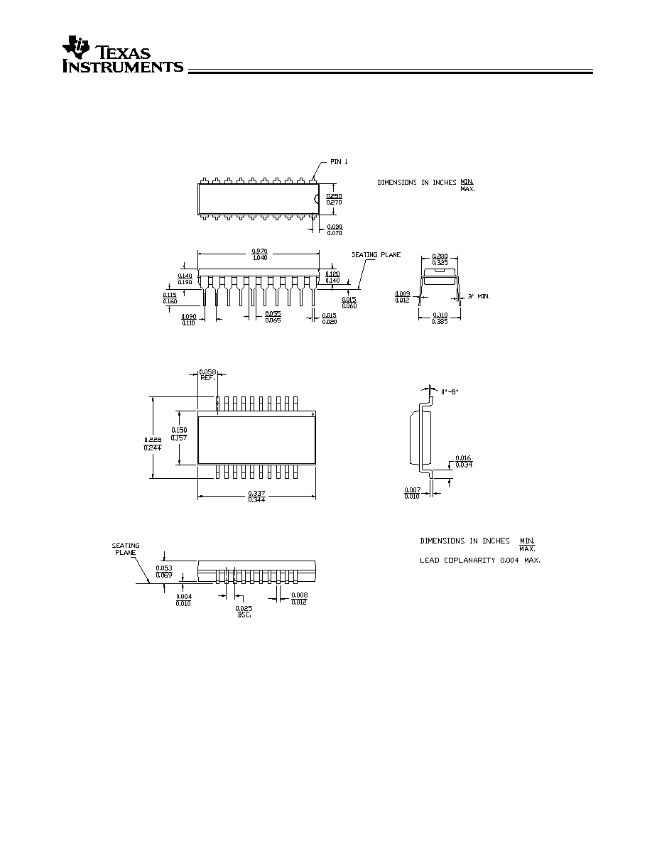
Package Diagrams
20-Lead (300-Mil) Molded DIP P5
20-Lead Quarter Size Outline Q5