
CDCVF25084
3.3-V 1:8 ZERO DELAY (PLL) x4 CLOCK MULTIPLIER
SCAS690A APRIL 2003 REVISED MAY 2003
1
POST OFFICE BOX 655303
·
DALLAS, TEXAS 75265
D
Phase-Locked Loop-Based Multiplier by
Four
D
Input Frequency Range: 2.5 MHz to 45 MHz
D
Output Frequency Range: 10 MHz to
180 MHz
D
LVCMOS/LVTTL I/O Compatible
D
Low Jitter (Cycle-Cycle):
±
120 ps Over the
Range 75 MHz to 180 MHz
D
Distributes One Clock Input to Two Banks
of Four Outputs
D
Auto Frequency Detection to Disable
Device (Power-Down Mode)
D
Operates From Single 3.3-V Supply
D
Industrial Temperature Range 40
°
C to
85
°
C
D
25-
On-Chip Series Damping Resistors
D
No External RC Network Required
D
Spread Spectrum Clock Compatible (SSC)
D
Available in 16-Pin TSSOP Package
description
The CDCVF25084 is a high-performance, low-skew, low-jitter, phase-lock loop clock multiplier. It uses a PLL
to precisely align, in both frequency and phase, the output clocks to the input clock signal including a
multiplication factor of four. The CDCVF25084 operates from a nominal supply voltage of 3.3 V. The device also
includes integrated series-damping resistors in the output drivers that make it ideal for driving point-to-point
loads.
Two banks of four outputs each provide low-skew, low-jitter copies of CLKIN x four. All outputs operate at the
same frequency. Output duty cycles are adjusted to 50%, independent of duty cycle at CLKIN. The device
automatically goes into power-down mode when no input signal is applied to CLKIN and the outputs go into a
low state. Unlike many products containing PLLs, the CDCVF25084 does not require an external RC network.
The loop filter for the PLL is included on-chip, minimizing component count, space, and cost.
Because it is based on a PLL circuitry, the CDCVF25084 requires a stabilization time to achieve phase lock of
the feedback signal to the reference signal. This stabilization is required following power up and application of
a fixed-frequency signal at CLKIN and any following changes to the PLL reference.
The CDCVF25084 is characterized for operation from 40
°
C to 85
°
C.
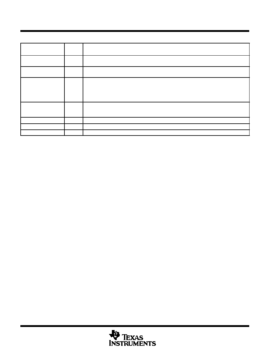
FUNCTION TABLE
S2
S1
1Y01Y3
2Y02Y3
OUTPUT SOURCE
PLL SHUTDOWN
0
0
Hi-Z
Hi-Z
N/A
Yes
0
1
Active
Hi-Z
PLL
No
1
0
Active
Active
Input clock (PLL bypass)
Yes
1
1
Active
Active
PLL
No
A CLK input frequency < 2 MHz switches the outputs to low level.
Copyright
2003, Texas Instruments Incorporated
PRODUCTION DATA information is current as of publication date.
Products conform to specifications per the terms of Texas Instruments
standard warranty. Production processing does not necessarily include
testing of all parameters.
Please be aware that an important notice concerning availability, standard warranty, and use in critical applications of
Texas Instruments semiconductor products and disclaimers thereto appears at the end of this data sheet.
1
2
3
4
5
6
7
8
16
15
14
13
12
11
10
9
CLKIN
1Y0
1Y1
V
DD
GND
2Y0
2Y1
S2
FBIN
1Y3
1Y2
V
DD
GND
2Y3
2Y2
S1
PW PACKAGE (TSSOP)
(TOP VIEW)
CDCVF25084
3.3-V 1:8 ZERO DELAY (PLL) x4 CLOCK MULTIPLIER
SCAS690A APRIL 2003 REVISED MAY 2003
2
POST OFFICE BOX 655303
·
DALLAS, TEXAS 75265
Terminal Functions
TERMINAL
TYPE
DESCRIPTION
NAME
PIN NO.
TYPE
DESCRIPTION
1Y[0:3]
2, 3, 14, 15
O
Bank 1Yn clock outputs. These outputs are low-skew copies of CLKIN. Each output has an integrated
25-
series-damping resistor.
2Y[0:3]
6, 7, 10, 11
O
Bank 2Yn clock outputs. These outputs are low-skew copies of CLKIN. Each output has an integrated
25-
series-damping resistor.
CLKIN
1
I
Clock input. CLKIN provides the clock signal to be distributed by the CDCVF25084 clock driver. CLKIN is
used to provide the reference signal to the integrated PLL that generates the output signal. CLKIN must
have a fixed frequency and phase in order for the PLL to acquire lock. Once the circuit is powered up and
a valid signal is applied, a stabilization time is required for the PLL to phase lock the feedback signal to
CLKIN.
FBIN
16
I
Feedback input. FBIN provides the feedback signal to the internal PLL. FBIN must be wired to one of the
outputs to complete the feedback loop of the internal PLL. The integrated PLL synchronizes the FBIN and
output signal so there is nominally zero-delay from input clock to output clock.
GND
5, 12
Ground
Ground
S1, S2
9, 8
I
Select pins to determine mode of operation. See the FUNCTION TABLE for mode selection options.
VDD
4, 13
Power
Supply voltage. The supply voltage range is 3 V to 3.6 V

CDCVF25084
3.3-V 1:8 ZERO DELAY (PLL) x4 CLOCK MULTIPLIER
SCAS690A APRIL 2003 REVISED MAY 2003
3
POST OFFICE BOX 655303
·
DALLAS, TEXAS 75265
functional block diagram
2
1Y0
PLL
16
FBIN
25
3
1Y1
25
14
1Y2
25
15
1Y3
25
M
U
X
1
CLKIN
Input
Select
Decoding
8
S2
9
S1
6
2Y0
25
7
2Y1
25
10
2Y2
25
11
2Y3
25
Div by 4
CDCVF25084
3.3-V 1:8 ZERO DELAY (PLL) x4 CLOCK MULTIPLIER
SCAS690A APRIL 2003 REVISED MAY 2003
4
POST OFFICE BOX 655303
·
DALLAS, TEXAS 75265
absolute maximum ratings over operating free-air temperature (unless otherwise noted)
Supply voltage range, V
DD
0.5 V to 4.6 V
. . . . . . . . . . . . . . . . . . . . . . . . . . . . . . . . . . . . . . . . . . . . . . . . . . . . . . . . .
Input voltage range, V
I
(see Notes 1 and 2)
0.5 V to 4.6 V
. . . . . . . . . . . . . . . . . . . . . . . . . . . . . . . . . . . . . . . . . .
Output voltage range, V
O
(see Notes 1 and 2)
0.5 V to V
DD
+ 0.5 V
. . . . . . . . . . . . . . . . . . . . . . . . . . . . . . . . . .
Input clamp current, I
IK
(V
I
< 0)
50 mA
. . . . . . . . . . . . . . . . . . . . . . . . . . . . . . . . . . . . . . . . . . . . . . . . . . . . . . . . . . .
Output clamp current, I
OK
(V
O
< 0)
50 mA
. . . . . . . . . . . . . . . . . . . . . . . . . . . . . . . . . . . . . . . . . . . . . . . . . . . . . . . .
Continuous total output current, I
O
(V
O
= 0 to V
DD
)
±
50 mA
. . . . . . . . . . . . . . . . . . . . . . . . . . . . . . . . . . . . . . . . . .
Package thermal impedance,
JA
(see Note 3): PW package
147
°
C/W
. . . . . . . . . . . . . . . . . . . . . . . . . . . . . . .
Storage temperature range, T
stg
65
°
C to 150
°
C
. . . . . . . . . . . . . . . . . . . . . . . . . . . . . . . . . . . . . . . . . . . . . . . . . . .
Stresses beyond those listed under "absolute maximum ratings" may cause permanent damage to the device. These are stress ratings only, and
functional operation of the device at these or any other conditions beyond those indicated under "recommended operating conditions" is not
implied. Exposure to absolute-maximum-rated conditions for extended periods may affect device reliability.
NOTES:
1. The input and output negative voltage ratings may be exceeded if the input and output clamp-current ratings are observed.
2. This value is limited to 4.6 V maximum.
3. The package thermal impedance is calculated in accordance with JESD 51.
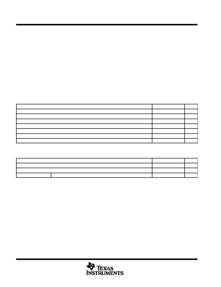
recommended operating conditions
MIN
NOM
MAX
UNIT
Supply voltage, VDD
3
3.3
3.6
V
Low level input voltage, VIL
0.8
V
High level input voltage, VIH
2
V
Input voltage, VI
0
3.6
V
High-level output current, IOH
12
mA
Low-level output current, IOL
12
mA
Operating free-air temperature, TA
40
85
°
C
timing requirements over recommended ranges of supply voltage, load and operating free-air
temperature
MIN
NOM
MAX
UNIT
Input clock frequency, fCLKIN
2.5
45
MHz
Input clock duty cycle
40%
60%
Clock frequency, fclkout
CL = 15 pF
10
180
MHz

CDCVF25084
3.3-V 1:8 ZERO DELAY (PLL) x4 CLOCK MULTIPLIER
SCAS690A APRIL 2003 REVISED MAY 2003
5
POST OFFICE BOX 655303
·
DALLAS, TEXAS 75265
electrical characteristics over recommended operating free-air temperature range (unless
otherwise noted)
PARAMETER
TEST CONDITIONS
MIN
TYP
MAX
UNIT
VIK
Input voltage
VDD = 3 V,
II = 18 mA
1.2
V
II
Input current
VI = 0 V or VDD
±
5
µ
A
IPD
Power-down current
fCLKIN = 0 MHz,
VDD = 3.3 V
100
µ
A
IDD
Dynamic current
fout = 80 MHz,
CL = 15 pF
60
80
mA
IOZ
Output 3-state
Vo = 0 V or VDD,
VDD = 3.6 V
±
5
µ
A
CI
Input capacitance at FBIN, CLKIN
VI = 0 V or VDD
4
pF
CI
Input capacitance at S1, S2
VI = 0 V or VDD
2.2
pF
CO
Output capacitance
VI = 0 V or VDD
3
pF
VDD = min to max,
IOH = 100
µ
A
VDD 0.2
VOH
High-level output voltage
VDD = 3 V,
IOH = 12 mA
2.1
V
VOH
High level out ut voltage
VDD = 3 V,
IOH = 6 mA
2.4
V
VDD = min to max,
IOL = 100
µ
A
0.2
VOL
Low-level output voltage
VDD = 3 V,
IOL = 12 mA
0.8
V
VOL
Low level out ut voltage
VDD = 3 V,
IOL = 6 mA
0.55
V
VDD = 3 V,
VO = 1 V
24
IOH
High-level output current
VDD = 3.3 V,
VO = 1.65 V
30
mA
IOH
High level out ut current
VDD = 3.6 V,
VO = 3.135 V
-15
mA
VDD = 3 V,
VO = 1.95 V
26
IOL
Low-level output current
VDD = 3.3 V,
VO = 1.65 V
33
mA
OL
VDD = 3.6 V,
VO = 0.4 V
14
All typical values are at respective nominal VDD.
All outputs are switching; for IDD over frequency see Figure 9.