CDC329
1-LINE TO 6-LINE CLOCK DRIVER
WITH SELECTABLE POLARITY
SCBS117AD4501, JANUARY 1991REVISED NOVEMBER 1992
Copyright
©
1992, Texas Instruments Incorporated
1
POST OFFICE BOX 655303
·
DALLAS, TEXAS 75265
·
Low Output Skew for Clock-Distribution
and Clock-Generation Applications
·
State-of-the-Art
EPIC-
B
TM
BiCMOS Design
Significantly Reduces Power Dissipation
·
TTL-Compatible Inputs and
CMOS-Compatible Outputs
·
Distributes One Clock Input to Six Clock
Outputs
·
Polarity Control Selects True or
Complementary Outputs
·
Distributed V
CC
and GND Pins Reduce
Switching Noise
·
High-Drive Outputs (15-mA I
OH
,
64-mA I
OL
)
·
Packaged in Plastic Small-Outline Package
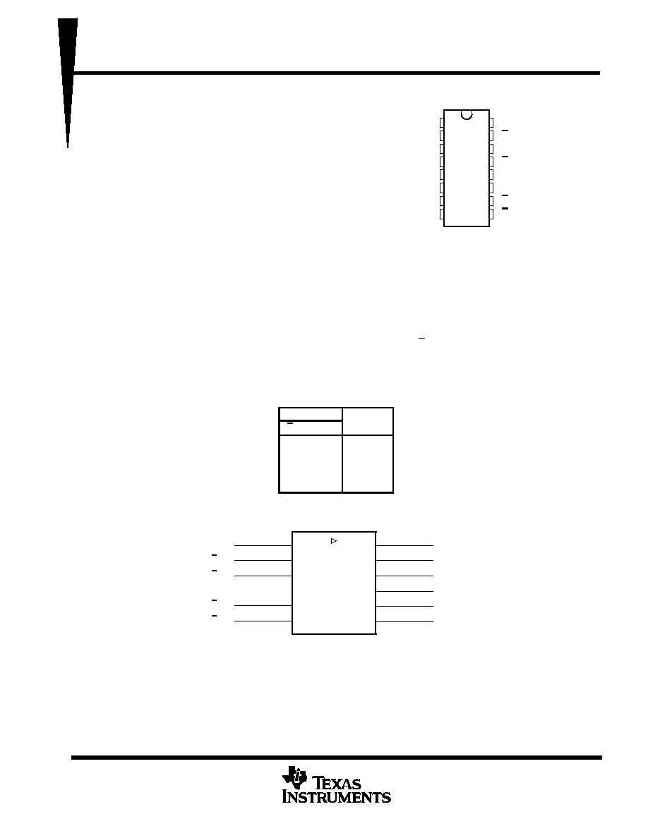
description
The CDC329 contains a clock driver circuit that distributes one input signal to six outputs with minimum skew
for clock distribution. Through the use of the polarity control inputs (T/C), various combinations of true and
complementary outputs can be obtained.
The CDC329 is characterized for operation from 40
°
C to 85
°
C.
FUNCTION TABLE
INPUTS
OUTPUT
T/C
A
Y
L
L
L
L
H
H
H
L
H
H
H
L
logic symbol
12
A
N1
15
N2
13
1Y1
16
1
1Y2
2
1
2Y1
3
2
N3
10
N4
9
2Y2
5
2
3Y
6
3
4Y
8
4
1T/C
2T/C
3T/C
4T/C
This symbol is in accordance with ANSI/IEEE Std 91-1984 and IEC Publication 617-12.
D PACKAGE
(TOP VIEW)
1
2
3
4
5
6
7
8
16
15
14
13
12
11
10
9
GND
1Y2
2Y1
GND
2Y2
3Y
GND
4Y
1Y1
1T/C
V
CC
2T/C
A
V
CC
3T/C
4T/C
EPIC-
B is a trademark of Texas Instruments Incorporated.
PRODUCTION DATA information is current as of publication date.
Products conform to specifications per the terms of Texas Instruments
standard warranty. Production processing does not necessarily include
testing of all parameters.

CDC329
1-LINE TO 6-LINE CLOCK DRIVER
WITH SELECTABLE POLARITY
SCBS117AD4501, JANUARY 1991REVISED NOVEMBER 1992
2
POST OFFICE BOX 655303
·
DALLAS, TEXAS 75265
logic diagram (positive logic)
1Y1
1Y2
2Y1
2Y2
3Y
4Y
16
2
3
5
6
8
15
13
12
10
9
1T/C
A
2T/C
3T/C
4T/C
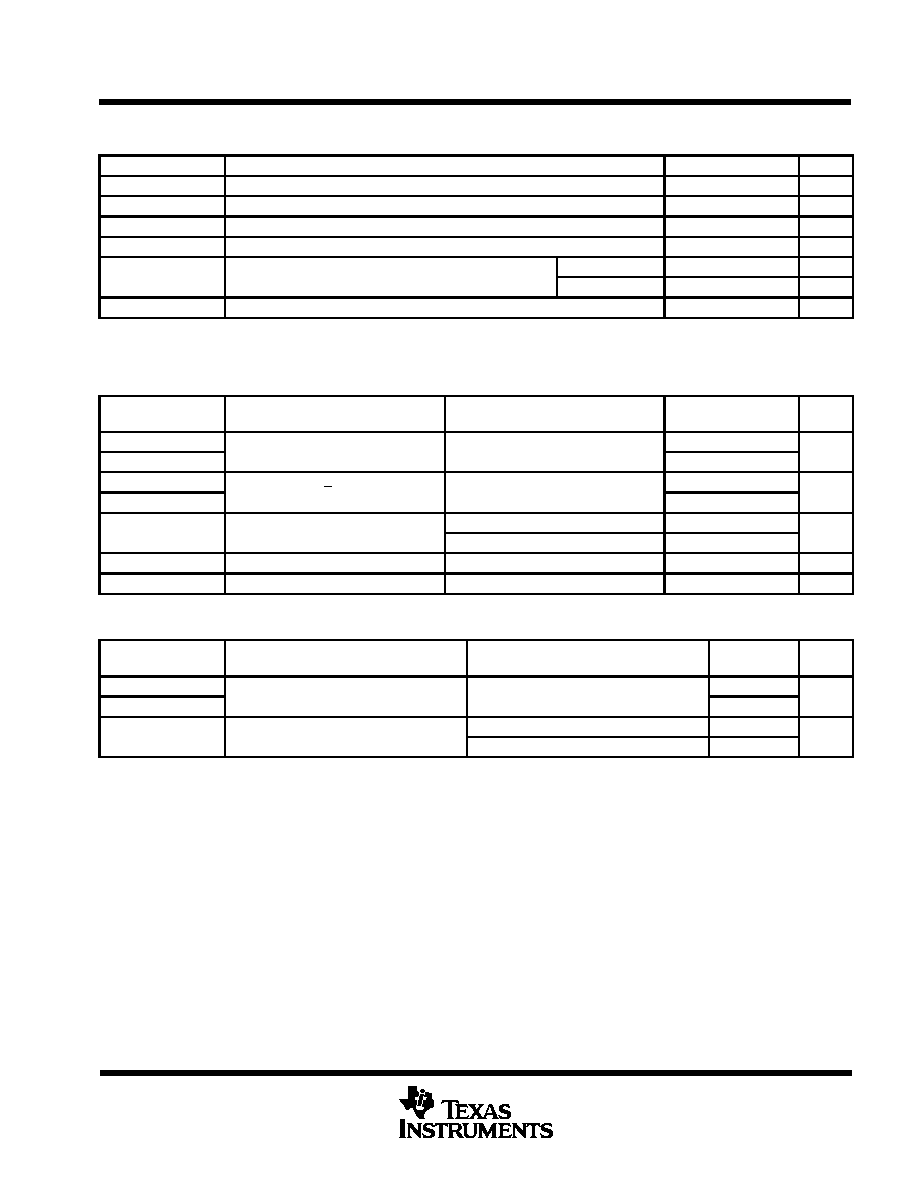
absolute maximum ratings over operating free-air temperature range (unless otherwise noted)
Supply voltage range, V
CC
0.5 V to 7 V
. . . . . . . . . . . . . . . . . . . . . . . . . . . . . . . . . . . . . . . . . . . . . . . . . . . . . . . . . .
Input voltage range, V
I
(see Note 1)
1.2 V to 7 V
. . . . . . . . . . . . . . . . . . . . . . . . . . . . . . . . . . . . . . . . . . . . . . . . . .
Voltage range applied to any output in the high state
or power-off state, V
O
(see Note 1)
0.5 V to V
CC
+ 0.5 V
. . . . . . . . . . . . . . . . . . . . . . . . . . . . . . . . . . . . .
Current into any output in the low state, I
O
128 mA
. . . . . . . . . . . . . . . . . . . . . . . . . . . . . . . . . . . . . . . . . . . . . . . . .
Input clamp current, I
IK
(V
I
< 0)
18 mA
. . . . . . . . . . . . . . . . . . . . . . . . . . . . . . . . . . . . . . . . . . . . . . . . . . . . . . . . . . .
Output clamp current, I
OK
(V
O
< 0)
50 mA
. . . . . . . . . . . . . . . . . . . . . . . . . . . . . . . . . . . . . . . . . . . . . . . . . . . . . . .
Continuous total power dissipation at (or below) 25
°
C free-air temperature (see Note 2)
1000 mW
. . . . . . . .
Storage temperature range
65
°
C to 150
°
C
. . . . . . . . . . . . . . . . . . . . . . . . . . . . . . . . . . . . . . . . . . . . . . . . . . . . . . .
Stresses beyond those listed under "absolute maximum ratings" may cause permanent damage to the device. These are stress ratings only, and
functional operation of the device at these or any other conditions beyond those indicated under "recommended operating conditions" is not
implied. Exposure to absolute-maximum-rated conditions for extended periods may affect device reliability.
NOTES:
1. The input and output negative-voltage ratings may be exceeded if the input and output clamp-current ratings are observed.
2. For operation above 25
°
C free-air temperature, derate to 478 mW at 85
°
C at the rate of 8.7 mW/
°
C.
recommended operating conditions (see Note 3)
MIN
NOM
MAX
UNIT
VCC
Supply voltage
4.75
5
5.25
V
VIH
High-level input voltage
2
V
VIL
Low-level input voltage
0.8
V
VI
Input voltage
0
VCC
V
IOH
High-level output current
15
mA
IOL
Low-level output current
64
mA
t /
v
Input transition rise or fall rate
5
ns / V
TA
Operating free-air temperature
40
85
°
C
NOTE 3: Unused inputs must be held high or low.
CDC329
1-LINE TO 6-LINE CLOCK DRIVER
WITH SELECTABLE POLARITY
SCBS117AD4501, JANUARY 1991REVISED NOVEMBER 1992
3
POST OFFICE BOX 655303
·
DALLAS, TEXAS 75265
electrical characteristics over recommended operating free-air temperature range (unless
otherwise noted)
PARAMETER
TEST CONDITIONS
MIN
TYP
MAX
UNIT
VIK
VCC = 4.75 V,
II = 18 mA
1.2
V
VOH
VCC = 4.75 V,
IOH = 15 mA
3.85
V
VOL
VCC = 4.75 V,
IOL = 64 mA
0.55
V
II
VCC = 5.25 V,
VI = VCC or GND
±
1
µ
A
ICC
VCC = 5.25 V,
IO = 0,
Outputs high
50
µ
A
ICC
CC
,
O
,
VI = VCC or GND
Outputs low
20
30
mA
Ci
VI = 2.5 V or 0.5 V
3
pF
All typical values are at VCC = 5 V, TA = 25
°
C
switching characteristics over recommended ranges of supply voltage and operating free-air
temperature (see Figures 1 and 2)
PARAMETER
FROM
(INPUT)
TO
(OUTPUT)
MIN
TYP
MAX
UNIT
tPLH
A
Any Y
2
6.6
ns
tPHL
A
Any Y
1.7
5.4
ns
tPLH
T/C
Any Y
1.6
7.4
ns
tPHL
T/C
Any Y
1.7
6.3
ns
t k( )
A
Any Y (same phase)
0.5
ns
tsk(o)
A
Any Y (any phase)
2.5
ns
tr
2
ns
tf
1.3
ns
switching characteristics, V
CC
= 5 V
±
0.25 V, T
A
= 25
°
C to 70
°
C (see Figures 1 and 2)
PARAMETER
FROM
(INPUT)
TO
(OUTPUT)
MIN
MAX
UNIT
tPLH
A
Any Y
2.3
5.9
ns
tPHL
A
Any Y
1.7
4.8
ns
t k( )
A
Any Y (same phase)
0.5
ns
tsk(o)
A
Any Y (any phase)
2
ns

CDC329
1-LINE TO 6-LINE CLOCK DRIVER
WITH SELECTABLE POLARITY
SCBS117AD4501, JANUARY 1991REVISED NOVEMBER 1992
4
POST OFFICE BOX 655303
·
DALLAS, TEXAS 75265
PARAMETER MEASUREMENT INFORMATION
From Output
Under Test
CL = 50 pF
(see Note A)
LOAD CIRCUIT FOR OUTPUTS
500
tPLH
tPHL
1.5 V
1.5 V
3 V
0 V
50% VCC
50% VCC
VOH
VOL
80% VCC
20% VCC
20% VCC
tf
tr
Input
(see Note B)
VOLTAGE WAVEFORMS
PROPAGATION DELAY TIMES
Output
NOTES: A. CL includes probe and jig capacitance.
B. All input pulses are supplied by generators having the following characteristics: PRR
10 MHz, ZO = 50
, tr
2.5 ns, tf
2.5 ns.
Figure 1. Load Circuit and Voltage Waveforms

CDC329
1-LINE TO 6-LINE CLOCK DRIVER
WITH SELECTABLE POLARITY
SCBS117AD4501, JANUARY 1991REVISED NOVEMBER 1992
5
POST OFFICE BOX 655303
·
DALLAS, TEXAS 75265
WAVEFORMS FOR CALCULATION OF t
sk(o)
tPLH1
2Y2
2Y1
2T/C
1Y2
1Y1
1T/C
A
tPHL1
tPLH5
tPHL5
tPLH2
tPHL2
tPLH6
tPHL6
tPLH3
tPHL3
tPHL7
tPLH7
tPLH4
tPHL4
tPHL8
tPLH8
Output skew, tsk(o), from A to any Y (same phase), can be measured only between outputs for which the respective polarity control inputs (T/C)
are at the same logic level. It is calculated as the greater of:
a) the difference between the fastest and slowest of tPLH from A
to any Y
(e.g.,
tPLHn, n = 1 to 4; or tPLHn, n = 5 to 6),
b) the difference between the fastest and slowest of tPHL from A
to any Y
(e.g., tPHLn, n = 1 to 4; or tPHLn, n = 5 to 6),
c) the difference between the fastest and slowest of tPLH from A
to any Y
(e.g., tPLHn, n = 7 to 8), and
d) the difference between the fastest and slowest of tPHL from A
to any Y
(e.g., tPHLn, n = 7 to 8).
Output skew, tsk(o), from A to any Y (any phase), can be measured between outputs for which the respective polarity control inputs (T/C) are at
the same or different logic levels. It is calculated as the greater of:
a) the difference between the fastest and slowest of tPLH from A
to any Y or tPHL from A
to any Y
(e.g., tPLHn, n = 1 to 4; or tPLHn, n = 5 to 6, and tPHLn, n = 7 to 8), and
b) the difference between the fastest and slowest of tPHL from A
to any Y or tPLH from A
to any Y
(e.g., tPHLn, n = 1 to 4; or tPHLn, n = 5 to 6, and tPLHn, n = 7 to 8).
Figure 2. Skew Waveforms and Calculations