1
Data sheet acquired from Harris Semiconductor
SCHS165
Features
· Asynchronous Master Reset
· J, K, (D) Inputs to First Stage
· Fully Synchronous Serial or Parallel Data Transfer
· Shift Right and Parallel Load Capability
· Complementary Output From Last Stage
· Buffered Inputs
· Typical f
MAX
= 50MHz at V
CC
= 5V,
C
L
= 15pF, T
A
= 25
o
C
· Fanout (Over Temperature Range)
- Standard Outputs . . . . . . . . . . . . . . . 10 LSTTL Loads
- Bus Driver Outputs . . . . . . . . . . . . . 15 LSTTL Loads
· Wide Operating Temperature Range . . . -55
o
C to 125
o
C
· Balanced Propagation Delay and Transition Times
· Significant Power Reduction Compared to LSTTL
Logic ICs
· HC Types
- 2V to 6V Operation
- High Noise Immunity: N
IL
= 30%, N
IH
= 30%of V
CC
at
V
CC
= 5V
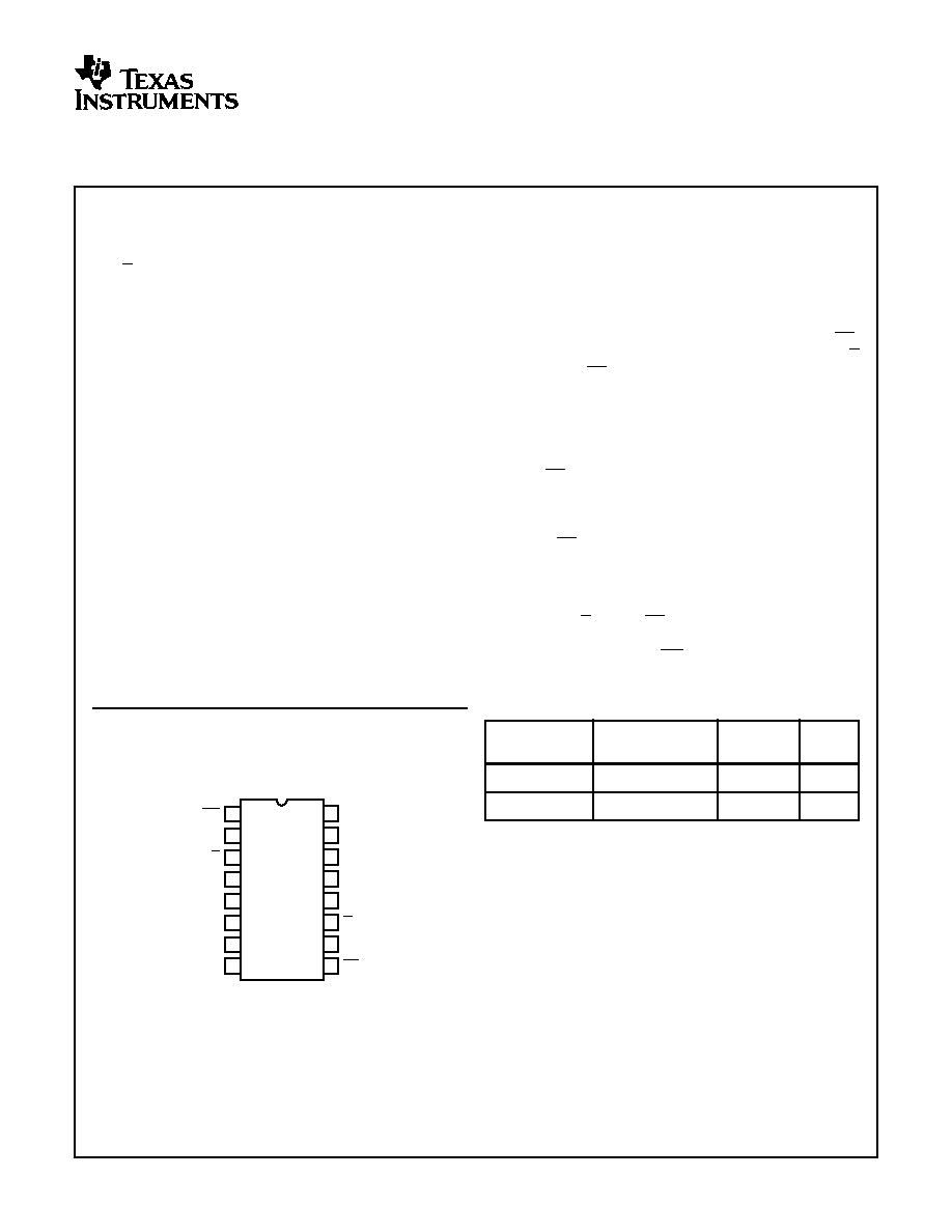
PInout
CD74HC195
(PDIP, SOIC)
TOP VIEW
Description
The device is useful in a wide variety of shifting, counting
and storage applications. It performs serial, parallel, serial to
parallel, or parallel to serial data transfers at very high
speeds.
The two modes of operation, shift right (Q
0
-Q
1
) and parallel
load, are controlled by the state of the Parallel Enable (PE)
input. Serial data enters the first flip-flop (Q
0
) via the J and K
inputs when the PE input is high, and is shifted one bit in the
direction Q
0
-Q
1
-Q
2
-Q
3
following each Low to High clock
transition. The J and K inputs provide the flexibility of the JK-
type input for special applications and by tying the two pins
together, the simple D-type input for general applications.
The device appears as four common-clocked D flip-flops
when the PE input is Low. After the Low to High clock transi-
tion, data on the parallel inputs (D0-D3) is transferred to the
respective Q
0
-Q
3
outputs. Shift left operation (Q
3
-Q
2
) can
be achieved by tying the Q
n
outputs to the Dn-1 inputs and
holding the PE input low.
All parallel and serial data transfers are synchronous, occurring
after each Low to High clock transition. The CD74HC195 series
utilizes edge triggering; therefore, there is no restriction on the
activity of the J, K, Pn and PE inputs for logic operations, other
than set-up and hold time requirements. A Low on the
asynchronous Master Reset (MR) input sets all Q outputs Low,
independent of any other input condition.
14
15
16
9
13
12
11
10
1
2
3
4
5
7
6
8
MR
J
K
D0
D1
D2
GND
D3
V
CC
Q
1
Q
2
Q
3
Q
3
CP
PE
Q
0
Ordering Information
PART NUMBER
TEMP. RANGE (
o
C)
PACKAGE
PKG.
NO.
CD74HC195E
-55 to 125
16 Ld PDIP
E16.3
CD74HC195M
-55 to 125
16 Ld SOIC
M16.15
NOTES:
1. When ordering, use the entire part number.
2. Die for this part number is available which meets all electrical
specifications. Please contact your local sales office or Harris
customer service for ordering information.
September 1997
CAUTION: These devices are sensitive to electrostatic discharge. Users should follow proper IC Handling Procedures.
Copyright
©
Harris Corporation 1997
File Number
1482.1
CD74HC195
High Speed CMOS Logic
4-Bit Parallel Access Register
[ /Title
(CD74
HC195
)
/Sub-
ject
(High
Speed
CMOS
Logic
4-Bit
Paral-
lel
Access
Regis-
ter)
/Autho

2
Functional Diagram
TRUTH TABLE
OPERATING MODES
INPUTS
OUTPUT
MR
CP
PE
J
K
Dn
Q
0
Q
1
Q
2
Q
3
Q
3
Asynchronous Reset
L
X
X
X
X
X
L
L
L
L
H
Shift, Set First Stage
H
h
h
h
X
H
q
0
q
1
q
2
q
2
Shift, Reset First Stage
H
h
l
l
X
L
q
0
q
1
q
2
q
2
Shift, Toggle First Stage
H
h
h
l
X
q
0
q
0
q
1
q
2
q
2
Shift, Retain First Stage
H
h
l
h
X
q
0
q
0
q
1
q
2
q
2
Parallel Load
H
l
X
X
dn
d
0
d
1
d
2
d3
d2
NOTE: H = High Voltage Level
L = Low Voltage Level,
X = Don't Care
= Transition from Low to High Level
l = Low Voltage Level One Set-up Time Prior to the Low to High Clock Transition
h = Low Voltage Level One Set-up Time prior to the High to Low Clock Transition,
dn (q
n
) = Lower Case Letters Indicate the State of the Referenced Input (or output) One Set-up Time Prior to the Low to High Clock
Transition.
11
Q
3
1
2
10
3
J
CP
K
MR
15
14
13
12
9
4
5
6
7
Q
0
Q
1
Q
2
Q
3
D
0
D
1
D
2
D
3
PE
CD74HC195

3
Absolute Maximum Ratings
Thermal Information
DC Supply Voltage, V
CC
. . . . . . . . . . . . . . . . . . . . . . . . -0.5V to 7V
DC Input Diode Current, I
IK
For V
I
< -0.5V or V
I
> V
CC
+ 0.5V
. . . . . . . . . . . . . . . . . . . . . .±
20mA
DC Output Diode Current, I
OK
For V
O
< -0.5V or V
O
> V
CC
+ 0.5V
. . . . . . . . . . . . . . . . . . . .±
20mA
DC Output Source or Sink Current per Output Pin, I
O
For V
O
> -0.5V or V
O
< V
CC
+ 0.5V
. . . . . . . . . . . . . . . . . . . .±
25mA
DC V
CC
or Ground Current, I
CC or
I
GND
. . . . . . . . . . . . . . . . . .±
50mA
Operating Conditions
Temperature Range (T
A
) . . . . . . . . . . . . . . . . . . . . . -55
o
C to 125
o
C
Supply Voltage Range, V
CC
HC Types . . . . . . . . . . . . . . . . . . . . . . . . . . . . . . . . . . . . .2V to 6V
HCT Types . . . . . . . . . . . . . . . . . . . . . . . . . . . . . . . . .4.5V to 5.5V
DC Input or Output Voltage, V
I
, V
O
. . . . . . . . . . . . . . . . . 0V to V
CC
Input Rise and Fall Time
2V . . . . . . . . . . . . . . . . . . . . . . . . . . . . . . . . . . . . . . 1000ns (Max)
4.5V. . . . . . . . . . . . . . . . . . . . . . . . . . . . . . . . . . . . . . 500ns (Max)
6V . . . . . . . . . . . . . . . . . . . . . . . . . . . . . . . . . . . . . . . 400ns (Max)
Thermal Resistance (Typical, Note 3)
JA
(
o
C/W)
PDIP Package . . . . . . . . . . . . . . . . . . . . . . . . . . . . .
90
SOIC Package . . . . . . . . . . . . . . . . . . . . . . . . . . . . .
190
Maximum Junction Temperature . . . . . . . . . . . . . . . . . . . . . . . 150
o
C
Maximum Storage Temperature Range . . . . . . . . . .-65
o
C to 150
o
C
Maximum Lead Temperature (Soldering 10s) . . . . . . . . . . . . . 300
o
C
(SOIC - Lead Tips Only)
CAUTION: Stresses above those listed in "Absolute Maximum Ratings" may cause permanent damage to the device. This is a stress only rating and operation
of the device at these or any other conditions above those indicated in the operational sections of this specification is not implied.
NOTE:
3.
JA
is measured with the component mounted on an evaluation PC board in free air.
DC Electrical Specifications
PARAMETER
SYMBOL
TEST
CONDITIONS
V
CC
(V)
25
o
C
-40
o
C TO 85
o
C -55
o
C TO 125
o
C
UNITS
V
I
(V)
I
O
(mA)
MIN
TYP
MAX
MIN
MAX
MIN
MAX
High Level Input
Voltage
V
IH
-
-
2
1.5
-
-
1.5
-
1.5
-
V
4.5
3.15
-
-
3.15
-
3.15
-
V
6
4.2
-
-
4.2
-
4.2
-
V
Low Level Input
Voltage
V
IL
-
-
2
-
-
0.5
-
0.5
-
0.5
V
4.5
-
-
1.35
-
1.35
-
1.35
V
6
-
-
1.8
-
1.8
-
1.8
V
High Level Output
Voltage
CMOS Loads
V
OH
V
IH
or V
IL
-0.02
2
1.9
-
-
1.9
-
1.9
-
V
-0.02
4.5
4.4
-
-
4.4
-
4.4
-
V
-0.02
6
5.9
-
-
5.9
-
5.9
-
V
High Level Output
Voltage
TTL Loads
-
-
-
-
-
-
-
-
-
V
-4
4.5
3.98
-
-
3.84
-
3.7
-
V
-5.2
6
5.48
-
-
5.34
-
5.2
-
V
Low Level Output
Voltage
CMOS Loads
V
OL
V
IH
or V
IL
0.02
2
-
-
0.1
-
0.1
-
0.1
V
0.02
4.5
-
-
0.1
-
0.1
-
0.1
V
0.02
6
-
-
0.1
-
0.1
-
0.1
V
Low Level Output
Voltage
TTL Loads
-
-
-
-
-
-
-
-
-
V
4
4.5
-
-
0.26
-
0.33
-
0.4
V
5.2
6
-
-
0.26
-
0.33
-
0.4
V
Input Leakage
Current
I
I
V
CC
or
GND
-
6
-
-
±
0.1
-
±
1
-
±
1
µ
A
Quiescent Device
Current (Note)
I
CC
V
CC
or
GND
0
6
-
-
8
-
80
-
160
µ
A
NOTE: For dual-supply systems theorectical worst case (V
I
= 2.4V, V
CC
= 5.5V) specification is 1.8mA.
CD74HC195

4
Prerequisite For Switching Function
PARAMETER
SYMBOL
TEST
CONDITIONS V
CC
(V)
25
o
C
-40
o
C TO 85
o
C
-55
o
C TO 125
o
C
UNITS
MIN
MAX
MIN
MAX
MIN
MAX
Clock Frequency
f
MAX
-
2
6
-
5
-
4
-
MHz
4.5
30
-
25
-
20
-
MHz
6
35
-
29
-
23
-
MHz
MR Pulse Width
t
w
-
2
80
-
100
-
120
-
ns
4.5
16
-
20
-
24
-
ns
6
14
-
17
-
20
-
ns
Clock Pulse Width
t
w
-
2
80
-
100
-
120
-
ns
4.5
16
-
20
-
24
-
ns
6
14
-
17
-
20
-
ns
Set-up Time
J, K, PE to Clock
t
SU
-
2
100
-
125
-
150
-
ns
4.5
20
-
25
-
30
-
ns
6
17
-
21
-
26
-
ns
Hold Time
J, K, PE to Clock
t
H
-
2
3
-
3
-
3
-
ns
4.5
3
-
3
-
3
-
ns
6
5
-
3
-
3
-
ns
Removal Time,
MR to Clock
t
REM
-
2
80
-
100
-
120
-
ns
4.5
16
-
20
-
24
-
ns
6
14
-
17
-
20
-
ns
Switching Specifications
Input t
r
, t
f
= 6ns
PARAMETER
SYMBOL
TEST
CONDITIONS
V
CC
(V)
25
o
C
-40
o
C TO 85
o
C
-55
o
C TO 125
o
C
UNITS
TYP
MAX
MAX
MAX
HC TYPES
Propagation Delay, CP to
Output
t
PLH
, t
PHL
C
L
= 50pF
2
-
175
220
265
ns
4.5
-
35
44
53
ns
6
-
30
37
45
ns
Propagation Delay,
MR toOutput
t
PLH
, t
PHL
C
L
= 50pF
2
-
150
190
225
ns
4.5
-
30
38
45
ns
6
-
26
33
38
ns
Output Transition Times
(Figure 1)
t
TLH
, t
THL
C
L
= 50pF
2
-
75
95
110
ns
4.5
-
15
19
22
ns
6
-
13
16
19
ns
Input Capacitance
C
IN
-
-
-
10
10
10
pF
CP to Q
n
Propagation Delay
t
PLH
, t
PHL
C
L
= 15pF
5
14
-
-
-
ns
MR to Q
n
t
PHL
C
L
= 15pF
5
13
-
-
-
ns
Maximum Clock Frequency
f
MAX
C
L
= 15pF
5
50
-
-
-
MHz
Power Dissipation
Capacitance (Notes 4, 5)
C
PD
C
L
= 15pF
45
-
-
-
pF
NOTES:
4. C
PD
is used to determine the dynamic power consumption, per flip-flop.
5. P
D
= V
CC
2
f
i
+
(C
L
V
CC
2
+ f
O
) where f
i
= Input Frequency, f
O
= Output Frequency, C
L
= Output Load Capacitance, V
CC
= Supply Voltage.
CD74HC195

5
Test Circuit and Waveforms
FIGURE 1. CLOCK PRE-REQUISITE AND PROPAGATION
DELAYS AND OUTPUT TRANSITION TIMES
FIGURE 2. MASTER RESET PRE-REQUISITE AND
PROPAGATION DELAYS
FIGURE 3. J, K OR PARALLEL ENABLE PRE-REQUISITE TIMES
CLOCK
Q OR Q
V
CC
GND
t
THL
t
TLH
10%
90%
l/f
MAX
t
W
t
r
t
f
V
S
t
PLH
t
PHL
10%
90%
0.5 V
CC
RESET
Q
t
PLH
Q
CLOCK
t
REM
V
S
t
PHL
V
S
t
W
V
CC
GND
V
CC
GND
0.5 V
CC
0.5 V
CC
PE, K
VALID
J
0.5 V
CC
t
SU
CLOCK
V
S
V
CC
GND
GND
t
h
CD74HC195