Äîêóìåíòàöèÿ è îïèñàíèÿ www.docs.chipfind.ru
www.ti.com
FEATURES
FUNCTION
APPLICATIONS
DESCRIPTION
GND
OUT
VDD
CD
VC4
VC1
VC3
1
2
VC2
3
4
5
6
7
8
DCT PACKAGE
(TOP VIEW)
1
2
3
4
8
7
6
5
VC1
VC2
VC3
GND
OUT
VDD
CD
VC4
PW PACKAGE
(TOP VIEW)
bq29410, bq29411, bq29412
SLUS669B AUGUST 2005 REVISED DECEMBER 2005
VOLTAGE PROTECTION FOR 2-, 3-, OR 4-CELL Li-Ion BATTERIES
(2
nd
-LEVEL PROTECTION)
·
2-, 3-, or 4-Cell Secondary Protection
Each cell in a multiple-cell pack is compared to an
internal reference voltage. If one cell reaches an
·
Low Power Consumption I
CC
< 2 µA
overvoltage
condition,
the
protection
sequence
[VCELL
(ALL)
< V
(PROTECT)
]
begins. The bq2941x device starts charging an
·
Fixed High Accuracy Overvoltage Protection
external capacitor through the CD pin. When the CD
Threshold
pin voltage reaches 1.2 V, the OUT pin changes from
bq29410 = 4.35 V
a low level to a high level.
bq29411 = 4.40 V
bq29412 = 4.45 V
·
Programmable Delay Time of Detection
·
High Power Supply Ripple Rejection
·
Stable During Pulse Charge Operation
·
2
nd
-Level Overvoltage Protection in Li-Ion
Battery Packs in:
Notebook Computers
Portable Instrumentation
Portable Equipment
The bq2941x is a secondary overvoltage protection
IC for 2-, 3-, or 4-cell lithium-ion battery packs that
incorporates a high-accuracy precision overvoltage
detection circuit. It includes a programmable delay
circuit for overvoltage detection time.
ORDERING INFORMATION
(1)
PACKAGE
(3)
T
A
V
(PROTECT)
(2)
MSOP (DCT3)
SYMBOL
PW
4.35 V
bq29410DCT3R
CJG
bq29410PW
bq29410PWR
40
°
C to 110
°
C
4.40 V
bq29411DCT3R
CJH
bq29411PW
bq29411PWR
4.45 V
bq29412DCT3R
CJJ
bq29412PW
bq29412PWR
(1)
For the most current package and ordering information, see the Package Option Addendum at the end of this document, or see the TI
Web site at
www.ti.com
.
(2)
Contact your local Texas Instruments representative or sales office for alternative overvoltage threshold options.
(3)
The "R" suffix indicates tape-and-reel packaging.
Please be aware that an important notice concerning availability, standard warranty, and use in critical applications of Texas
Instruments semiconductor products and disclaimers thereto appears at the end of this data sheet.
PRODUCTION DATA information is current as of publication date.
Copyright © 2005, Texas Instruments Incorporated
Products conform to specifications per the terms of the Texas
Instruments standard warranty. Production processing does not
necessarily include testing of all parameters.
www.ti.com
ABSOLUTE MAXIMUM RATINGS
PACKAGE DISSIPATION RATINGS
RECOMMENDED OPERATING CONDITIONS
bq29410, bq29411, bq29412
SLUS669B AUGUST 2005 REVISED DECEMBER 2005
These devices have limited built-in ESD protection. The leads should be shorted together or the device
placed in conductive foam during storage or handling to prevent electrostatic damage to the MOS gates.
over operating free-air temperature range unless otherwise noted
(1) (2)
UNIT
Supply voltage range
VDD
0.3 V to 28 V
VC1, VC2, VC3, VC4
0.3 V to 28 V
Input voltage range
VC1 TO VC2, VC2 TO VC3, VC3 TO VC4, VC4 TO GND
0.3 V to 8 V
OUT
0.3 V to 28 V
Output voltage range
CD
0.3 V to 28 V
Continuous total power dissipation
See Dissipation Rating Table
Storage temperature range, T
stg
65
°
C to 150
°
C
Lead temperature (soldering, 10 s)
300
°
C
(1)
Stresses beyond those listed under "absolute maximum ratings" may cause permanent damage to the device. These are stress ratings
only, and functional operation of the device at these or any other conditions beyond those indicated under "recommended operating
conditions" is not implied. Exposure to absolute-maximum-rated conditions for extended periods may affect device reliability.
(2)
All voltages are with respect to ground of this device except the differential voltage of VC1-VC2, VC2-VC3, VC3-VC4, and VC4-GND.
T
A
= 25
°
C
DERATING FACTOR
T
A
= 70
°
C
T
A
= 85
°
C
PACKAGE
POWER RATING
ABOVE T
A
= 25
°
C
POWER RATING
POWER RATING
DCT
412 mW
3.3 mW/
°
C
264 mW
214 mW
PW
525 mW
4.2 mW/
°
C
336 mW
273 mW
MIN
NOM
MAX
UNIT
V
DD
Supply voltage
4
25
V
VC1, VC2, VC3, VC4
0
V
DD
V
I
Input voltage range
V
VCn VC (n=1), (n=1, 2, 3), VC4 GND
0
5
t
d(CD)
Delay time capacitance
0.22
µF
R
IN
Voltage-monitor filter resistance
100
1k
C
IN
Voltage-monitor filter capacitance
0.01
0.1
µF
R
VD
Supply-voltage filter resistance
0
1
k
C
VD
Supply-voltage filter capacitance
0.1
µF
T
A
Operating ambient temperature range
40
110
°
C
2
www.ti.com
ELECTRICAL CHARACTERISTICS
bq29410, bq29411, bq29412
SLUS669B AUGUST 2005 REVISED DECEMBER 2005
over recommended operating free-air temperature range, T
A
= 25
°
C (unless otherwise noted)
PARAMETER
TEST CONDITION
MIN
NOM
MAX
UNIT
T
A
= 25
°
C
25
35
Overvoltage detection
V
(OA)
T
A
= 20
°
C to 85
°
C
25
50
mV
accuracy
T
A
= 40
°
C to 110
°
C
80
bq29410
4.35
Overvoltage
V
(PROTECT)
bq29411
4.40
V
detection voltage
(1)
bq29412
4.45
Overvoltage detection
V
hys
300
mV
hysteresis
(1)
V2, V3 , VC4 input ,V
DD
= VC1
I
IN
Input current
0.3
µA
VC1 = VC2 = VC3 = VC4 = 3.5 V (see
Figure 1
)
Overvoltage detection delay
t
D1
V
DD
= VC1, CD = 0.22 µF
1
1.5
2
S
time
I
(CD_dis)
CD GND clamp current
V
DD
= VC1, CD = 1 V
5
12
µA
V
DD
= VC1,
VC1VC2 = VC2VC3 = VC3VC4 = VC4GND = 3.5 V (see
2
3
Figure 1
)
I
CC
Supply current
µA
V
DD
= VC1,
VC1VC2 = VC2VC3 = VC3VC4 = VC4GND = 2.3 V (see
1.5
2.5
Figure 1
)
OUT = 3 V, V
DD
= VC1,
I
OH
High-level output current
1
mA
VC1VC2 = VC2VC3 = VC3VC4 = VC4GND = 4.5 V
OUT = 0.1 V, V
DD
= VC1,
I
OL
Low-level output current
5
µA
VC1VC2 = VC2VC3 = VC3VC4 = VC4GND = 3.5 V
(1)
Levels of the overvoltage detection and the hysteresis can be adjusted. For assistance, contact a Texas Instruments sales
representative.
3
www.ti.com
1
2
6
5
8
1
2
6
5
8
1
2
6
5
8
3
4
8
8
7
GND
VC4
OUT
VC1
VC2
VC3
VDD
CD
GND
VC4
OUT
VC1
VC2
VC3
VDD
CD
bq29410, bq29411, bq29412
SLUS669B AUGUST 2005 REVISED DECEMBER 2005
Figure 1. I
CC
, I
IN
Measurement (DCT Package)
Terminal Functions
TERMINAL
DESCRIPTION
MSOP
TSSOP
NAME
(DCT)
(PW)
8
1
VC1
Sense voltage input for most positive cell
7
2
VC2
Sense voltage input for second most positive cell
6
3
VC3
Sense voltage input for third most positive cell
5
4
GND
Ground pin
4
5
VC4
Sense voltage input for least positive cell
3
6
CD
An external capacitor is connected to determine the programmable delay time
2
7
VDD
Power supply
1
8
OUT
Output
4
www.ti.com
VC1
VC2
VC4
VC3
GND
VDD
OUT
CD
1.2 V (TYP)
R
VD
C
VD
I
CD
= 0.2 A (TYP)
C
IN
R
IN
R
IN
R
IN
R
IN
C
IN
C
IN
C
IN
C
(DELAY)
OVERVOLTAGE PROTECTION
DELAY TIME CALCULATION
t
d
+
1.2 V
C
(DELAY)
I
CD
C
(DELAY)
+
t
d
I
CD
1.2 V
bq29410, bq29411, bq29412
SLUS669B AUGUST 2005 REVISED DECEMBER 2005
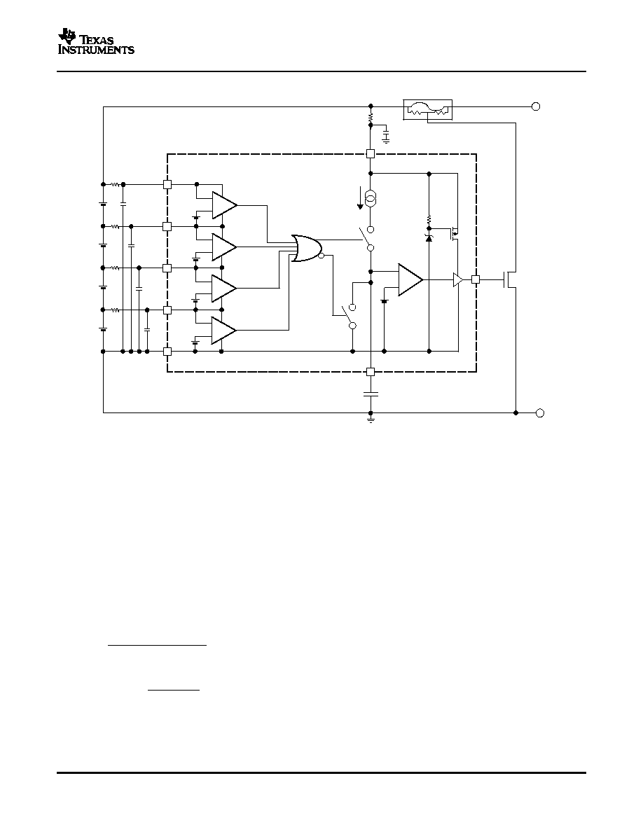
FUNCTIONAL BLOCK DIAGRAM
When one of the cell voltages exceeds V
(PROTECT)
, an internal current source begins to charge the capacitor,
C
(DELAY)
, connected to the CD pin. If the voltage at the CD pin, V
CD,
reaches 1.2 V, the OUT pin is activated and
transitions high. An externally connected NCH FET is activiated and blows the external fuse in the positive
battery rail; see the functional block diagram.
If all cell voltages fall below V
(PROTECT)
before the voltage at pin CD reaches 1.2 V, the delay time does not run
out. An internal switch clamps the CD pin to GND and discharges the capacitor, C
(DELAY)
, and secures the full
delay time for the next occurring overvoltage event.
Once the pin OUT is activated, it transitions back from high to low after all battery cells reach V
(PROTECT)
V
hys.
The delay time is calculated as follows:
Where I
(CD)
= CD current source = 0.18 µA
5
Document Outline