Document Outline
- FEATURES
- APPLICATIONS
- DESCRIPTION
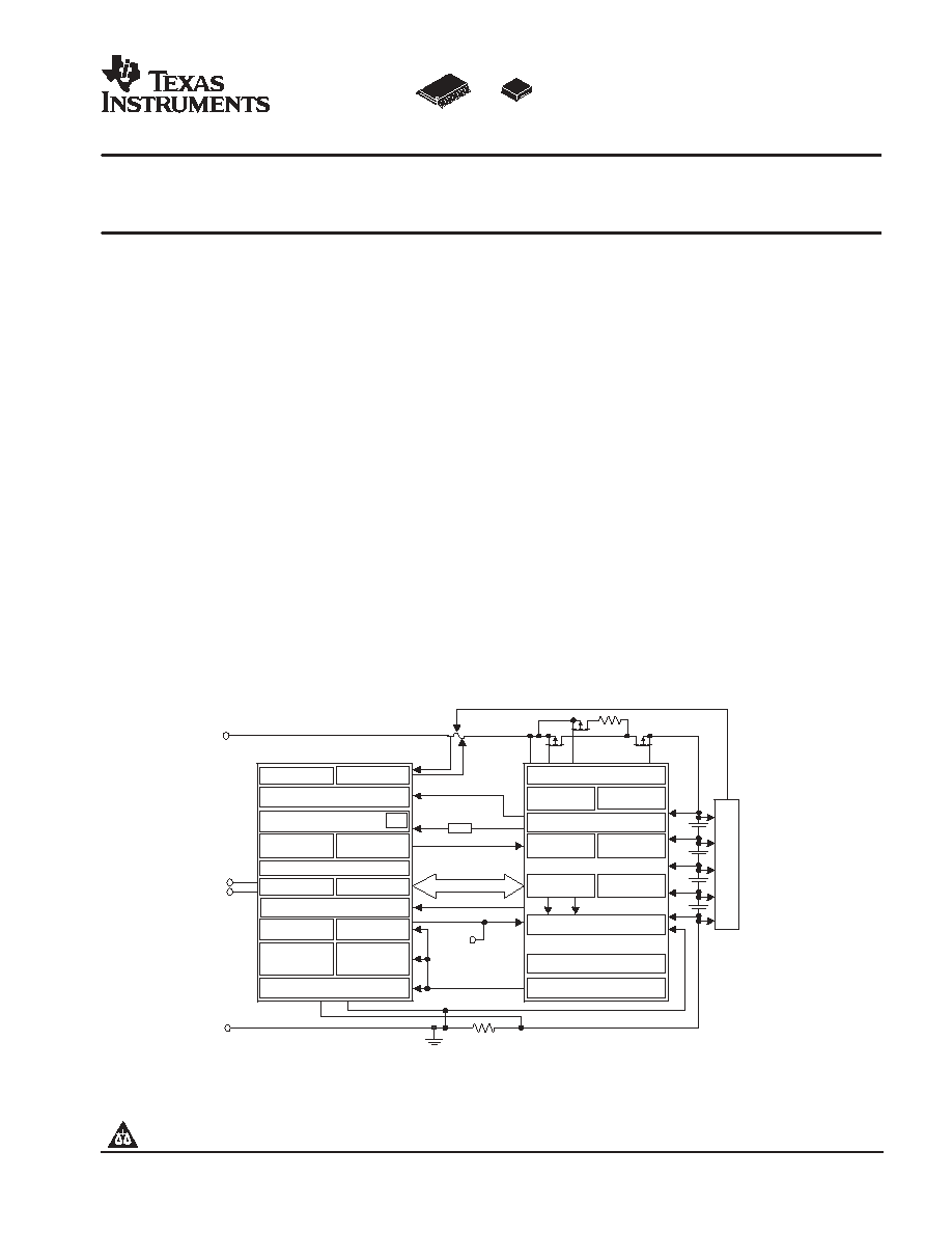
- SYSTEM PARTITIONING DIAGRAM
- ORDERING INFORMATION
- PACKAGE DISSIPATION RATINGS
- ABSOLUTE MAXIMUM RATINGS
- RECOMMENDED OPERATING CONDITIONS
- ELECTRICAL CHARACTERISTICS
- AC ELECTRICAL CHARACTERISTICS
- AC TIMING SPECIFICATIONS (I2C COMPATIBLE SERIAL INTERFACE)
- PIN ASSIGNMENTS
- Terminal Functions
- FUNCTIONAL BLOCK DIAGRAM
- STATE DIAGRAM
- FUNCTIONAL DESCRIPTION
- Low-Dropout Regulator (REG)
- Initialization
- Overload Detection
- Short-Circuit Detection
- Overload and Short-Circuit Delay
- Overload and Short-Circuit Response
- Cell Voltage
- Calibration of Cell Voltage Monitor Amplifier Gain
- Step 1
- Step 2
- Step 3
- Step 4
- Step 5
- Step 6
- Cell Balance Control
- Thermistor Drive Circuit (TOUT)
- Open Drain Drive Circuit (OD)
- XALERT (XALERT)
- Latch Clear (LTCLR)
- 2-, 3-, or 4-Cell Configuration
- Watchdog Input (WDI)
- DSG and CHG FET Driver Control
- Precharge and 0 V Charging„Theory of Operation
- SLEEP Control Input (SLEEP)
- Power Modes
- Communications
- Register Map
- STATUS : Status register
- OUTPUT CTL: Output Control Register
- STATE CTL: State Control Register
- FUNCTION CTL: Function Control Register
- CELL SEL: Cell Select Register
- OLV: Overload Voltage Threshold Register
- OLT: Overload Blanking Delay Time Register
- SCC: Short Circuit in Charge Configuration Register
- SCD: Short Circuit in Discharge Configuration Register
- APPLICATION INFORMATION
- PRECHARGE AND 0-V CHARGING„THEORY OF OPERATION
- 0-V Charge FET Mode
- Common FET
- Precharge FET
- Summary
- 0-V Charge FET (1) vs Common FET (2)
- 0-V Charge FET (1) vs Precharge FET (3)
- Precharge FET (3)
bq29312
SLUS546D - MARCH 2003 - REVISED SEPTEMBER 2004
THREE AND FOUR CELL LITHIUM ION OR
LITHIUM POLYMER BATTERY PROTECTION AFE
PW
RGE
FEATURES
D
2-, 3-, or 4-Cell Series Protection Control
D
Can Directly Interface With the bq2084 Gas
Gauges
D
Provides Individual Cell Voltages and Battery
Voltage to Battery Management Host
D
Integrated Cell Balancing Drive
D
I
2
C Compatible User Interface Allows Access
to Battery Information
D
Programmable Threshold and Delay for Over
Load and Short Circuit During Charge and
Discharge
D
System Alert Interrupt Output
D
Host Control Can Initiate Sleep Power Mode
and Ship Mode
D
Integrated 3.3-V, 25-mA LDO
D
Supply Voltage Range From 4.5 V to 25 V
D
Low Supply Current of 60-
µ
A Typical
APPLICATIONS
D
Notebook PCs
D
Medical and Test Equipment
D
Portable Instrumentation
DESCRIPTION
The bq29312 is a 2-, 3-, or 4-cell lithium-ion battery pack
protection analog front end (AFE) IC that incorporates a
3.3-V, 25-mA low-dropout regulator (LDO). The bq29312
also integrates an I
2
C compatible interface to extract
battery parameters such as cell voltages and control
output status. Other parameters such as current protection
thresholds and delays can be programmed into the
bq29312 to increase the flexibility of the battery
management system.
The bq29312 provides safety protection for overcharge,
overload, short-circuit, overvoltage, and undervoltage
conditions in conjunction with the battery management
host. In overload and short-circuit conditions, the bq29312
turns the FET drive off autonomously dependant on the
internal configuration setting.
SYSTEM PARTITIONING DIAGRAM
LDO, Therm Output Drive & UVLO
Power Management
LDO, TOUT and Power mode control
I2C
Capacity Prediction <1% Error
SMBus
Pack +
Pack -
Discharge / Charge /
Pre-Charge FETs
Cell and Pack
Voltage
Measurement
Pre-Charge
FET Drive
2-Tier Over Current Protection
32kHz Clock
Generator
bq2084
768 Bytes of
User Flash
Fuse
1st Level OV and
UV Protection
Pack Under Voltage
Power Mode
Control
Pre-charge Control
Delay Counters
Cell Balancing Algorithm and Control
Cell Balancing
Drive
System Interface
System Watchdog
Voltage Level Translator
System Interface
32kHz
Power Mode Control
Fail-Safe Protection
T1
1st Level OC
Protection
Temperature Measurement
<1% Error
TINT
Supply Voltage
bq29312
PCH FET Drive
RAM Registers
SBS v1.1 Data
bq29312 RAM/Comms Validation
2
n
d
Level Over V
oltage
Protection
XAlert
Sleep
Sense Resistor
(10 - 30 m
)
PF Input
PRODUCTION DATA information is current as of publication date. Products
conform to specifications per the terms of Texas Instruments standard warranty.
Production processing does not necessarily include testing of all parameters.
Please be aware that an important notice concerning availability, standard warranty, and use in critical applications of Texas Instruments
semiconductor products and disclaimers thereto appears at the end of this data sheet.
www.ti.com
Copyright
2004, Texas Instruments Incorporated
bq29312
SLUS546D - MARCH 2003 - REVISED SEPTEMBER 2004
www.ti.com
2
These devices have limited built-in ESD protection. The leads should be shorted together or the device placed in conductive foam during
storage or handling to prevent electrostatic damage to the MOS gates.
The communications inter-face allows the host to observe and control the current status of the bq29312. It enables cell
balancing, enters different power modes, sets overload levels, sets the over- load blanking delay time, sets short-circuit
threshold levels for charge and discharge, and sets the short-circuit blanking delay time.
Cell balancing of each cell is performed via a cell bypass path, which is enabled via the internal control register accessible
via the I
2
C compatible interface. The maximum bypass current is set via an external series resistor and internal FET on
resistance (typical 400
).
ORDERING INFORMATION
TA
PACKAGED
TA
TSSOP (PW)
QFN (RGE)
-25
°
C to 85
°
C
bq29312PW
bq29312PWR
bq29312RGE
bq29312RGER
PACKAGE DISSIPATION RATINGS
PACKAGE
POWER RATING
DERATING FACTOR
POWER RATING
PACKAGE
POWER RATING
TA
25
°
C
DERATING FACTOR
ABOVE TA
25
°
C
TA
70
°
C
TA = 85
°
C
PW
874 mW
6.99 W/
°
C
559 mW
454 mW
ABSOLUTE MAXIMUM RATINGS
over operating free-air temperature range unless otherwise noted(1)
bq29312
Supply voltage range
PACK, BAT
-0.3 V to 34 V
VC1, VC2, VC3, VC4
-0.3 V to 34 V
SR1, SR2
-1.0 V to 1.0 V
Input voltage range
VC5
-1.0 V to 4.0 V
Input voltage range
VC1 to VC2, VC2 to VC3, VC3 to VC4, VC4 to VC5
-0.3 to 8.5 V
WDI, SLEEP, SCLK, SDATA
-0.3 to 8.5 V
ZVCHG
-0.3 V to 34 V
DSG, CHG
-0.3 V to BAT
Output voltage range
OD
-0.3 V to 34 V
Output voltage range
PMS
-0.3 V to PACK-0.2 V
TOUT, SCLK, SDATA, CELL, XALERT
-0.3 to 7 V
Current for cell balancing
10 mA
Continuous total power dissipation
See Dissipation Rating Table
Storage temperature range, Tstg
-65
°
C to 150
°
C
Lead temperature (soldering, 10 sec)
300
°
C
(1) Stresses beyond those listed under "absolute maximum ratings" may cause permanent damage to the device. These are stress ratings only, and
functional operation of the device at these or any other conditions beyond those indicated under "recommended operating conditions" is not
implied. Exposure to absolute-maximum-rated conditions for extended periods may affect device reliability.
(2) All voltages are with respect to ground of this device except VCn-VC(n+1), where n=1, 2, 3, 4 cell voltage.

bq29312
SLUS546D - MARCH 2003 - REVISED SEPTEMBER 2004
www.ti.com
3
RECOMMENDED OPERATING CONDITIONS
MIN
NOM
MAX
UNIT
Supply Voltage (BAT or PACK)
4.5(1)
25
V
VI(STARTUP)
Start-up voltage (PACK)
5.0
V
VC1, VC2, VC3, VC4
0
BAT
SR1, SR2
-0.5
0.5
VI
Input voltage range
VC5
-0.5
3.0
V
VI
Input voltage range
VCn VC(n+1), (n=1, 2, 3, 4 )
0
5.0
V
PMS
0
PACK
SLEEP
0
REG
VIH
Logic level input voltage
SCLK, SDATA, WDI
0.8
×
REG
REG
V
VIL
Logic level input voltage
SCLK, SDATA, WDI
0
0.2
×
REG
VIH
PMS logic level
PMS
VPACK -0.2
VPACK
V
VIL
PMS logic level
PMS
0
0.2
PMS pull up/pull down resistance
RPMS
100
1000
k
VO
Output voltage
OD
25
V
IO
Output current
XALERT, SDATA
200
µ
A
II
Input current,
CELL
±
10
µ
A
II
Input current,
External 3.3 V REG capacitor
SLEEP
-0.5
1.0
µ
A
External 3.3 V REG capacitor
C(REG)
4.7
µ
F
Extend CELL output filter
R(CELL)
100
Extend CELL output filter
C(CELL)
100
nF
IOL
Input frequency
OD
1
mA
IOL
Input frequency
WDI
32.768
kHz
WDI high time
2
28
µ
s
TA
Operating temperature
-25
85
°
C
(1) V(PACK) supply voltage must rise above start-up voltage on power up to enable the internal regulator which drives REG and TOUT as required.
Once V(PACK) is above the start-up voltage, it can fall down to the minimum supply voltage and still meet the specifications of the bq29312.
bq29312
SLUS546D - MARCH 2003 - REVISED SEPTEMBER 2004
www.ti.com
4
ELECTRICAL CHARACTERISTICS
TA = 25
°
C, C(REG) = 4.7
µ
F, BAT = 14 V (unless otherwise noted)
PARAMETER
TEST CONDITIONS
MIN
TYP
MAX
UNIT
SUPPLY CURRENT
ICC1
Supply current 1
No load at REG, TOUT, XALERT, SCLK,
and SDATA. ZVCHG = off ,VMEN = on,
60
90
A
ICC1
Supply current 1
and SDATA. ZVCHG = off ,VMEN = on,
WDI no clock, Select VC5 = VC4 = 0 V
TA = -25
°
C to 85
°
C
100
µ
A
ICC2
Supply current 2
(Depends of VM
topology
selected)
No load at REG, TOUT, XALERT, SCLK,
and SDATA. ZVCHG = off, VMEN = off,
WDI no clock
TA = -25
°
C to 85
°
C
25
50
µ
A
I(SLEEP)
Sleep current
No load at REG, TOUT, XALERT, SCLK,
and SDATA.
CHG, DSG and ZVCHG = off, REG = on,
VMEN = off, WDI no clock,
SLEEP = REG or OPEN
TA = -25
°
C to 85
°
C
20
40
µ
A
I(SHIP)
Ship current
REG, CHG, DSG and ZVCHG = off,
REG = off, VMEN = off, WDI no clock,
VPACK= 0 V
TA = -25
°
C to 85
°
C
0.1
1.0
µ
A
3.3 V LDO
8.0 V< BAT or PACK
25 V, IOUT
25 mA
-4%
3.3
2%
V
6.5 V< BAT or PACK
8 V, IOUT
25 mA
-9%
3.3
2%
V
V(REG)
Regulator output
voltage
5.4 V
BAT or PACK
6.5 V,
IO
16 mA
TA =- 25
°
C to 85
°
C
-9%
3.3
2%
V
voltage
4.5 V
BAT or PACK
25 V,
IO
2 mA
-2%
3.3
2%
V
V(EGTEMP)
Regulator output
change with
temperature
5.4 V
BAT
25 V, IO = 2 mA,
TA =- 25
°
C to 85
°
C
±
0.2%
V(REGLINE)
Line regulation
5.4 V
BAT or PACK
25 V, IO = 2 mA
3
10
mV
V(REGLOAD) Load regulation
BAT = 14 V, 0.2 mA
IO
2 mA
7
15
mV
V(REGLOAD) Load regulation
BAT = 14 V, 0.2 mA
IO
25 mA
40
100
mV
IMAX
Current limit
BAT = 14 V, REG = 3.0 V
25
100
mA
IMAX
Current limit
BAT = 14 V, REG = 0 V
12
50
mA
CELL VOLTAGE MONITOR
V(CELL OUT)
CELL output
V(Cn) V(Cn + 1) = 0 V, 8.0 V
BAT or PACK
25 V
0.975
V
V(CELL OUT)
CELL output
V(Cn) V(Cn + 1) = 4.5 V, 8.0 V
BAT or PACK
25 V
0.3
V
REF
CELL output
Mode(1), 8.0 V
BAT or PACK
25 V
-1%
0.975
1%
V
PACK
CELL output
Mode(2)
-5%
PACK
/25
5%
V
K
CELL scale factor
K = {CELL output (VC5 = 0.0 V, VC4 = 4.5 V)
-CELL output (VC5 = VC4 = 0.0 V)/ 4.5
0.147
0.150
0.153
K
CELL scale factor
K = {CELL output (VC2 = 13.5 V, VC1 = 18.0 V)
-CELL output (VC2 = VC1 = 13.5 V)/ 4.5
0.147
0.150
0.153
VICR
CELL output
offset error
CELL output (VC2 = 17.0 V, VC1 = 17.0 V)
CELL output (VC2 = VC1 = 0.0 V)
-1
mV
R(BAL)
Cell balance
internal
resistance
rds(ON) for internal FET switch at VDS = 2.0 V
200
400
800
(1) Register Address =0x04, b2(CAL0) = b3(CAL1) = 1, Register Address = 0x03,b0(VMEN) = 1
(2) Register Address = 0x03, b1(PACKOUT) = 1, b0( VMEN) = 1
bq29312
SLUS546D - MARCH 2003 - REVISED SEPTEMBER 2004
www.ti.com
5
ELECTRICAL CHARACTERISTICS (Continued)
TA = 25
°
C, C(REG) = 4.7
µ
F, BAT = 14 V (unless otherwise noted)
PARAMETER
TEST CONDITION
MIN
NOM
MAX
UNIT
OVER LOAD (OL) AND SHORT CIRCUIT (SC) DETECTION
VOL
OL detection threshold range, typical(1)
-50
-205
mV
VOL
OL detection threshold program step
5
mV
VHYS(OL)
OL detection threshold hysteresis
7
10
13
mV
V(SC)
SC detection threshold range, typical(2)
Charge
100
475
mV
V(SC)
SC detection threshold range, typical(2)
Discharge
-100
-475
mV
V(SC)
SC detection threshold program step
Charge
25
mV
V(SC)
SC detection threshold program step
Discharge
-25
mV
VHYS(SC)
SC detection threshold hysteresis
Charge and Discharge
40
50
60
mV
(1)
VOL = 50 mV (min)
40
50
60
V(OL_acr)
OL detection threshold accuracy(1)
Discharge
VOL = 100 mV
90
100
110
mV
V(OL_acr)
OL detection threshold accuracy(1)
Discharge
VOL = 205 mV (max)
184
205
226
mV
(2)
Charge and
VSC = 100 mV (min)
80
100
120
V(SC_acr)
SC detection threshold accuracy(2)
Charge and
Discharge
VSC = 200 mV
180
200
220
mV
V(SC_acr)
SC detection threshold accuracy
Discharge
VSC = 475 mV (max)
426
475
523
mV
(1) See OL register for setting detection threshold
(2) See SC register for setting detection threshold
PARAMETER
TEST CONDITION
MIN
TYP
MAX
UNIT
FET DRIVE CIRCUIT
V(FETON)
Output voltage, charge and discharge
V(FETOND)= V(BAT) V(DSG)
VGS connect 1 M
BAT = 20 V
12
15
18
V
V(FETON)
Output voltage, charge and discharge
FETs on
V(FETONC)=V(PACK) V(CHG)
VGS connect 1 M
PACK = 20 V
12
15
18
V
V(ZCHG)
ZVCHG
clamp voltage
PACK = 4.5 V
3.3
3.5
3.7
V
V(FETOFF)
Output voltage, charge and discharge
V(FETOFF)= V(PACK) V(DSG) PACK = 16 V
0.2
V
V(FETOFF)
Output voltage, charge and discharge
FETs off
V(FETOFF)=V(BAT) V(CHG) BAT = 16 V
0.2
V
tr
Rise time
CL = 4700 pF
VDSG :10%-90%
40
200
s
tr
Rise time
CL = 4700 pF
VCHG :10%-90%
40
200
µ
s
tf
Fall time
CL = 4700 pF
VDSG :90%-10%
40
200
µ
s
tf
Fall time
CL = 4700 pF
VCHG :90%-10%
40
200
µ
s
PARAMETER
TEST CONDITION
MIN
NOM
MAX
UNIT
THERMISTOR DRIVE
rDS(on) TOUT pass-element series resistance
IO = -1 mA at TOUT pin, rds(ON) = (VREG VO
(TOUT))/1 mA, TA = -25
°
C to 85
°
C
50
100
PARAMETER
TEST CONDITION
MIN
NOM
MAX
UNIT
LOGIC
R(PUP) Internal pullup resistance
XALERT
TA = -25
°
C to 85
°
C
60
100
200
k
R(PUP) Internal pullup resistance
SDATA, SCLK,
TA = -25
°
C to 85
°
C
6
10
20
k
XALERT, IO = 200
µ
A,
TA = -25
°
C to 85
°
C
0.2
VOL
Logic level output voltage
SDATA, IO = 50
µ
A,
TA = -25
°
C to 85
°
C
0.4
V
VOL
Logic level output voltage
OD IO=1 mA,
TA = -25
°
C to 85
°
C
0.6
V
bq29312
SLUS546D - MARCH 2003 - REVISED SEPTEMBER 2004
www.ti.com
6
AC ELECTRICAL CHARACTERISTICS
TA = 25
°
C, C(REG) = 4.7
µ
F, BAT = 14 V (unless otherwise noted)
PARAMETER
TEST CONDITION
MIN
NOM
MAX
UNIT
t(WDTINT) WDT start-up detect time
250
700
2000
ms
t(WDWT) WDT detect time
100
µ
s
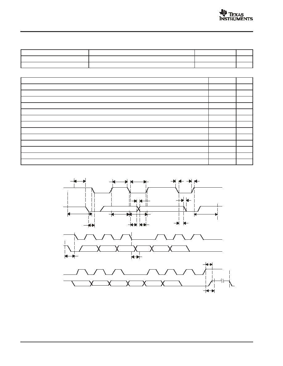
AC TIMING SPECIFICATIONS (I
2
C COMPATIBLE SERIAL INTERFACE)
PARAMETER
MIN
MAX
UNIT
tr
SCLK SDATA
r
ise time
1000
ns
tf
SCLK SDAT fall time
300
ns
tw(H)
SCLK pulse width high
4.0
µ
s
tw(L)
SCLK pulse width low
4.7
µ
s
tsu(STA)
Setup time for START condition
4.7
µ
s
th(STA)
START condition hold time after which first clock pulse is generated
4.0
µ
s
tsu(DAT)
Data setup time
250
ns
th(DAT)
Data hold time
0
µ
s
tsu(STOP)
Setup time for STOP condition
4.0
µ
s
tsu(BUF)
Time the bus must be free before new transmission can start
4.7
µ
s
t V
Clock low to data out valid
900
ns
th(CH)
Data out hold time after clock low
0
ns
fSCL
Clock frequency
0
100
kHz
tsu(STA)
SCLK
SDATA
SCLK
SDATA
SCLK
SDATA
tw(H)
tw(L)
tf
tr
tr
tf
Start
Condition
SDA
Input
SDA
Change
Stop
Condition
th(STA)
th(DAT)
tsu(DAT)
th(ch)
Start Condition
tv
1
2
3
7
8
9
MSB
ACK
Stop Condition
tsu(STOP)
1
2
3
7
8
9
MSB
ACK
tsu(BUF)
bq29312
SLUS546D - MARCH 2003 - REVISED SEPTEMBER 2004
www.ti.com
7
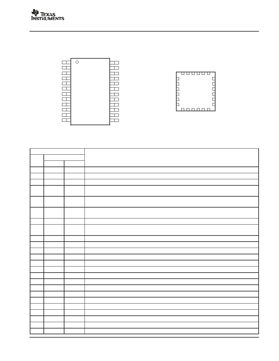
PIN ASSIGNMENTS
1
2
3
4
5
6
7
8
9
10
11
12
24
23
22
21
20
19
18
17
16
15
14
13
BAT
DSG
VC1
VC2
VC3
VC4
VC5
SR1
SR2
WDI
CELL
GND
OD
PMS
PACK
ZVCHG
CHG
SLEEP
REG
TOUT
XALERT
GND
SDATA
SCLK
PW PACKAGE
(TOP VIEW)
BA
T
DSG
VC1
VC3
VC4
SR2
SR1
VC5
GND
XALERT
REG
TOUT
ZVCHG
P
ACK
OD
WDI
CELL
SDA
T
A
GND
VC2
SCLK
SLEEP
CHG
PMS
RGE PACKAGE
(TOP VIEW)
Terminal Functions
TERMINAL
NO.
NAME
DESCRIPTION
NO.
QFN
PW
DESCRIPTION
1
VC2
BAT
Diode protected BAT+ terminal and primary power source.
2
VC3
DSG
Push-pull output discharge FET gate drive
3
VC4
VC1
Sense voltage input terminal for most positive cell and balance current input for most positive cell.
4
VC5
VC2
Sense voltage input terminal for second most positive cell, balance current input for second most positive cell
and return balance current for most positive cell.
5
SR1
VC3
Sense voltage input terminal for third most positive cell, balance current input for third most positive cell and
return balance current for second most positive cell.
6
SR2
VC4
Sense voltage input terminal for least positive cell, balance current input for least positive cell and return balance
current for third most positive cell.
7
WDI
VC5
Sense voltage input terminal for most negative cell, return balance current for least positive cell.
8
CELL
SR1
Current sense positive terminal when charging relative to SR2
Current sense negative terminal when discharging relative to SR2
9
GND
SR2
Current sense terminal
10
SCLK
WDI
Digital input that provides the timing clock for the OC and SC delays and also acts as the watchdog clock.
11
SDATA
CELL
Output of scaled value of the measured cell voltage.
12
GND
GND
Analog ground pin and negative pack terminal
13
XALERT
SCLK
Open-drain bidirectional serial interface clock with internal 10 k
pull-up to V(REG).
14
TOUT
SDATA
Open-drain bidirectional serial interface data with internal 10 k
pull-up to V(REG).
15
REG
GND
Connect to GND
16
SLEEP
XALERT
Open-drain output used to indicate status register changes. With internal 100 k
pull-up to V(REG)
17
CHG
TOUT
Provides thermistor bias current
18
ZVCHG
REG
Integrated 3.3-V regulator output
19
PACK
SLEEP
This pin is pulled up to V(REG) internally, open or H level makes Sleep mode
20
PMS
CHG
Push-pull output charge FET gate drive
21
OD
ZVCHG
The ZVCHG FET drive is connected here
22
BAT
PACK
PACK positive terminal and alternative power source
23
DSG
PMS
0-V charge configuration select pin, CHG terminal ON/OFF is determined by this pin.
24
VC1
OD
NCH FET open drain output
bq29312
SLUS546D - MARCH 2003 - REVISED SEPTEMBER 2004
www.ti.com
8
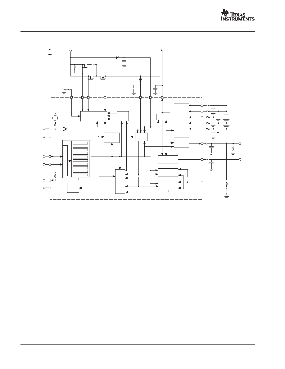
FUNCTIONAL BLOCK DIAGRAM
GND
CELL1..4
SR1
SR2
Over-Load
Comparator
Short Circuit
SHORT_CIRCUIT
DELAY
Open
Drain
Output
Watchdog
Timer
OD
Cell Voltage
Translation
Power
Mode
Circuit
Drive
Control
VCELL
R SNS
RCELL
CCELL
TOUT
R THERM
C THERM
THERMISTOR
Cell
Selection
Switches
3.3V LDO
POR
SHIP_ON
SLEEP_ON
BAT
PACK
REG
C (REG)
FET
Logic
Gate Driver
CHG_ON
DSG_ON
ZVCHG_ON
DSG
CHG
ZVCHG
PACK-
PACK+
R(ZVCHG)
PMS
GG VDD
VC1
VC2
VC5
CELL 3
CELL 4
VC3
VC4
CELL 1
CELL 2
GG TS
INPUT
GG ANALOG
INPUT
SLEEP
REG
WDI
SLEEP
CONTROL
32kHz INPUT
FROM GG
GG INTERFACE
SDATA
ALERT TO GG
OPEN DRAIN
OUTPUT
GG INTERFACE
SCLK
SDATA
SCLK
XALERT
SERIAL INTERF
ACE
Status
Output Ctl
State Ctl
Function Ctl
CELL_SEL
OCDV
OCDT
SCC
SCD
Registers
Comparator
OVER_CURRENT
REG
200 k
W
200 k
W
0.2
m
A
Current Source
_
+
-
bq29312
SLUS546D - MARCH 2003 - REVISED SEPTEMBER 2004
www.ti.com
9
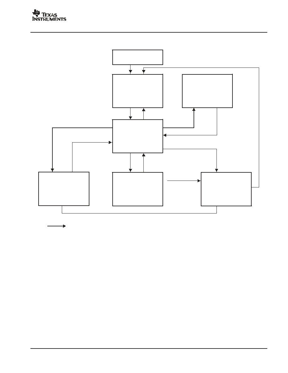
STATE DIAGRAM
No Power
POWER SUPPLY TO PACK
FETS: OFF(*2)
REG: start Working
I
2
C: OFF
CURRENT FAULT : OFF
CELL MONITOR : OFF
WATCHDOG : OFF
THERMISTOR PWER CTRL : OFF
INITIALIZE
FETS: OFF
REG: ON
I
2
C: ON
CURRENT FAULT : OFF
CELL MONITOR : OFF
WATCHDOG : ON
THERMISTOR PWER CTRL : OFF
HOST FAULT MODE
REG >2.4 V
REG < 2.3 V
FETS: ON *2
REG: ON
I
2
C: ON
CURRENT FAULT : ON
CELL MONITOR : ON
WATCHDOG : ON
THERMISTOR PWER CTRL : ON
NORMAL MODE
RESET WDTF LATCH
HOST CLOCK STOP
STATE CTL REGISTER b1 = 1
AND NO SUPPLY POWER TO PACK
FETS: OFF
REG: ON
I
2
C: ON
CURRENT FAULT : OFF
CELL MONITOR : OFF
WATCHDOG : OFF
THERMISTOR PWER CTRL : OFF
SLEEP MODE
SLEEP MODE EXIT BY
STATE CTL REGISTER b1 = 0
AND SLEEP PIN = GND
*1
FETS: OFF
REG: OFF
I
2
C: OFF
CURRENT FAULT : OFF
CELL MONITOR : OFF
WATCHDOG : OFF
THERMISTOR PWER CTRL : OFF
SHIP MODE
SHIP MODE SET BY STATE CTL REGISTER
b1 = 1 AND NO SUPPLY POWER TO PACK
FETS: OFF
REG: ON
I
2
C: ON
CURRENT FAULT : ON
CELL MONITOR : ON
WATCHDOG : ON
THERMISTOR PWER CTRL : ON
CURRENT DETECT MODE
STATE CTL REGISTER b0 = 1
or SLEEP PIN = REG or OPEN
*1
RESET CURRENT LATCH
IFAULT
SHIP MODE SET BY
STATE CTL REGISTER
b1 = 1 AND NO SUPPLY
POWER TO PACK
Interrupt Request When
Enrering These States
*1: Interrupt Request is Granted When Only External Sleep Pin Changes
*2: When PMS connect to Pack, Default State of CHG FET is ON.
SHIP MODE EXIT BY POWER
SUPPLY TO PACK

bq29312
SLUS546D - MARCH 2003 - REVISED SEPTEMBER 2004
www.ti.com
10
FUNCTIONAL DESCRIPTION
Low-Dropout Regulator (REG)
The inputs for this regulator can be derived from the battery cell stack (BAT) or the pack positive terminal (PACK). The output
is typically 3.3 V with the minimum output capacitance for stable operation is 4.7
µ
F and is also internally current limited.
During normal operation, the regulator limits output current to typically 50 mA.
Initialization
The bq29312 internal control circuit is powered by the REG voltage, which it also monitors. When the voltage at REG falls
below 2.3 V, the internal circuit turns off the FETs and disables all controllable functions, including the REG and TOUT
outputs. REG does not start up unless a voltage above V
(STARTUP)
is supplied to the PACK terminal. After the regulator
has started, based on PACK voltage, it keeps operating through the BAT input, even if the PACK voltage is removed. If
the BAT input is below the minimum operating range, then the bq29312 does not operate if the supply to the PACK input
is removed. After start up, when the REG voltage is above 2.4 V, the bq29312 is in Normal mode.
The initial state of the CHG output depends on the PMS input. If PMS = PACK then CHG = ON however, if PMS= GND
then CHG = OFF.
Overload Detection
The overload detection is used to detect abnormal currents in the discharge direction. This feature is used to protect the
pass FETs, cells and any other inline components from excessive current conditions. The detection circuit also incorporates
a blanking delay before driving the control for the pass FETs to the OFF state. The overload sense voltage is set in the OLV
register, and delay time is set in the OLT register. The overload threshold can be programmed from 50 mV to 205 mV in
5-mV steps with the default being 50 mV and hysteresis of 10 mV.
Short-Circuit Detection
The short current circuit detection is used to detect abnormal current in either the charge or discharge direction. This safety
feature is used to protect the pass FETs, cells, and any other inline components from excessive current conditions. The
detection circuit also incorporates a blanking delay before driving the control for the pass FETs to the OFF state. The short-
circuit thresholds and delay time are set in the SCC and SCD registers respectively where SCC is for charging and SCD
is for discharge. The short-circuit threshold can be programmed from 100 mV to 475 mV in 25-mV steps with the default
being 100 mV and hysteresis of 50 mV.
Overload and Short-Circuit Delay
The overload delay (default =1 ms) allows the system to momentarily accept a high current condition without disconnecting
the supply to the load. The delay time can be increased via the OLT register, which can be programmed for a range of 1
ms to 31 ms with steps of 2 ms.
The short-circuit delay (default = 0
µ
s) is programmable in the SCC and SCD registers. This register can be programmed
from 0
µ
s to 915
µ
s with steps of 61
µ
s.
Overload and Short-Circuit Response
When an overload or short-circuit fault is detected, the FETs are turned off. The STATUS (b0
...
b2) register reports the
details of short-circuit (charge), short-circuit (discharge), and overload. The respective STATUS (b0
...
b2) bits are set to
1 and the XALERT output is triggered. This condition is latched until the CONTROL (b0) is set and then reset. If a FET is
turned on via resetting CONTROL (b0) and the error condition is still present on the system, then the device reenters the
protection response state.
Cell Voltage
The cell voltage is translated to allow a system host to measure individual series elements of the battery. The series element
voltage is translated to a GND-based voltage equal to 0.15
±
0.002 of the series element voltage. This provides a range
from 0 V to 4.5 V. The translation output is inversely proportional to the input using the following equation.
Where, V
(CELL OUT)
= -K
×
V
(CELL IN)
+ 0.975 (V)
Programming CELL_SEL (b1, b0) selects the individual series element. The CELL_SEL (b3, b2) selects the voltage
monitor mode, cell monitor, offset etc.

bq29312
SLUS546D - MARCH 2003 - REVISED SEPTEMBER 2004
www.ti.com
11
Calibration of Cell Voltage Monitor Amplifier Gain
The cell voltage monitor amplifier has an offset and to increase accuracy this can be calibrated.
There are a couple of method by calibration circumstance.
The following procedure shows how to measure and calculate the offset and gain as one of example.
D
Step 1
-
Set CAL1=1, CAL0=1, CELL1=0, CELL0=0, VMEN=1
-
V
REF
is trimmed to 0.975 V within
±
1%, measuring V
REF
eliminates its error.
-
Measure internal reference voltage V
REF
from VCELL directly
.
-
VREF=measured reference voltage
D
Step 2
-
Set CAL1=0, CAL0=0, CELL1=0, CELL0=0, VMEN=1
-
The output voltage includes the offset and represented by:
V
O(4-5)
= V
REF
+ (1 + K)
×
V
OS
(V)
Where K = CELL Scaling Factor
-
V
OS
= Offset voltage at input of the internal Op-Amp
D
Step 3
-
Set CAL1=1, CAL0=0, CELL1=0, CELL0=0, VMEN=1
-
Measuring scaled REF voltage through VCELL amp.
-
The output voltage includes the scale factor error and offset and is represented by:
V
(OUTR)
= V
REF
+ (1 + K)
×
V
OS
K
×
V
REF
(V)
D
Step 4
-
Calculate (V
O(4-5)
-V
(OUTR
)/V
REF
-
The result will be the actual scaling factor, K
(ACT)
and is represented by:
-
K
(ACT)
= (V
O(4-5)
-V
(OUTR)
)/V
REF
= (V
REF
+ (1 + K)
×
V
OS
) - (V
REF
+ (1 + K)
×
V
OS
K
×
V
REF
)/
V
REF
= K
×
V
REF
/V
REF
= K
D
Step 5
-
Calculate the actual offset value where:
V
OS(ACT)
= (V
O(4-5)
V
REF
)/(1 + K
(ACT)
)
D
Step 6
-
Calibrated cell voltage is calculated by:
VCn VC(n+1) = { V
REF
+ (1 + K
(ACT)
)
×
V
OS(ACT)
V
(CELLOUT)
}
/K
(ACT) =
{V
O(4-5)
V
(CELLOUT)
}
/K
(ACT)
For improved measurement accuracy, V
OS(ACT)
for each cell voltage should be measured.
Set CAL1=0, CAL0=0, CELL1=0, CELL0=1, VMEN=1
Set CAL1=0, CAL0=0, CELL1=1, CELL0=0, VMEN=1
Set CAL1=0, CAL0=0, CELL1=1, CELL0=1, VMEN=1
Measuring V
O(3-4)
, V
O(2-3),
V
O(1-2),
VC4 VC5 = {V
O(4-5)
V(
CELLOUT)
}
/ K
(ACT)
VC3 VC4 = {V
O(3-4)
V
(CELLOUT)
}
/ K
(ACT)
VC2 VC3 = {V
O(2-3)
V
(CELLOUT)
}
/ K
(ACT)
VC1 VC2 = {V
O(1-2)
V
(CELLOUT)
}
/ K
(ACT)
bq29312
SLUS546D - MARCH 2003 - REVISED SEPTEMBER 2004
www.ti.com
12
Cell Balance Control
The cell balance control allows a small bypass path to be controlled for any one series element. The purpose of this bypass
path is to reduce the current into any one cell during charging to bring the series elements to the same voltage. Series
resistors placed between the input pins and the positive series element nodes control the bypass current value. Individual
series element selection is made using bits 4 through 7 of the CELL_SEL register.
Thermistor Drive Circuit (TOUT)
The TOUT pin can be enabled to drive a thermistor from REG. The typical thermistor resistance is 10 k
at 25
°
C. The
default-state is OFF to conserve power. The maximum output impedance is 100
. TOUT is enabled in FUNCTION CTL
Register (bit 5).
Open Drain Drive Circuit (OD)
The open drain output has 1-mA current source drive with a maximum output voltage of 25 V. The OD output is enabled
or disabled by OUTPUT CTL Register (bit 4) and has a default state of OFF.
XALERT (XALERT)
XALERT is driven low when an OL or SC current fault is detected, if the SLEEP pin changes state or a watchdog fault
occurs. To clear XALERT, toggle (from 0, set to 1 then reset to 0) OUTPUT CTL (bit 0), then read the STATUS register.
Latch Clear (LTCLR)
When a current limit fault or watch dog timer fault occurs, the state is latched. To clear these faults, toggle (from 0, set 1
then reset to 0) LTCLR in the OUTPUT CTL register (bit 0).
Figure 1 is the LTCLR and XALERT clear example after sensing short-circuit.
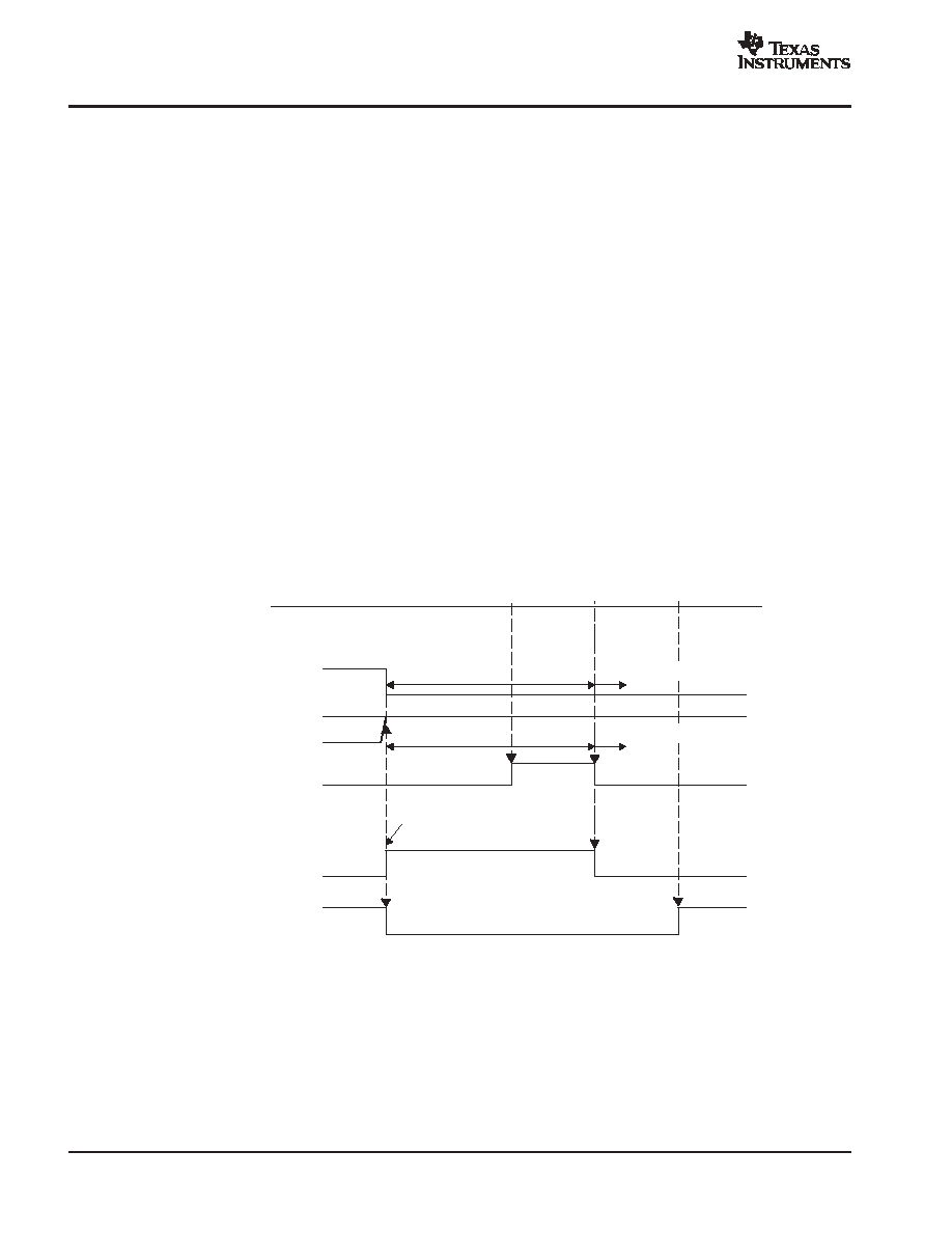
I2C
OUTPUT CTRL (b3)
XZVCHG
OUTPUT CTRL (b2-b1)
DSG, CHG
OUTPUT CTRL (b0)
LTCLR
STATUS (b0)
SCDSG
XALERT Pin
LTCLR
Write = 1
LTCLR
Write = 0
Read STATUS
Register
Access Enable
Access Enable
Access Enable
Short Current Timeout
in Discharge Direction
Staied Disable
Staied Disable
Figure 1. LTCLR and XALERT Clear Example After Sensing Short LTCLR and XALER Clear Example
2-, 3-, or 4-Cell Configuration
In a 3-cell configuration, VC1 is shorted to VC2. In a 2-cell configuration, VC1 and VC2 are shorted to VC3.

bq29312
SLUS546D - MARCH 2003 - REVISED SEPTEMBER 2004
www.ti.com
13
Watchdog Input (WDI)
The WDI input is required as a time base for delay timing when determining overload and short-circuit delay periods and
is used as part of the system watchdog.
Initially the watchdog monitors the hosts oscillator start up, if there is no response from the host within 700 ms of the
bq29312 reaching its minimum operating voltage, then the bq29312 turns both CHG, DSG and ZVCHG FETs OFF.
Once the watchdog has been started during this wake up period, it monitors the host for an oscillation stop condition, which
is defined as a period of 100
µ
s (typ) where no clock input is received. If an oscillator stop condition is identified, then the
watchdog turns the CHG, DSG and ZVCHG FETs OFF. When the host clock oscillation is started, WDF is released, but
the flag is latched until LTCLR is toggled.
GG Clock Never Starts
REG
GG 32 kHz Output
tWDTINT
700 mS
CHG, DSG and
ZVCHG = OFF
EXT FET Control
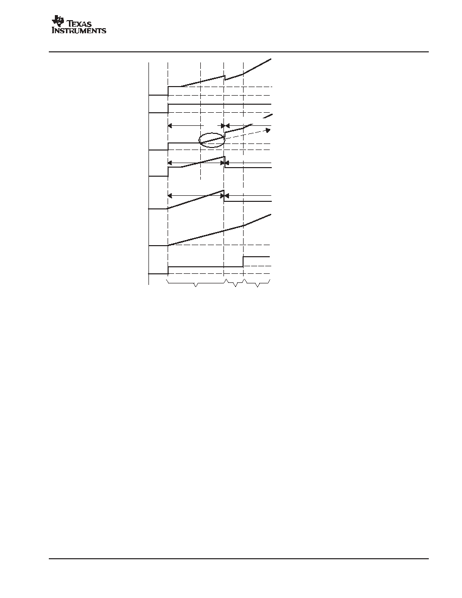
Figure 2. Watchdog Timing Chart--WDI Fault at Startup
GG Clock Stop
CHG, DSG and
ZVCHG = OFF
tWDWT About 100
µ
S
REG
GG 32 kHz Output
Watchdog Sense
EXT FET Control
Figure 3. Watchdog Timing Chart--WDI Fault After Startup

bq29312
SLUS546D - MARCH 2003 - REVISED SEPTEMBER 2004
www.ti.com
14
DSG and CHG FET Driver Control
The bq29312 drives the DSG, CHG, and ZVCHG FET off if an OL or SC safety threshold is breached depending on the
current direction. The host can force any FET on or off only if the bq29312 integrated protection control allows. The DSG
and CHG FET drive gate-to-drain voltage is clamped to 15 V (typ).
The default-state of the CHG and DSG FET drive is off, when PMS = GND. A host can control the FET drive by
programming OUTPUT CTL (b3...b1) where b1 is used to control the discharge FET, b2 is used to control the charge FET
and b3 is used to control the ZVCHG FET. These controls are only valid when not in the initialized state. The CHG drive
FET can be powered by PACK and the DSG FET can be powered by BAT.
Precharge and 0 V Charging--Theory of Operation
The bq29312 supports both a charger that has a precharge mode and one that doesn't. The bq29312 also supports
charging even when the battery falls to 0 V. Detail is described in the application section.
SLEEP Control Input (SLEEP)
The SLEEP input is pulled-up internally to REG. When SLEEP is pulled to REG, the bq29312 enters the SLEEP mode.
The SLEEP mode disables all the FET outputs and the OL, SC and watchdog faults are also disabled. The RAM
configuration is still valid on exit of the SLEEP mode. The host can force the bq29312 into SLEEP mode via register control
also.
ITEM
SLEEP
EXIT SLEEP
ITEM
FUNCTION
I2C READ/WRITE
EXIT SLEEP
I2C Read/Write
Active
REG Output
Active
External pin control:
CHG, DSG, ZVCHG, TOUT, OD
OC and SC protection:
SCD, SCC and OCD
CELL Translation
PACKOUT, VMEN
Cell Balancing:
CB[3:0]
Watchdog: WDDIS
Disabled
Write is available, but read is disabled
Last pre-sleep entry configuration is valid.
(If change configuration, latest write data is
valid.)
Power Modes
The bq29312 has three power modes, Normal, Sleep, and Ship. The following table outlines the operational functions
during these power modes.
POWER
MODE
TO ENTER POWER MODE
TO EXIT POWER MODE
MODE DESCRIPTION
Normal
SLEEP = GND and
STATE CTL( b0) = 0 and
STATE CTL( b1) = 0
The battery is in normal operation with protection, power
management and battery monitoring functions available and
operating.
The supply current of this mode varies as the host can enable and
disable various power management features.
Sleep
{SLEEP = REG (floating) or
STATE CTL( b0) = 1 } and
STATE CTL( b1) = 0
SLEEP = GND and
STATE CTL( b0) = 0
All functions stop except LDO and I2C interface.
On entry to this mode, all registers are masked off keeping their
state.
The host controller can change the RAM registers via the I2C
interface, but reading data is disabled until exit of Sleep mode.
Ship
STATE CTL( b1) = 1
And supply at the PACK pin is
removed
Supply voltage to PACK
The bq29312 is completely shut down as in the sleep mode. In
addition the REG output is disabled, I2C interface is powered
down and memory is not valid.

bq29312
SLUS546D - MARCH 2003 - REVISED SEPTEMBER 2004
www.ti.com
15
Communications
The I
2
C compatible serial communications provides read and write access to the bq29312 data area. The data is clocked
via separate data (SDATA) and clock (SCLK) pins. The bq29312 acts as a slave device and does not generate clock pulses.
Communication to the bq29312 is provided from GPIO pins or an I
2
C supporting port of a host system controller. The slave
address for the bq29312 is 7 bits and the value is 0100 000 (0x20).
(MSB)
I2C ADDRESS +R/W BIT
(LSB)
(MSB)
I2C ADDRESS (0X20)
(LSB)
Write
0
1
0
0
0
0
0
0
Read
0
1
0
0
0
0
0
1
NOTE: Bit 0: 0 = write, 1= read
The bq29312 does not have the following functions compatible with the I
2
C specification.
D
The bq29312 is always regarded as a slave.
D
The bq29312 does not return a NACK for an invalid register address.
D
The bq29312 does not support the general code of the I
2
C specification, and therefore does not return an ACK.
D
The bq29312 does not support the address auto increment, which allows continuous reading and writing.
D
The bq29312 allows data to written or read from the same location without resending the location address.
A5
SCLK
SDATA
A6
ACK
R/W
A0
A4
R5
R6
R7
R0
D7
ACK
D6
D5
D0 ACK
0
0
0
0
...
...
...
...
...
...
Slave Address
Register Address
Data
Start
Stop
Note: Slave = bq29312
Figure 4. I
2
C-Bus Write to bq29312
A5
SCLK
SDATA
Stop
A6
ACK
R/W
A0
R6
R7
R0
A6
ACK
A0
R/W
ACK
D7
0
1
0
D6
D0 NACK
...
...
...
...
...
...
...
0
0
Slave Address
Register Address
Data
Start
Note: Slave = bq29312
Slave Address
Slave Drives
The Data
Master Drives
NACK and Stop
Figure 5. I
2
C-Bus Read from bq29312: Protocol A
A5
SCLK
SDATA
Stop
A6
ACK
R/W
A0
R6
R7
R0
A6
ACK
A0
R/W ACK
D7
0
0
0
D0 NACK
A5
Stop Start
...
...
...
...
...
...
...
...
Slave Address
Register
Address
Start
Note: Slave = bq29312
Slave Address
Slave Drives
The Data
Master Drives
NACK and Stop
Figure 6. I
2
C-Bus Read from bq29312: Protocol B

bq29312
SLUS546D - MARCH 2003 - REVISED SEPTEMBER 2004
www.ti.com
16
Register Map
The bq29312 has 9 addressable registers. These registers provide status, control, and configuration information for the
battery protection system.
NAME
ADDR
TYPE
DESCRIPTION
STATUS
0x00
R
Status register
OUTPUT CTL
0x01
R/W
Output pin control from system host
STATE CTL
0x02
R/W
State control
FUNCTION CTL
0x03
R/W
Function control
CELL _SEL
0x04
R/W
Battery cell select for cell translation and balance bypass and select mode for calibration
OLV
0x05
R/W
Overload threshold voltage
OLT
0x06
R/W
Overload delay time
SCC
0x07
R/W
Short-circuit current threshold voltage and delay for charge
SCD
0x08
R/W
Short-circuit current threshold voltage and delay for discharge
STATUS : Status register
STATUS REGISTER (0X00)
7
6
5
4
3
2
1
0
0
0
ZVCLMP
SLEEPDET
WDF
OL
SCCHG
SCDSG
The STATUS register provides information about the current state of the bq29312. Reading the STATUS register clears
the XALERT pin.
STATUS b0 (SCDSG): This bit indicates a short-circuit in the discharge direction.
0 = Current below the short-circuit threshold in the discharge direction (default).
1 = Current greater than or equal to the short-circuit threshold in the discharge direction.
STATUS b1 (SCCHG): This bit indicates a short-circuit in the charge direction.
0 = Current below the short-circuit threshold in the charge direction (default).
1 = Current greater than or equal to the short-circuit threshold in the charge direction.
STATUS b2 (OL): This bit indicates an overload condition.
0 = Current less than or equal to the overload threshold (default).
1 = Current greater than overload threshold.
STATUS b3 (WDF): This bit indicates a watchdog fault condition has occurred.
0 = 32kHz oscillation is normal (default).
1 = 32kHz oscillation stopped or not started and the watchdog has timed out.
STATUS b4 (SLEEPDET): This bit indicates the bq29312 is SLEEP mode
0 = bq29312 is not SLEEP mode (default).
1 = bq29312 is SLEEP mode.
STATUS b5 (ZVCLMP): This bit indicates ZVCHG output is clamped.
0 = ZVCHG pin is not clamped (default).
1 = ZVCHG pin is clamped.

bq29312
SLUS546D - MARCH 2003 - REVISED SEPTEMBER 2004
www.ti.com
17
OUTPUT CTL: Output Control Register
OUTPUT CTL REGISTER (0X01)
7
6
5
4
3
2
1
0
0
0
0
OD
XZVCHG
CHG
DSG
LTCLR
The OUPTU CTL register controls the outputs of the bq29312 and can be used to clear certain states.
OUTPUT CTL b0 (LTCLR): When a current limit fault or watchdog timer fault is latched, this bit releases the fault latch when
toggled from 0 to 1 and back to 0 (default =0).
0 = (default)
0->1 ->0 clears the fault latches
OUTPUT CTL b1 (DSG): This bit controls the external discharge FET.
0 = discharge FET is off and is controlled by the system host (default).
1 = discharge FET is on and the bq29312 is in normal operating mode.
OUTPUT CTL b2 (CHG): This bit controls the external charge FET.
PMS=GND
0 = charge FET is off and is controlled by the system host (default).
1 = charge FET is on and the bq29312 is in normal operating mode.
PMS=PACK
0 = charge FET is off and is controlled by the system host.
1 = charge FET is on and the bq29312 is in normal operating mode (default).
OUTPUT CTL b3 (XZVCHG): This bit controls the external ZVCHG FET.
0 = ZVCHG FET is on and is controlled by the system host (default).
1 = ZVCHG FET is off and the bq29312 is in normal operating mode.
OUTPUT CTL b4 (OD): This bit enables or disables the OD output.
0 = OD is high impedance (default).
1 = OD output is active (GND).
STATE CTL: State Control Register
STATE CTL REGISTER (0X02)
7
6
5
4
3
2
1
0
0
0
0
0
0
WDDIS
SHIP
SLEEP
The STATE CTL register controls the state of the bq29312.
STATE CTL b0 (SLEEP): This bit is used to enter the sleep power mode.
0 = bq29312 exits sleep mode (default).
1 = bq29312 enters the sleep mode.
STATE CTL b1 (SHIP): This bit is used to enter the ship power mode when pack supply voltage is not applied.
0 = bq29312 in normal mode (default).
1 = bq29312 enters ship mode when pack voltage is removed.
STATE CTL b2 (WDDIS): This bit is used to enable or disable the watchdog timer function.
0 = enable clock monitoring (default).
1 = disable clock monitoring.
NOTE: Use caution when setting the WDDIS. For example, when the 32-kHz input fails, the overload and short-circuit delay timers no longer function
because they use the same WDI input. If the WDI input clock stops, these current protections do not function. WDF should be enabled at
any time for maximum safety. If the watchdog function is disabled, the CHG and DSG FETs should be turned off.

bq29312
SLUS546D - MARCH 2003 - REVISED SEPTEMBER 2004
www.ti.com
18
FUNCTION CTL: Function Control Register
FUNCTION CTL REGISTER (0X03)
7
6
5
4
3
2
1
0
0
0
TOUT
XSCD
SSCC
XOL
PACKOUT
VMEN
The FUNCTION CTL register enables and disables functons of the bq29312.
FUNCTION CTL b0 (VMEN): This bit enables or disables the cell and battery voltage monitoring function.
0 = disable voltage monitoring (default). CELL output is pulled down to GND level.
1 = enable voltage monitoring.
FUNCTION CTL b1 (PACKOUT): This bit is used to translate the PACK input to the CELL pin when VMEN=1
The pack voltage is divided by 25 and is presented on CELL regardless of the CELL_SEL register settings.
0 = disable PACK OUT (default).
1 = enable PACK OUT.
FUNCTION CTL b2 (XOL): This bit enables or disables the over current sense function.
0 = enable over load sense (default).
1 = disable over load sense.
FUNCTION CTL b3 (XSCC): This bit enables or disables the short current sense function of charging.
0 = enable short-circuit current sense in charge direction (default).
1 = disable short-circuit current sense in charge direction.
FUNCTION CTL b4 (XSCD): This bit enables or disables the short current sense function of discharge
0 = enable short-circuit current sense in discharge direction (default).
1 = disable short-circuit current sense in discharge direction.
FUNCTION CTL b5 (TOUT): This bit controls the power to the thermistor.
0 = thermistor power is off (default).
1 = thermistor power is on.

bq29312
SLUS546D - MARCH 2003 - REVISED SEPTEMBER 2004
www.ti.com
19
CELL SEL: Cell Select Register
CELL_SEL REGISTER (0X04)
7
6
5
4
3
2
1
0
CB3
CB2
CB1
CB0
CAL1
CAL0
CELL1
CELL0
This register determines cell selection for voltage measurement and translation, cell balancing and the operational mode
of the cell voltage monitoring.
CELL_SEL b0-b1 (CELL0 CELL1): These two bits select the series cell for voltage measurement translation.
CELL1
CELL0
SELECTED CELL
0
0
VC4-VC5, Bottom series element (Default)
0
1
VC4-VC3, Second lowest series element
1
0
VC3-VC2, Second highest series element
1
1
VC1-VC2, Top series element
CELL_SEL b2-b3 (CAL1, CAL0): These bits determine the mode of the voltage monitor block.
CAL1
CAL0
SELECTED MODE
0
0
Cell translation for selected cell (default)
0
1
Offset measurement for selected cell
1
0
Monitor the VREF value for gain calibration
1
1
Monitor the VREF directly value for gain calibration, bypassing the translation circuit
CELL_SEL b4-b7 (CB0 CB3): These 4 bits select the series cell for cell balance bypass path.
CELL SEL b4 (CB0): This bit enables or disables the bottom series cell balance charge bypass path
0 = disable bottom series cell balance charge bypass path (default).
1 = enable bottom series cell balance charge bypass path.
CELL SEL b5 (CB1): This bit enables or disables the second lowest series cell balance charge bypass path.
0 = disable series cell balance charge bypass path (default).
1 = enable series cell balance charge bypass path.
CELL SEL b6 (CB2): This bit enables or disables the second highest cell balance charge bypass path.
0 = disable series cell balance charge bypass path (default).
1 = enable series cell balance charge bypass path.
CELL SEL b7 (CB3): This bit enables or disables the highest series cell balance charge bypass path.
0 = disable series cell balance charge bypass path (default).
1 = enable series cell balance charge bypass path.

bq29312
SLUS546D - MARCH 2003 - REVISED SEPTEMBER 2004
www.ti.com
20
OLV: Overload Voltage Threshold Register
OLV REGISTER (0X05)
7
6
5
4
3
2
1
0
0
0
0
OLV4
OLV3
OLV2
OLV1
OLV0
OLV (b4-b0): These five bits select the value of the over load threshold with a default of 00000.
OLV (b4-b0) configuration bits with corresponding voltage threshold
00000
0.050 V
01000
0.090 V
10000
0.130 V
11000
0.170 V
00001
0.055 V
01001
0.095 V
10001
0.135 V
11001
0.175 V
00010
0.060 V
01010
0.100 V
10010
0.140 V
11010
0.180 V
00011
0.065 V
01011
0.105 V
10011
0.145 V
11011
0.185 V
00100
0.070 V
01100
0.110 V
10100
0.150 V
11100
0.190 V
00101
0.075 V
01101
0.115 V
10101
0.155 V
11101
0.195 V
00110
0.080 V
01110
0.120 V
10110
0.160 V
11110
0.200 V
00111
0.085 V
01111
0.125 V
10111
0.165 V
11111
0.205 V
OLT: Overload Blanking Delay Time Register
OLT REGISTER (0X06)
7
6
5
4
3
2
1
0
0
0
0
0
OLT3
OLT2
OLT1
OLT0
OLT(b3-b0): These four bits select the value of the delay time for overload with a default of 0000.
OLT(b3-b0) configuration bits with corresponding delay time
0000
1 ms
0100
9 ms
1000
17 ms
1100
25 ms
0001
3 ms
0101
11 ms
1001
19 ms
1101
27 ms
0010
5 ms
0110
13 ms
1010
21 ms
1110
29 ms
0011
7 ms
0111
15 ms
1011
23 ms
1111
31 ms
SCC: Short Circuit in Charge Configuration Register
SCC REGISTER (0X07)
7
6
5
4
3
2
1
0
SCCT3
SCCT2
SCCT1
SCCT0
SCCV3
SCCV2
SCCV1
SCCV0
This register selects the short-circuit threshold voltage and delay for charge.
SCC(b3-b0) : These bits select the value of the short-circuit voltage threshold with 0000 as the default.
SCC(b3-b0) with corresponding SC threshold voltage
0000
0.100 V
0100
0.200 V
1000
0.300 V
1100
0.400 V
0001
0.125 V
0101
0.225 V
1001
0.325 V
1101
0.425 V
0010
0.150 V
0110
0.250 V
1010
0.350 V
1110
0.450 V
0011
0.175 V
0111
0.275 V
1011
0.375 V
1111
0.475 V
SCC(b7-b4): These bits select the value of the short-circuit delay time. Exceeding the short-circuit voltage threshold for
longer than this period will turn off the corresponding CHG, DSG, and ZVCHG output. 0000 is the default.
SCC(b7-b4) with corresponding SC delay time
0000
0
µ
s
0100
244
µ
s
1000
488
µ
s
1100
732
µ
s
0001
61
µ
s
0101
305
µ
s
1001
549
µ
s
1101
793
µ
s
0010
122
µ
s
0110
366
µ
s
1010
610
µ
s
1110
854
µ
s
0011
183
µ
s
0111
427
µ
s
1011
671
µ
s
1111
915
µ
s
bq29312
SLUS546D - MARCH 2003 - REVISED SEPTEMBER 2004
www.ti.com
21
SCD: Short Circuit in Discharge Configuration Register
SCD REGISTER (0X08)
7
6
5
4
3
2
1
0
SCDT3
SCDT2
SCDT1
SCDT0
SCDV3
SCDV2
SCDV1
SCDV0
This register selects the short-circuit threshold voltage and delay for discharge.
SCD(b3-b0) with corresponding SC threshold voltage with 0000 as the default.
SCD(b3-b0): These bits select the value of the short-circuit voltage threshold
0000
0.10 V
0100
0.20 V
1000
0.30 V
1100
0.40 V
0001
0.125 V
0101
0.225 V
1001
0.325 V
1101
0.425 V
0010
0.150 V
0110
0.250 V
1010
0.350 V
1110
0.450 V
0011
0.175 V
0111
0.275 V
1011
0.375 V
1111
0.475 V
SCD(b7-b4): These bits select the value of the short-circuit delay time. Exceeding the short-circuit voltage threshold for
longer than this period will turn off the corresponding CHG, DSG, and ZVCHG output as has 0000 as the default.
SCD(b7-b4) with corresponding SC delay time
0000
0
µ
s
0100
244
µ
s
1000
488
µ
s
1100
732
µ
s
0001
61
µ
s
0101
305
µ
s
1001
549
µ
s
1101
793
µ
s
0010
122
µ
s
0110
366
µ
s
1010
610
µ
s
1110
854
µ
s
0011
183
µ
s
0111
427
µ
s
1011
671
µ
s
1111
915
µ
s
bq29312
SLUS546D - MARCH 2003 - REVISED SEPTEMBER 2004
www.ti.com
22
APPLICATION INFORMATION
PRECHARGE AND 0-V CHARGING--THEORY OF OPERATION
In order to charge, the charge FET (CHG-FET) must be turned on to create a current path. When the V
(BAT)
is 0 V and
CHG-FET = ON, the V
(PACK)
is as low as the battery voltage. In this case, the supply voltage for the device is too low to
operate. There are 3 possible configurations for this function and the bq29312 can be easily configured according to the
application needs. The 3 modes are 0-V Charge FET Mode, Common FET Mode and Precharge FET Mode.
1.
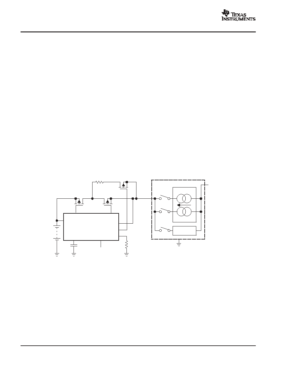
0-V Charge FET Mode - Dedicates a precharge current path using an additional FET (ZVCHG-FET) to sustain
the PACK+ voltage level. The host charger is expected to provide a precharge function.
2.
Common FET Mode - Does not use a dedicated precharge FET. The charge FET (CHG-FET) is assured to be
set to ON state as default. The charger is expected to provide a precharge function.
3.
Precharge FET Mode - Dedicates a precharge current path using an additional open drain (OD) pin drive FET
(PCHG-FET) FET to sustain the PACK+ voltage level. The charger does not provide any precharge function.
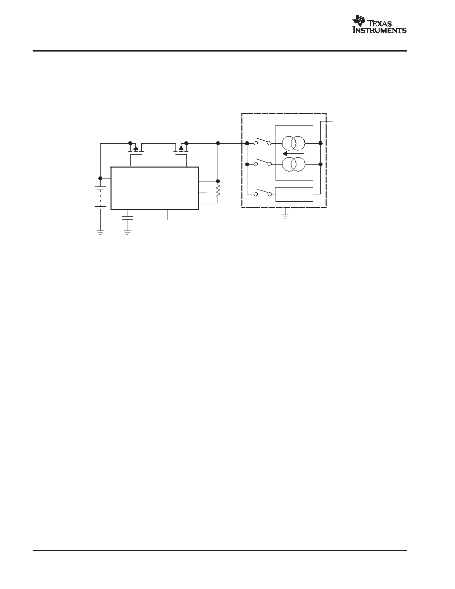
0-V Charge FET Mode
In this mode, a dedicated precharge current path using an additional FET (ZVCHG-FET) is required to sustain a suitable
PACK+ voltage level. The charger is expected to provide the precharge function in this mode where the precharge current
level is suitable to charge cells below a set level, typically below 3 V per cell. When the lowest cell voltage rises above this
level, then a fast charging current is applied by the charger.
The circuit diagram for this method is shown in Figure 7, showing how the additional FET is added in parallel with the charge
FET (CHG-FET).
PACK
ZVCHG
PMS
REG
CHG
DSG
BAT
ZVCHG-FET
R(ZVCHG)
4.7
µ
F
Battery
DSG-FET
CHG-FET
Pack+
IZVCHG
IFASTCHG
CV
CC
Charger
DC Input
bq29312
I(ZVCHG) = 0 V Percharge Current
I(FASTCHG) = Fast Current
OD
NC
Figure 7. 0-V Charge FET Mode Circuit

bq29312
SLUS546D - MARCH 2003 - REVISED SEPTEMBER 2004
www.ti.com
23
In order to pass 0 V or precharge current an appropriate gate-source voltage V
(GS)
, for ZVCHG-FET must be applied. Here,
V
(PACK)
can be expressed in terms of V
(GS)
as follows:
V
(PACK)
= V
(ZVCHG)
+ V
(GS)
(ZVCHG-FET gate source voltage)
VDS
Precharge
Current
ID
VGS
Point A
Point B
Figure 8. Drain Current vs Drain-Source Voltage Characteristics
In the bq29312, the initial state is for CHG-FET = OFF and ZVCHG-FET = ON with the V
(ZVCHG)
clamped at 3.5 V initially.
Then the charger applies a constant current and raises V
(PACK)
high enough to pass the precharge current, point A. For
example, if the V
(GS)
is 2 V at this point, V
(PACK)
is 3.5 V + 2 V = 5.5 V. Also, the ZVCHG-FET is used in its MOS saturation
region at this point so that V
(DS)
is expressed as follows:
V
(PACK)
= V
(BAT)
+ V
F
+ V
DS(ZVCHG-FET)
where V
(F)
= 0.7 V is the forward voltage of a DSG-FET back diode and is typically 0.7 V.
This derives the following equation:
V
DS
= 4.8 V V
(BAT)
As the battery is charged V
(BAT)
increases and the V
(DS)
voltage decreases reaching its linear region. For example: If the
linear region is 0.2 V, this state continues until V
(BAT)
= 4.6 V, (4.8 V 0.2 V).
As V
(BAT)
increases further, V
(PACK)
and the V
(GS)
voltage increase. But the V
DS
remains at 0.2 V because the ZVCHG-FET
is driven in its MOS linear region, point B.
V
(PACK)
= V
F
+ 0.2 V +
V(BAT)
where V
F
= 0.7 V is the forward voltage of a DSG-FET back diode and is typically 0.7 V
The R
(ZVCHG)
purpose is to split heat dissipation across the ZVCHG-FET and the resistor.
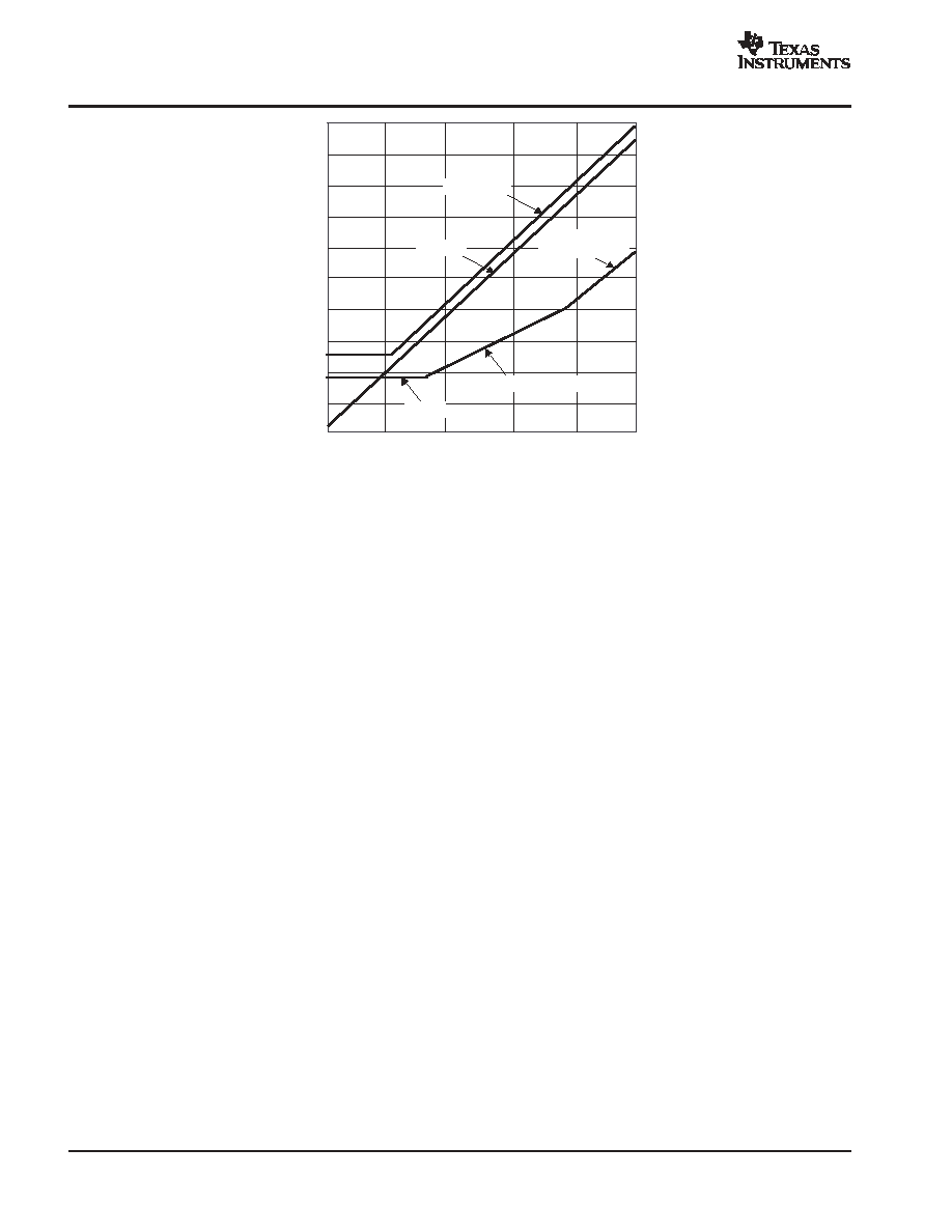
ZVCHG pin behavior is shown in Figure 9 where V
(ZVCHG)
is set to 0 V at the beginning.
bq29312
SLUS546D - MARCH 2003 - REVISED SEPTEMBER 2004
www.ti.com
24
t - Time - mS
V
oltage - V
0
4
8
12
16
4
20
10
0
8
2
6
14
18
12
16
20
V(PACK)
3.5 V
V(ZVCHG)=
V(PACK) - 8 V
V(ZVCHG)= V(PACK) / 2
V(BAT)
Figure 9. Voltage Transition at ZVCHG, PACK and BAT
As V
(PACK)
exceeds 7 V, V
(ZVCHG)
= V
(PACK)
/2. However, V
(ZVCHG)
is maintained to limit the voltage between PACK and
ZVCHG at a maximum of 8 V(typ). This limitation is intended to avoid excessive voltage between the gate and the source
of ZVCHG-FET.
The signal timing is shown in Figure 10. When precharge begins (V
(BAT)
= 0 V) V
(PACK)
is clamped to 3.5 V and holds the
supply voltage for bq29312 operation. After V
(BAT)
reaches sufficient voltage high enough for bq29312 operation, the
CHG-FET and the DSG-FET are turned ON and ZVCHG-FET is turned OFF.
Although the current path is changed, the same precharging current is still applied. When V
(BAT)
reaches the fast charging
voltage (typical 3 V per cell), the charger switches into fast charging mode.
bq29312
SLUS546D - MARCH 2003 - REVISED SEPTEMBER 2004
www.ti.com
25
ON
ZVCHG FET = OFF
OFF
CHG FET = ON
OFF
CHG FET = ON
3.5 V+VGS(ZVCHGFET)
0 V
3.3 V
0 V
V = VPACK*(1/2)
3.5 V (typ.)
0 V
"L" (1 V)
"L" (1 V)
0 V
Fast Charge Current
0 V and Precharge Current
0 A
0 V Charge
Mode
Precharge
Mode
Fast Charge Mode
V(PACK)
REG
ZVCHG
GHD
DSG
Battery
Voltage
Charge
Current
Figure 10. Signal Timing of Pins During 0 V Charging and Precharging (0 V Charge FET)
Common FET
This mode does not require a dedicated precharge FET (ZVCHG-FET). The charge FET (CHG-FET) is ON at initialization
of the bq29312 when PMS = V
(PACK)
allowing for 0 V or precharge current to flow. The application circuit is shown in Figure
11. The charger is expected to provide the precharge function in this mode, where the charger provides a precharge current
level suitable to charge cells below a set level, typically below 3.0 V per cell. When the lowest cell voltage rises above this
level then a fast charging current is applied.
When the charger is connected the voltage at PMS rises. Once it is above 0.7 V, the CHG output is driven to GND which
turns ON the CHG-FET. The charging current flows through the CHG-FET and a back diode of DSG-FET. The pack voltage
is represented by the following equation.
V
(PACK)
= V
(BAT)
+ V
F
+
V
DS(CHG-FET)
Where V
F
= 0.7 V is the forward voltage of a DSG-FET back diode and is typically 0.7 V.
While V
(PACK)
is maintained above 0.7 V the precharging current is maintained. While V
(PACK)
and V
(BAT)
are under the
bq29312 supply voltage then the bq29312 regulator is inactive and the host controller is not functional. Thus, any protection
features of this chipset do not function during this period. This state continues until V
(PACK)
goes higher than the bq29312
minimum supply voltage.
When V
(BAT)
rises and V
(PACK)
reaches bq29312 minimum supply voltage, the REG output is active providing a 3.3 V (typ)
supply to the host. When this level is reached the CHG pin changes its state from GND to the level controlled with CHG
bit in bq29312 registers. In this state, the CHG output level is driven by a clamp circuit so that its voltage level changes
from 0 V to 1 V. Also, the host controller is active and can turn ON the DSG-FET.
The disadvantages is that during 0 V charging, bq29312 is inactive. The device does not protect the battery and does not
update battery information (now is 0 V charging) to the PC.
bq29312
SLUS546D - MARCH 2003 - REVISED SEPTEMBER 2004
www.ti.com
26
There are two advantage of this configuration:
1.
The voltage between BAT and PACK is lower. Higher precharge current is allowed due to less heat loss is the
FET and no external resistor required.
2.
The charge FET is turned on during precharging. The precharge current can be fully controlled by the charger.
PACK
ZVCHG
PMS
REG
CHG
DSG
BAT
4.7
µ
F
Battery
DSG-FET
CHG-FET
Pack+
I(ZVCHG)
I(FASTCHG)
CV
CC
Charger
DC Input
bq29312
I(ZVCHG) = 0 V Percharge Current
I(FASTCHG) = Fast Current
OD
NC
Figure 11. Common FET Mode Circuit Diagram
The signal timing during the common FET mode is shown in Figure 12. The CHG-FET is turned on when the charger is
connected. As V
(BAT)
rises and V
(PACK)
reaches the bq29312 minimum supply voltage, the REG output becomes active
and the host controller starts to work.
When V
(PACK)
becomes high enough, the host controller turns ON the DSG-FET. The charger enters the fast charging mode
when V
(BAT)
reaches the fast charge level.

bq29312
SLUS546D - MARCH 2003 - REVISED SEPTEMBER 2004
www.ti.com
27
0 V Precharge Mode
Fast Charge Mode
V(PACK)
REG
PMS
CHG
DSG
Battery
Voltage
Charge
Current
Host =
Inactive
Host = Active
Set to "L" as
PMS = PACK
Set to "L" by Host
Host Sets
DSG-FET to ON
0.7 V
0 V
3.3 V
0 V
0 V
"L" (1 V)
0 V
"L" (1 V)
0 V
Fast Charge Current
0 V and Precharge Current
0 A
Figure 12. Signal Timing of Pins During 0 V Charging and Precharging (Common FET)
Precharge FET
This mode has a dedicated precharge current path using an additional open drain driven FET (PCHG-FET) and sustains
the
V
(PACK)
level. In this mode, where the PMS input is connected to GND, the bq29312 and host combine to provide the
precharge function by limiting the fast charge current which is provided by the system side charger.
Figure 13 shows the bq29312 application circuit in this mode.
PACK
ZVCHG
PMS
REG
CHG
DSG
BAT
PCHG-FET
R(PCHG)
4.7
µ
F
Battery
DSG-FET
CHG-FET
Pack+
I(FASTCHG)
CV
CC
Charger
DC Input
bq29312
I(FASTCHG) = Fast Current
OD
Host
SCLK SDATA
Figure 13. Precharge FET Mode Circuit Diagram

bq29312
SLUS546D - MARCH 2003 - REVISED SEPTEMBER 2004
www.ti.com
28
The PCHG-FET is driven by the OD output and the resister R
(PCHG)
in the precharge path limits the precharge current.
When OD = GND then the PCHG-FET is ON. The precharge current is represented by the following equation:
I
(PCHG)
= ID = ( V
(PACK)
V
(BAT)
V
DS
)/R
(PCHG)
A load curve of the PCHG-FET is shown in Figure 13. When the drain-source voltage (V
DS
) is high enough, the PCHG-FET
operates in the linear region and has low resistance. By approximating V
DS
as 0 V, the precharge current, I
(PCHG)
is
expressed as below.
I
(PCHG)
= ( V
(PACK)
V
(BAT)
)/R
(PCHG)
ID
VSD
ID = (V(PACK) - V(BAT) - VDS)/R(PCHG)
Figure 14. PCHG-FET ID--VDS Characteristic
During the precharge phase, CHG-FET is turned OFF and PCHG-FET is turned ON. When all the cell voltages measured
by the host reach the fast charge threshold, the host controller turns ON CHG-FET and turns OFF PCHG-FET. The signal
timing is shown in Figure 15.
When the charger is connected, CHG-FET, DSG-FET and PCHG-FET are already in the OFF state. When the charger in
connected it applies V
(PACK)
. The bq29312 REG output then becomes active and supplies power to the host controller. As
the host controller starts up, it turns on the OD pin and the precharge current is enabled.
In this configuration, attention must be paid to high power consumption in the PCHG-FET and the series resistor R
(PCHG)
.
The highest power is consumed when V
BAT
= 0 V, where it is the highest differential between the PACK and BAT pins. For
example, the power consumption in 4 series cells with 17.4 V fast charge voltage and R
(PCHG)
=
188
is expressed below.
I
PCHG
= (17.4 V 0.0 V)/188
= 92.6 mA
17.4 V x 92.6 mA = 1.61 W
An optional solution is to combine a thermistor with a resistor to create R
(PCHG)
, therefore, as temperature increases, the
current reduces.
Once the lowest cell voltage reaches the fast charge level (typ 3.0v per cell), the host controller turns ON CHG-FET and
DSG-FET, and turns OFF PCHG-FET.
It is also appropriate to turn on DSG-FET during precharge in order to supply precharge current efficiently, as shown in
Figure 15.

bq29312
SLUS546D - MARCH 2003 - REVISED SEPTEMBER 2004
www.ti.com
29
Charge CV
0 V
Host : Active
3.3 V
0 V
OFF
CHG FET = OFF
OFF
0 V
DSG FET = ON
"L" (1 V)
OFF
"L" (1 V)
0 V
Fast Charge Current
0 V and Precharge Current
0 A
0 V and
Precharge Mode
Fast Charge
Mode
V(PACK)
REG
CHG
DSG
Battery
Voltage
Charge
Current
Charge
Charge Mode
OD
PCHG FET = ON
Figure 15. Signal Timing of Pins During 0 V Charging and Precharging (Precharge FET)
Summary
The three types of 0-V charge options available with the bq29312 are summarized below:
CHARGE OPTIONS
CHARGE MODE TYPE
HOST CHARGE CAPABILITIES
KEY APPLICATION CIRCUIT NOTES
CHARGE MODE TYPE
HOST CHARGE CAPABILITIES
KEY APPLICATION CIRCUIT NOTES
1) 0-V Charge FET
Fast charge and precharge
PMS = GND
ZVCHG: Drives 0-V charge FET
(ZVCHG-FET)
OD: Not used
2) Common FET
Fast charge and precharge
PMS = PACK
ZVCHG: Not used
OD: Not used
3) Precharge FET
Fast charge but no precharge function
PMS = GND
ZVCHG: Not used
OD: Drives the precharge FET
(PCHG-FET)

bq29312
SLUS546D - MARCH 2003 - REVISED SEPTEMBER 2004
www.ti.com
30
There a number of tradeoffs between the various 0-V charge modes which are discussed below.
D
0-V Charge FET (1) vs Common FET (2)
When the charger has both of precharge and charging functions, there are two types of circuit configuration available.
1.
0-V Charge FET - The bq29312 is active even during precharge. Therefore, the host can update the battery
status to the system and protect the battery pack by detecting abnormal conditions.
- A high voltage is applied on the 0-V charge FET at 0-V cell voltage. In order to avoid excessive heat generation
the 0-V charge current must be limited.
2.
Common FET - During 0-V charge the bq29312 and the host are not active. Therefore, they cannot protect the
cells and cannot update the battery status to the system.
- The bq29312 can tolerate high 0-V charge current as heat generation is not excessive.
- A dedicated FET for the 0-V charge is not required.
D
0-V Charge FET (1) vs Precharge FET (3)
The current paths of the 0-V charge FET (1) and Precharge FET (3) modes are the same. If the 0-V charge FET (1) mode
is used with chargers without precharge function, the bq29312 consumes extra current of up to 1 mA in order to turn ON
the ZVCHG output.
1.
If the charger has a precharge function - ZVCHG-FET is turned ON only during 0-V charging. In this case, 1 mA
increase is not a concern because the charger is connected during the 0-V charging period.
2.
If the charger does not have precharge function - The ZVCHG-FET must be turned ON during 0-V charging and
also precharging. When the battery reaches an over discharged state, it must turn OFF DSG-FET and CHG-FET
and turn ON ZVCHG-FET. The reason for this is the battery must keep the 0-V charge path while waiting for a
charger to be connected to limit the current.
- Consuming 1 mA, while waiting for a charger to be connected in over discharge state, is significant if compared
to current consumption of other modes.
D
Precharge FET (3)
If the precharge FET (3) mode is used with a charger with precharge function, care must be taken as limiting the 0-V charge
current with resistance may cause some issues. The charger may start fast charge immediately, or detect an abnormal
condition.
When the charger is connected, the charger may raise the output voltage to force the precharge current. In order to assure
a supply voltage for the bq29312 during 0-V charging, the resistance of a series resister (R
PCHG
) must be high enough.
This may result in a very high V
PACK
, and some chargers may detect it as an abnormal condition.
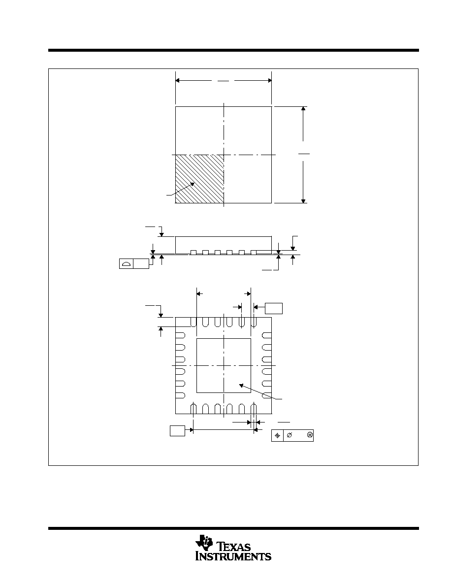
MECHANICAL DATA
MPQF124A FEBRUARY 2002 REVISED DECEMBER 2002
1
POST OFFICE BOX 655303
·
DALLAS, TEXAS 75265
RGE (S-PQFP-N24)
PLASTIC QUAD FLATPACK
Seating Plane
4204104/B 11/02
1,00
0,80
0,18
0,30
0,05
Exposed Thermal Die Pad
(See Note D)
Pin 1 Index Area
Top and Bottom
0,00
1
6
4,15
0,50
0,30
3,85
0,08
0,10
3,85
4,15
2,55 MAX SQ.
24
18
13
19
12
7
24X
2,50
24X
0,50
0,20 REF.
NOTES: A. All linear dimensions are in millimeters.
B. This drawing is subject to change without notice.
C. Quad Flatpack, No-leads, (QFN) package configuration.
D. The package thermal performance may be enhanced by bonding the thermal die pad to an external thermal plane.
E. Falls within JEDEC M0-220.
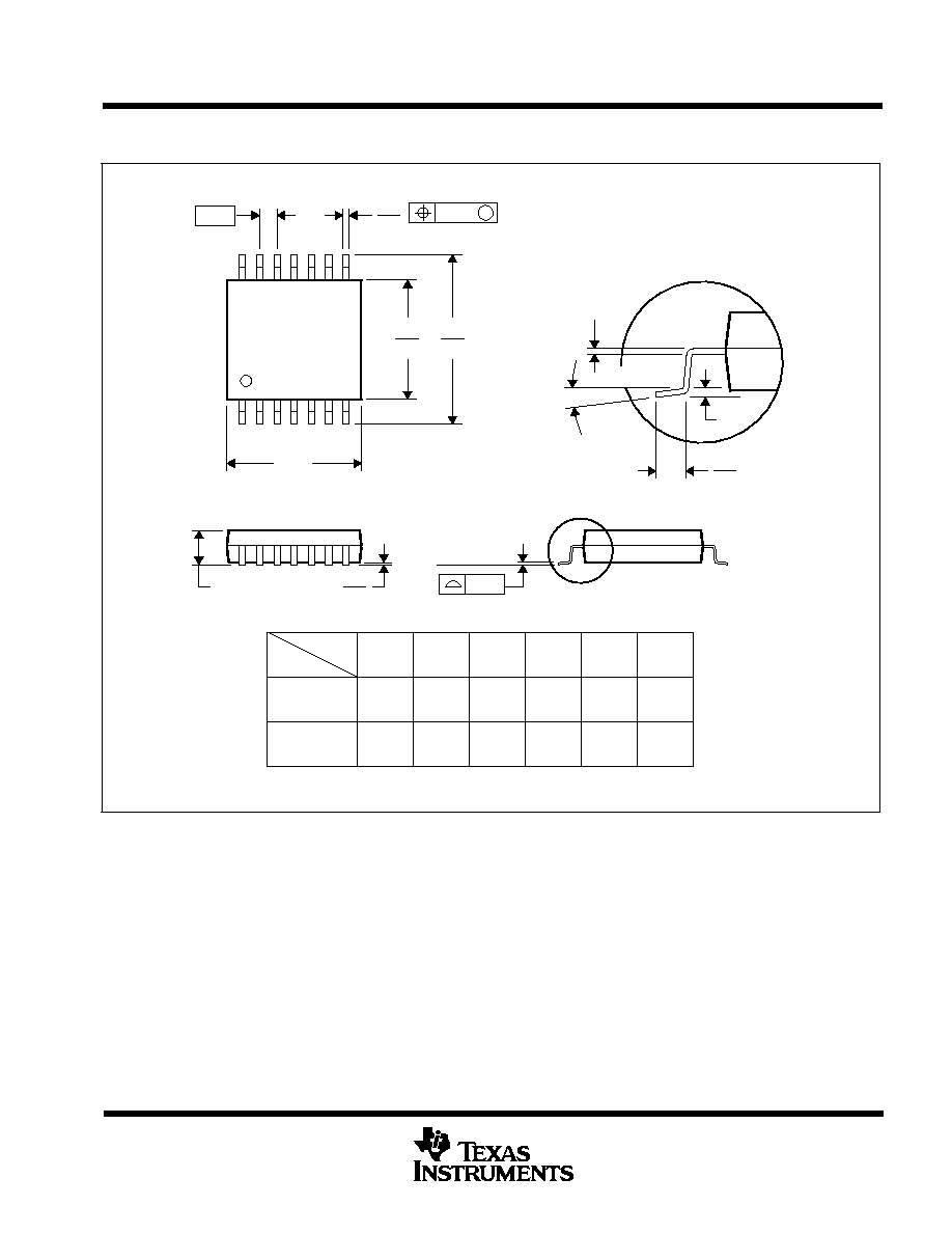
MECHANICAL DATA
MTSS001C JANUARY 1995 REVISED FEBRUARY 1999
POST OFFICE BOX 655303
·
DALLAS, TEXAS 75265
PW (R-PDSO-G**)
PLASTIC SMALL-OUTLINE PACKAGE
14 PINS SHOWN
0,65
M
0,10
0,10
0,25
0,50
0,75
0,15 NOM
Gage Plane
28
9,80
9,60
24
7,90
7,70
20
16
6,60
6,40
4040064/F 01/97
0,30
6,60
6,20
8
0,19
4,30
4,50
7
0,15
14
A
1
1,20 MAX
14
5,10
4,90
8
3,10
2,90
A MAX
A MIN
DIM
PINS **
0,05
4,90
5,10
Seating Plane
0
°
8
°
NOTES: A. All linear dimensions are in millimeters.
B. This drawing is subject to change without notice.
C. Body dimensions do not include mold flash or protrusion not to exceed 0,15.
D. Falls within JEDEC MO-153

IMPORTANT NOTICE
Texas Instruments Incorporated and its subsidiaries (TI) reserve the right to make corrections, modifications,
enhancements, improvements, and other changes to its products and services at any time and to discontinue
any product or service without notice. Customers should obtain the latest relevant information before placing
orders and should verify that such information is current and complete. All products are sold subject to TI's terms
and conditions of sale supplied at the time of order acknowledgment.
TI warrants performance of its hardware products to the specifications applicable at the time of sale in
accordance with TI's standard warranty. Testing and other quality control techniques are used to the extent TI
deems necessary to support this warranty. Except where mandated by government requirements, testing of all
parameters of each product is not necessarily performed.
TI assumes no liability for applications assistance or customer product design. Customers are responsible for
their products and applications using TI components. To minimize the risks associated with customer products
and applications, customers should provide adequate design and operating safeguards.
TI does not warrant or represent that any license, either express or implied, is granted under any TI patent right,
copyright, mask work right, or other TI intellectual property right relating to any combination, machine, or process
in which TI products or services are used. Information published by TI regarding third-party products or services
does not constitute a license from TI to use such products or services or a warranty or endorsement thereof.
Use of such information may require a license from a third party under the patents or other intellectual property
of the third party, or a license from TI under the patents or other intellectual property of TI.
Reproduction of information in TI data books or data sheets is permissible only if reproduction is without
alteration and is accompanied by all associated warranties, conditions, limitations, and notices. Reproduction
of this information with alteration is an unfair and deceptive business practice. TI is not responsible or liable for
such altered documentation.
Resale of TI products or services with statements different from or beyond the parameters stated by TI for that
product or service voids all express and any implied warranties for the associated TI product or service and
is an unfair and deceptive business practice. TI is not responsible or liable for any such statements.
Following are URLs where you can obtain information on other Texas Instruments products and application
solutions:
Products
Applications
Amplifiers
amplifier.ti.com
Audio
www.ti.com/audio
Data Converters
dataconverter.ti.com
Automotive
www.ti.com/automotive
DSP
dsp.ti.com
Broadband
www.ti.com/broadband
Interface
interface.ti.com
Digital Control
www.ti.com/digitalcontrol
Logic
logic.ti.com
Military
www.ti.com/military
Power Mgmt
power.ti.com
Optical Networking
www.ti.com/opticalnetwork
Microcontrollers
microcontroller.ti.com
Security
www.ti.com/security
Telephony
www.ti.com/telephony
Video & Imaging
www.ti.com/video
Wireless
www.ti.com/wireless
Mailing Address:
Texas Instruments
Post Office Box 655303 Dallas, Texas 75265
Copyright
2004, Texas Instruments Incorporated