ADS900: SpeedPlus 10-Bit, 20MHz, +3V Supply Analog-To-Digital Converter (Rev. A )
FEATURES
q
+2.7V TO +3.7V SUPPLY OPERATION
q
INTERNAL REFERENCE
q
LOW POWER: 52mW at +3V
q
SINGLE-ENDED INPUT RANGE: 1V to 2V
q
WIDEBAND TRACK/HOLD: 350MHz
q
SSOP-28 PACKAGE
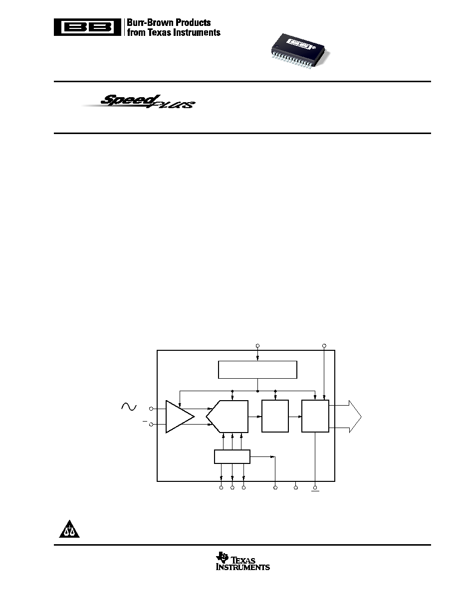
DESCRIPTION
The ADS900 is a high-speed pipelined Analog-to-Digital
Converter (ADC). This complete converter includes a high
bandwidth track-and-hold, a 10-bit quantizer, and an inter-
nal reference.
The ADS900 employs digital error correction techniques to
provide excellent differential linearity for demanding im-
aging applications. Its low distortion and high SNR give the
extra margin needed for telecommunications, video and
test instrumentation applications.
This high-performance ADC is specified for performance
at a 20MHz sampling rate. The ADS900 is available in an
SSOP-28 package.
10-Bit, 20MHz, +3V Supply
ANALOG-TO-DIGITAL CONVERTER
APPLICATIONS
q
PORTABLE INSTRUMENTATION
q
IF AND BASEBAND COMMUNICATIONS
q
CABLE MODEMS
q
SET-TOP BOXES
q
PORTABLE TEST EQUIPMENT
q
COMPUTER SCANNERS
TM
Pipeline
A/D
Internal
Reference
Timing
Circuitry
Error
Correction
3-State
Outputs
T/H
10-Bit
Digital
Data
CLK
ADS900
LV
DD
OE
Pwrdn
1V
REF
LnBy
CM
LpBy
IN
2V
1V
IN
(Opt.)
ADS900
SBAS058A MAY 2001
www.ti.com
PRODUCTION DATA information is current as of publication date.
Products conform to specifications per the terms of Texas Instruments
standard warranty. Production processing does not necessarily include
testing of all parameters.
Copyright © 1997, Texas Instruments Incorporated
Please be aware that an important notice concerning availability, standard warranty, and use in critical applications of
Texas Instruments semiconductor products and disclaimers thereto appears at the end of this data sheet.
ADS9
00E
ADS900
2
SBAS058A
ELECTRICAL CHARACTERISTICS
At T
A
= +25
°
C, V
S
= LV
DD
= +3V, Single-Ended Input, Sampling Rate = 20MHz, unless otherwise specified.
ELECTROSTATIC
DISCHARGE SENSITIVITY
This integrated circuit can be damaged by ESD. Texas Instru-
ments recommends that all integrated circuits be handled with
appropriate precautions. Failure to observe proper handling
and installation procedures can cause damage.
ESD damage can range from subtle performance degradation
to complete device failure. Precision integrated circuits may
be more susceptible to damage because very small parametric
changes could cause the device not to meet its published
specifications.
+V
S
....................................................................................................... +6V
Analog Input ............................................................................... +V
S
+0.3V
Logic Input ................................................................................. +V
S
+0.3V
Case Temperature ......................................................................... +100
°
C
Junction Temperature .................................................................... +150
°
C
Storage Temperature ..................................................................... +150
°
C
ABSOLUTE MAXIMUM RATINGS
ADS900E
PARAMETER
CONDITIONS
TEMP
MIN
TYP
MAX
UNITS
Resolution
10
Bits
Specified Temperature Range
Ambient Air
40
+85
°
C
ANALOG INPUT
Single-Ended Full Scale Input Range
(1Vp-p)
+1.0
+2.0
V
Differential Full Scale Input Range
(0.5Vp-pX 2)
+1.25
+1.75
V
Common-Mode Voltage
1.5
V
Analog Input Bias Current
1
µ
A
Input Impedance
1.25 || 5
M
|| pF
DIGITAL INPUTS
Logic Family
TTL/HCT COMPATIBLE CMOS
High Input Voltage, V
IH
2.0
V
DD
V
Low Input Voltage, V
IL
0.8
V
High Input Current, I
IH
±
10
µ
A
Low Input Current, I
IL
±
10
µ
A
Input Capacitance
5
pF
CONVERSION CHARACTERISTICS
Start Conversion
RISING EDGE OF CONVERT CLOCK
Sample Rate
Full
10k
20M
Samples/s
Data Latency
5
Clk Cyc
PACKAGE
SPECIFIED
DRAWING
TEMPERATURE
PACKAGE
ORDERING
TRANSPORT
PRODUCT
PACKAGE
NUMBER
RANGE
MARKING
NUMBER
(1)
MEDIA
ADS900E
SSOP-28
324
40
°
C to +85
°
C
ADS900E
ADS900E
Rails
"
"
"
"
ADS900E
ADS900E/1K
Tape and Reel
NOTE: (1) Models with a slash (/) are available only in Tape and Reel in the quantities indicated (e.g., /1K indicates 1000 devices per reel). Ordering 1000 pieces
of "ADS900E/1K" will get a single 1000-piece Tape and Reel.
PACKAGE/ORDERING INFORMATION
ADS900
3
SBAS058A
ELECTRICAL CHARACTERISTICS
(Cont.)
At T
A
= +25
°
C, V
S
= +3V, Single-Ended Input, Sampling Rate = 20MHz, unless otherwise specified.
ADS900E
PARAMETER
CONDITIONS
TEMP
MIN
TYP
MAX
UNITS
DYNAMIC CHARACTERISTICS
Differential Linearity Error
f = 500kHz
(Largest Code Error)
Full
±
0.7
LSBs
f = 10MHz
(Largest Code Error)
Full
±
0.7
±
1.0
LSBs
No Missing Codes
Full
Guaranteed
Integral Nonlinearity Error, f = 500kHz
Full
±
3.5
LSBs
Spurious Free Dynamic Range
(1)
f = 500kHz (1dBFS
(2)
input)
Full
53
dBFS
(2)
f = 10MHz (1dBFS
(2)
input)
Full
47
53
dBFS
Two-Tone Intermodulation Distortion
(3)
f = 4.5MHz and 5.0MHz (7dBFS each tone)
+25
°
C
50
dBc
Signal-to-Noise Ratio (SNR)
f = 500kHz (1dBFS input)
Full
49
dB
f = 10MHz (1dBFS input)
Full
45
49
dB
Signal-to-(Noise + Distortion) (SINAD)
f = 500kHz (1dBFS input)
Full
48
dB
f = 3.58MHz (1dBFS input)
Full
48
dB
f = 10MHz (1dBFS input)
Full
44
48
dB
Differential Gain Error
NTSC, PAL
2.3
%
Differential Phase Error
NTSC, PAL
1
degrees
Output Noise
Input Grounded
0.2
LSBs rms
Aperture Delay Time
2
ns
Aperture Jitter
7
ps rms
Analog Input Bandwidth
Small Signal
20dBFS Input
+25
°
C
350
MHz
Full Power
0dBFS Input
+25
°
C
100
MHz
Overvoltage Recovery Time
(4)
1.5X FS Input
+25
°
C
2
ns
DIGITAL OUTPUTS
C
L
= 15pF
Logic Family
TTL/HCT COMPATIBLE CMOS
Logic Coding
Straight Offset Binary
High Output Voltage, V
OH
+2.4
LV
DD
V
Low Output Voltage, V
OL
+0.4
V
3-State Enable Time
OE = L
20
40
ns
3-State Disable Time
OE = H
2
10
ns
Internal Pull-Down
50
k
Power-Down Enable Time
PwrDn = L
133
ns
Power-Down Disable Time
PwrDn = H
18
ns
Internal Pull-Down
50
k
ACCURACY
f
S
= 2.5MHz
Gain Error
+25
°
C
8
±
10
%FS
Input Offset
Referred to Ideal Midscale
Full
15
±
60
mV
Power Supply Rejection (Gain)
V
S
= +10%
Full
55
dB
Power Supply Rejection (Offset)
Full
62
dB
Internal Positive Reference Voltage
Full
+1.75
V
Internal Negative Reference Voltage
Full
+1.25
V
POWER SUPPLY REQUIREMENTS
Supply Voltage: +V
S
Operating
Full
+2.7
+3
+3.7
V
Supply Current: +I
S
Operating
Full
18
22
mA
Power Dissipation
Operating, +3V
Full
54
66
mW
25
°
C
52
mW
Power Dissipation (Power Down)
+3V
Full
10
mW
Thermal Resistance,
JA
SSOP-28
89
°
C/W
NOTES: (1) Spurious Free Dynamic Range refers to the magnitude of the largest harmonic. (2) dBFS means dB relative to full scale. (3) Two-tone intermodulation
distortion is referred to the largest fundamental tone. This number will be 6dB higher if it is referred to the magnitude of the two-tone fundamental envelope. (4) No
rollover of bits.
ADS900
4
SBAS058A
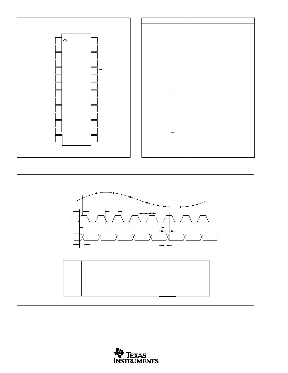
5 Clock Cycles
Data Invalid
t
D
t
L
t
H
t
CONV
N5
N4
N3
N2
N1
N
N+1
N+2
Data Out
Clock
Analog In
N
t
2
N+1
N+2
N+3
N+4
N+5
N+6
N+7
t
1
PIN CONFIGURATION
PIN
DESIGNATOR
DESCRIPTION
1
+V
S
Analog Supply
2
LV
DD
Output Logic Driver Supply Voltage
3
Bit 10
Data Bit 10 (D0) (LSB)
4
Bit 9
Data Bit 9 (D1)
5
Bit 8
Data Bit 8 (D2)
6
Bit 7
Data Bit 7 (D3)
7
Bit 6
Data Bit 6 (D4)
8
Bit 5
Data Bit 5 (D5)
9
Bit 4
Data Bit 4 (D6)
10
Bit 3
Data Bit 3 (D7)
11
Bit 2
Data Bit 2 (D8)
12
Bit 1
Data Bit 1 (D9) (MSB)
13
GND
Analog Ground
14
GND
Analog Ground
15
CLK
Convert Clock Input
16
OE
Output Enable, Active Low
17
Pwrdn
Power Down Pin
18
+V
S
Analog Supply
19
GND
Analog Ground
20
GND
Analog Ground
21
LpBy
Positive Ladder Bypass
22
NC
No Connection
23
1V
REF
1V Reference Output
24
IN
Complementary Input
25
LnBy
Negative Ladder Bypass
26
CM
Common-Mode Voltage Output
27
IN
Analog Input
28
+V
S
Analog Supply
PIN DESCRIPTIONS
Top View
SSOP
TIMING DIAGRAM
SYMBOL
DESCRIPTION
MIN
TYP
MAX
UNITS
t
CONV
Convert Clock Period
50
100
µ
s
ns
t
L
Clock Pulse Low
24
25
ns
t
H
Clock Pulse High
24
25
ns
t
D
Aperture Delay
2
ns
t
1
Data Hold Time, C
L
= 0pF
3.9
ns
t
2
New Data Delay Time, C
L
= 15pF max
12
ns
+V
S
LV
DD
LSB Bit 10
Bit 9
Bit 8
Bit 7
Bit 6
Bit 5
Bit 4
Bit 3
Bit 2
MSB Bit 1
GND
GND
+V
S
IN
CM
LnBy
IN
1V
REF
NC
LpBy
GND
GND
+V
S
Pwrdn
OE
CLK
1
2
3
4
5
6
7
8
9
10
11
12
13
14
28
27
26
25
24
23
22
21
20
19
18
17
16
15
ADS900
ADS900
5
SBAS058A
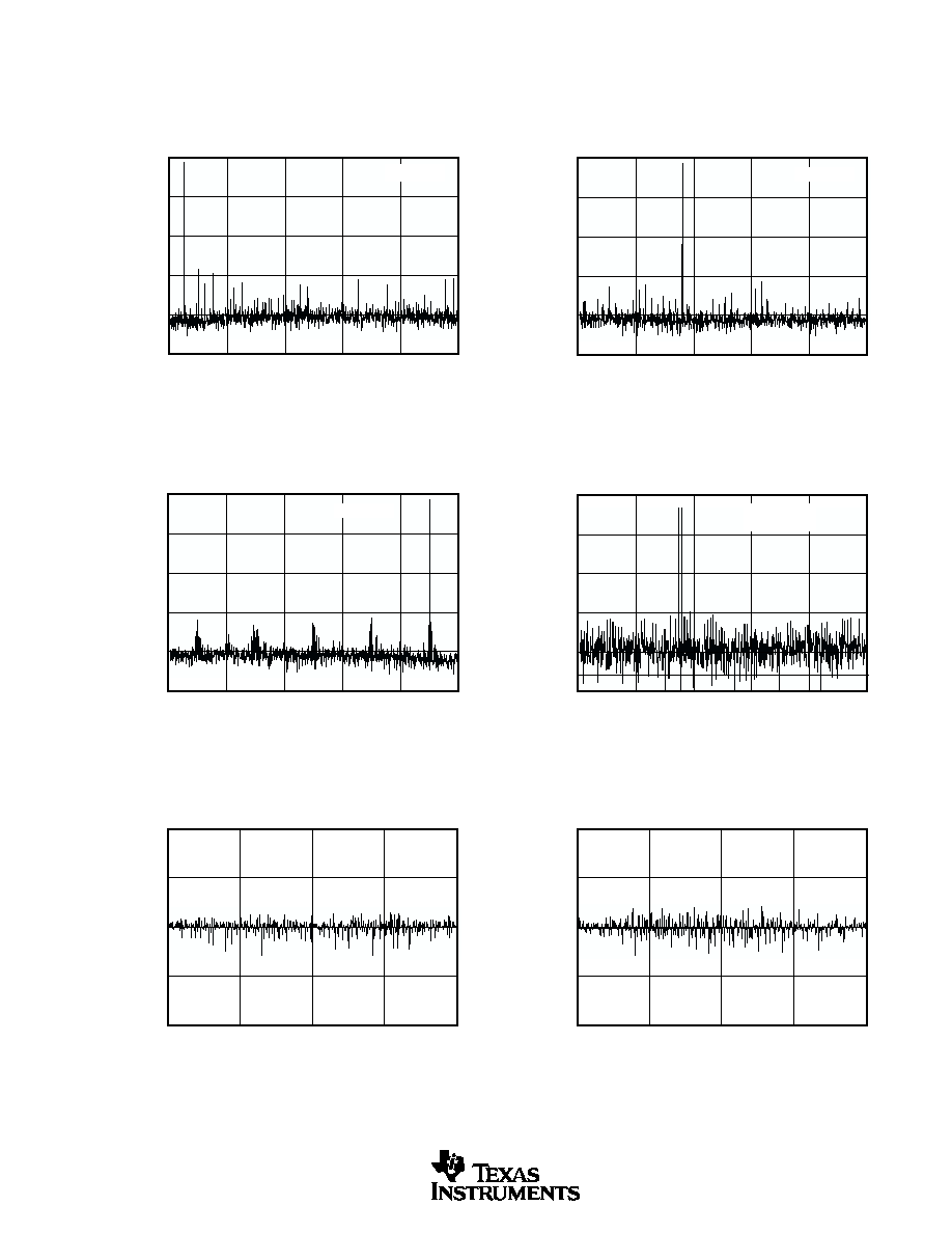
TWO-TONE INTERMODULATION
Frequency (MHz)
0
20
40
60
80
100
0
2
4
8
6
10
Magnitude (dBFS)
f
1
= 3.5MHz at 7dBFS
f
2
= 3.4MHz at 7dBFS
SPECTRAL PERFORMANCE
Frequency (MHz)
0
20
40
60
80
100
0
2
4
6
8
10
Amplitude (dB)
f
IN
= 9MHz
SPECTRAL PERFORMANCE
Frequency (MHz)
0
20
40
60
80
100
0
2
4
6
8
10
Amplitude (dB)
f
IN
= 3MHz
SPECTRAL PERFORMANCE
Frequency (MHz)
0
20
40
60
80
100
0
2
4
6
8
10
Amplitude (dB)
f
IN
= 500kHz
0
256
512
768
1024
DIFFERENTIAL LINEARITY ERROR
Output Code
2.0
1.0
0.0
1.0
2.0
Error (LSB)
f
IN
= 10MHz
DIFFERENTIAL LINEARITY ERROR
Output Code
2.0
1.0
0.0
1.0
2.0
0
256
512
768
1024
DLE (LSB)
f
IN
= 500kHz
TYPICAL CHARACTERISTICS
At T
A
= +25
°
C, V
S
= LV
DD
= +3V, Single-Ended Input, Sampling Rate = 20MHz, unless otherwise specified.