
Dual, 500kHz, 12-Bit, 2 + 2 Channel,
Simultaneous Sampling
ANALOG-TO-DIGITAL CONVERTER
FEATURES
q
4 INPUT CHANNELS
q
FULLY DIFFERENTIAL INPUTS
q
2
Á
s TOTAL THROUGHPUT PER CHANNEL
q
GUARANTEED NO MISSING CODES
q
1MHz EFFECTIVE SAMPLING RATE
q
LOW POWER: 40mW
q
SSI SERIAL INTERFACE
APPLICATIONS
q
MOTOR CONTROL
q
MULTI-AXIS POSITIONING SYSTEMS
q
3-PHASE POWER CONTROL
DESCRIPTION
The ADS7861 is a dual, 12-bit, 500kHz, Analog-to-Digital
(A/D) converter with 4 fully differential input channels grouped
into two pairs for high speed, simultaneous signal acquisition.
Inputs to the sample-and-hold amplifiers are fully differential
and are maintained differential to the input of the A/D con-
verter. This provides excellent common-mode rejection of
80dB at 50kHz which is important in high noise environments.
The ADS7861 offers a high-speed, dual serial interface and
control inputs to minimize software overhead. The output data
for each channel is available as a 12-bit word. The ADS7861
is offered in an SSOP-24 package and is fully specified over
the ş40
░
C to +85
░
C operating range.
ADS7
861
SAR
Serial
Interface
COMP
CLOCK
A0
M1
M0
CONVST
CS
RD
BUSY
SERIAL DATA B
SERIAL DATA A
CDAC
Internal
2.5V
Reference
SHA
CH A0ş
CH A0+
REF
IN
CH A1ş
CH A1+
SAR
COMP
CDAC
SHA
CH B0ş
CH B0+
CH B1ş
CH B1+
REF
OUT
ADS7861
SBAS110A ş MAY 2001
www.ti.com
PRODUCTION DATA information is current as of publication date.
Products conform to specifications per the terms of Texas Instruments
standard warranty. Production processing does not necessarily include
testing of all parameters.
Copyright ę 1998, Texas Instruments Incorporated
Please be aware that an important notice concerning availability, standard warranty, and use in critical applications of
Texas Instruments semiconductor products and disclaimers thereto appears at the end of this data sheet.

ADS7861
2
SBAS110A
ABSOLUTE MAXIMUM RATINGS
Analog Inputs to AGND, Any Channel Input ........ ş0.3V to (+V
D
+ 0.3V)
REF
IN
..................................................................... ş0.3V to (+V
D
+ 0.3V)
Digital Inputs to DGND .......................................... ş0.3V to (+V
D
+ 0.3V)
Ground Voltage Differences: AGND, DGND ...................................
▒
0.3V
+V
D
to AGND ......................... ş0.3V to +6V
Power Dissipation .......................................................................... 325mW
Maximum Junction Temperature ................................................... +150
░
C
Operating Temperature Range ........................................ ş40
░
C to +85
░
C
Storage Temperature Range ......................................... ş65
░
C to +150
░
C
Lead Temperature (soldering, 10s) ............................................... +300
░
C
ELECTROSTATIC
DISCHARGE SENSITIVITY
This integrated circuit can be damaged by ESD. Texas Instru-
ments recommends that all integrated circuits be handled with
appropriate precautions. Failure to observe proper handling and
installation procedures can cause damage.
ESD damage can range from subtle performance degradation to
complete device failure. Precision integrated circuits may be
more susceptible to damage because very small parametric
changes could cause the device not to meet its published specifi-
cations.
MINIMUM
RELATIVE
MAXIMUM
SPECIFICATION
PACKAGE
ACCURACY
GAIN ERROR
TEMPERATURE
DRAWING
ORDERING
TRANSPORT
PRODUCT
(LSB)
(%)
RANGE
PACKAGE
NUMBER
NUMBER
(1)
MEDIA
ADS7861E
▒
2
▒
0.75
ş40
░
C to +85
░
C
SSOP-24
352
ADS7861E
Rails
"
"
"
"
"
"
ADS7861EB/2K5
Tape and Reel
ADS7861EB
▒
1
▒
0.5
ş40
░
C to +85
░
C
SSOP-24
352
ADS7861E
Rails
"
"
"
"
"
"
ADS7861EB/2K5
Tape and Reel
NOTE: (1) Models with a slash (/) are available only in Tape and Reel in the quantities indicated (e.g., /2K indicates 2000 devices per reel). Ordering 2000 pieces
of "ADS7861E/2K" will get a single 2000-piece Tape and Reel.
PACKAGE/ORDERING INFORMATION
BASIC CIRCUIT CONFIGURATION
M0
M1
A0
TWO-CHANNEL/FOUR-CHANNEL OPERATION
DATA ON SERIAL OUTPUTS
CHANNELS CONVERTED
0
0
0
Two Channel
A and B
A0, B0
0
0
1
Two Channel
A and B
A1, B1
0
1
0
Two Channel
A Only
A0, B0
0
1
1
Two Channel
A Only
A1, B1
1
0
X
Four Channel
A and B
Sequential
1
1
X
Four Channel
A Only
Sequential
X = Don't Care.
TRUTH TABLE
DGND
CH B1+
CH B1ş
CH B0+
CH B0ş
CH A1+
CH A1ş
CH A0+
CH A0ş
REF
IN
REF
OUT
AGND
1
2
3
4
5
6
7
8
9
10
11
12
24
23
22
21
20
19
18
17
16
15
14
13
+V
D
SERIAL DATA A
SERIAL DATA B
BUSY
CLOCK
CS
RD
CONVST
A0
M0
M1
+V
A
BUSY Output
Clock Input
Chip Select
Read Input
Conversion Start
A0 Address Select
M0 Address Select
M1 Address Select
ADS7861
10
Á
F
+
0.1
Á
F
+5V Analog Supply
+
ADS7861
3
SBAS110A
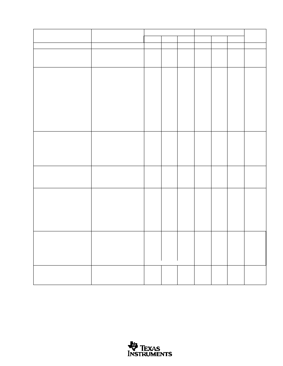
ELECTRICAL CHARACTERISTICS
All specifications T
MIN
to T
MAX
, +V
A
+ V
D
= +5V, and V
REF
= internal +2.5V, f
CLK
= 8MHz, f
SAMPLE
= 500kHz, unless otherwise noted.
ADS7861E
ADS7861EB
PARAMETER
CONDITIONS
MIN
TYP
MAX
MIN
TYP
MAX
UNITS
RESOLUTION
12
Bits
ANALOG INPUT
Input Voltage Range-Bipolar
V
CENTER
= Internal V
REF
at 2.5V
şV
REF
+V
REF
V
Input Capacitance
15
pF
Input Leakage Current
▒
1
Á
A
SYSTEM PERFORMANCE
No Missing Codes
12
Bits
Integral Linearity
▒
0.75
▒
2
▒
0.5
▒
1
LSB
Integral Linearity Match
0.5
▒
1
LSB
Differential Linearity
▒
1
▒
0.5
▒
1
LSB
Bipolar Offset Error
Referenced to REF
IN
▒
0.5
▒
3
LSB
Bipolar Offset Error Match
3
2
LSB
Positive Gain Error
Referenced to REF
IN
▒
0.15
▒
0.75
▒
0.10
▒
0.50
% of FSR
Positive Gain Error Match
2
1
LSB
Negative Gain Error
Referenced to REF
IN
▒
0.15
▒
0.75
▒
0.10
▒
0.50
% of FSR
Negative Gain Error Match
2
1
LSB
Common-Mode Rejection Ratio
At DC
80
dB
V
IN
=
▒
1.25Vp-p at 50kHz
80
dB
Noise
120
Á
Vrms
Power Supply Rejection Ratio
0.5
2
LSB
SAMPLING DYNAMICS
Conversion Time per A/D
1.625
Á
s
Acquisition Time
0.375
Á
s
Throughput Rate
500
kHz
Aperture Delay
3.5
ns
Aperture Delay Matching
100
ps
Aperture Jitter
50
ps
Small-Signal Bandwidth
40
MHz
DYNAMIC CHARACTERISTICS
Total Harmonic Distortion
V
IN
=
▒
2.5Vp-p at 100kHz
ş72
ş76
dB
SINAD
V
IN
=
▒
2.5Vp-p at 100kHz
70
dB
Spurious Free Dynamic Range
V
IN
=
▒
2.5Vp-p at 100kHz
72
76
dB
Channel-to-Channel Isolation
V
IN
=
▒
2.5Vp-p at 100kHz
ş80
dB
VOLTAGE REFERENCE
Internal
2.475
2.5
2.525
V
Internal Drift
▒
25
ppm/
░
C
Internal Noise
50
Á
Vp-p
Internal Source Current
2
mA
Internal Load Rejection
0.005
mV/
Á
A
Internal PSRR
80
dB
External Voltage Range
1.2
2.5
2.6
V
Input Current
0.05
1
Á
A
Input Capacitance
5
pF
DIGITAL INPUT/OUTPUT
Logic Family
CMOS
Logic Levels: V
IH
I
IH
= +5
Á
A
3.0
+V
DD
+ 0.3
V
V
IL
I
IL
= +5
Á
A
ş0.3
1
V
V
OH
I
OH
= ş0.5mA
3.5
V
V
OL
I
OL
= ş0.5mA
0.4
V
External Clock, Optional
0.2
8
MHz
Data Format
Binary Two's Complement
POWER SUPPLY REQUIREMENTS
Power Supply Voltage, +V
4.75
5
5.25
V
Quiescent Current, +V
A
5
8
mA
Power Dissipation
25
40
mW
Specifications same as ADS7861E.

ADS7861
4
SBAS110A
PIN
NAME
DESCRIPTION
1
DGND
Digital Ground. Connect directly to analog ground (pin 12).
2
CH B1+
Non-Inverting Input Channel B1
3
CH B1ş
Inverting Input Channel B1
4
CH B0+
Non-Inverting Input Channel B0
5
CH B0ş
Inverting Input Channel B0
6
CH A1+
Non-Inverting Input Channel A1
7
CH A1ş
Inverting Input Channel A1
8
CH A0+
Non-Inverting Input Channel A0
9
CH A0ş
Inverting Input Channel A0
10
REF
IN
Reference Input
11
REF
OUT
2.5V Reference Output
12
AGND
Analog Ground. Connect directly to digital ground (pin 1).
13
+V
A
Analog Power Supply, +5VDC. Connect directly to digital
power supply (pin 24). Decouple to analog ground with a
0.1
Á
F ceramic capacitor and a 10
Á
F tantalum capacitor.
14
M1
Selects between the Serial Outputs. When M1 is LOW,
both Serial Output A and Serial Output B are selected for
data transfer. When M1 is HIGH, Serial output A is
configured for both Channel A data and Channel B data;
Serial Output B goes into tri-state (i.e., high impedance).
15
M0
Selects between two-channel and four-channel opera-
tion. When M0 is LOW, two-channel operation is se-
lected and operates in conjunction with A0. When A0 is
HIGH, Channel A1 and Channel B1 are being con-
verted. When A0 is LOW, Channel A0 and Channel B0
are being converted. When M0 is HIGH, four-channel
operation is selected. In this mode, all four channels are
converted in sequence starting with Channels A0 and
B0, followed by Channels A1 and B1.
16
A0
A0 operates in conjunction with M0. With M0 LOW and
A0 HIGH, Channel A1 and Channel B1 are converted.
With M0 LOW and A0 LOW, Channel A0 and Channel
B0 are converted.
17
CONVST
Convert Start. When CONVST switches from LOW to
HIGH, the device switches from the sample to hold
mode, independent of the status of the external clock.
18
RD
Synchronization Pulse for the Serial Output.
19
CS
Chip Select. When LOW, the Serial Output A and Serial
Output B outputs are active; when HIGH, the serial
outputs are tri-stated.
20
CLOCK
An external CMOS-compatible clock can be applied to
the CLOCK input to synchronize the conversion process
to an external source. The CLOCK pin controls the
sampling rate by the equation: CLOCK = 16 Ě f
SAMPLE
.
21
BUSY
BUSY goes HIGH during a conversion and returns LOW
after the third LSB has been transmitted on either the
Serial A or Serial B output pin.
22
SERIAL
The Serial Output data word is comprised of channel
information and 12 bits of data. In operation, data is valid
on the falling edge of DCLOCK for 16 edges after the
rising edge of the RD.
23
SERIAL
The Serial Output data word is comprised of channel
information and 12 bits of data. In operation, data is valid
on the falling edge of DCLOCK for 16 edges after the
rising edge of the RD. When M1 is HIGH, both Channel
A data and Channel B data are available.
24
+V
D
Digital Power Supply, +5VDC. Connect directly to pin
13. Must be
+V
A
.
PIN CONFIGURATION
Top View
SSOP
PIN DESCRIPTIONS
DATA
B
DATA
A
DGND
CH B1+
CH B1ş
CH B0+
CH B0ş
CH A1+
CH A1ş
CH A0+
CH A0ş
REF
IN
REF
OUT
AGND
1
2
3
4
5
6
7
8
9
10
11
12
24
23
22
21
20
19
18
17
16
15
14
13
+V
D
SERIAL DATA A
SERIAL DATA B
BUSY
CLOCK
CS
RD
CONVST
A0
M0
M1
+V
A
ADS7861

ADS7861
5
SBAS110A
TYPICAL CHARACTERISTICS
At T
A
= +25
░
C, +V
A
+ V
D
= +5V, and V
REF
= internal +2.5V, f
CLK
= 8MHz, f
SAMPLE
= 500kHz, unless otherwise noted.
FREQUENCY SPECTRUM
(4096 Point FFT; f
IN
= 99.9kHz, ş0.5dB)
Frequency (kHz)
0
ş20
ş40
ş60
ş80
ş100
ş120
Amplitude (dB)
0
62.5
125
250
187.5
FREQUENCY SPECTRUM
(4096 Point FFT; f
IN
= 199.9kHz, ş0.5dB)
Frequency (kHz)
0
ş20
ş40
ş60
ş80
ş100
ş120
Amplitude (dB)
0
62.5
125
250
187.5
CHANGE IN POSITIVE GAIN MATCH
vs TEMPERATURE
(Maximum Deviation for All Four Channels)
Temperature (
░
C)
0.6
0.5
0.4
0.3
0.2
0.1
0
Change in Positive Gain Match (LSB)
ş40
25
85
150
CHANGE IN SIGNAL-TO-NOISE RATIO
AND SIGNAL-TO-(NOISE+DISTORTION)
vs TEMPERATURE
Temperature (
░
C)
0.7
0.6
0.5
0.4
0.3
0.2
0.1
0
ş0.1
Delta from +25
░
C (dB)
ş40
25
85
SNR
SINAD
CHANGE IN SPURIOUS FREE DYNAMIC RANGE
AND TOTAL HARMONIC DISTORTION
vs TEMPERATURE
Temperature (
░
C)
7
6
5
4
3
2
1
0
ş1
+1
0
ş0.5
ş1
ş1.5
ş2
ş2.5
ş3
ş3.5
SFDR Delta from +25
░
C (dB)
THD Delta from +25
░
C (dB)
ş40
25
85
THD
SFDR
SIGNAL-TO-NOISE RATIO and
SIGNAL-TO-(NOISE+DISTORTION)
vs INPUT FREQUENCY
10k
100k
1k
1M
Input Frequency (Hz)
SNR and SINAD (dB)
74
72
70
68
66
64
76
SINAD
SNR