Äîêóìåíòàöèÿ è îïèñàíèÿ www.docs.chipfind.ru
www.ti.com
PRODUCT PREVIEW
FEATURES
APPLICATIONS
DESCRIPTION
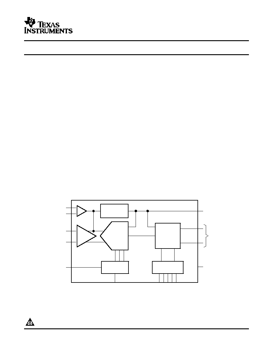
CLKP
CLKM
INP
INM
VCMOUT/
REFIN
PLL
SH
14-Bit ADC
REFERENCE
CLKOUT
OVR
IREF
SCLK
SEN
SDA
T
A
RESET
OE
D13-D0
IN CMOS MODE
DIGITAL
ENCODER
CONTROL I/F
ADS5545
SLWS180 SEPTEMBER 2005
14-BITS, 170 MSPS ADC WITH LVDS/CMOS OUTPUTS
·
Wireless Communication
·
Maximum Sample Rate: 170 MSPS
·
Software Defined Radio
·
14-Bit Resolution
·
Power Amplifier Linearization
·
No Missing Codes
·
802.16d/e
·
Power Dissipation
·
Test and Measurement Instrumentation
Core Power: 1 W
·
High Definition Video
Total Power: 1.22 W
·
Medical Imaging
·
Internal Sample and Hold
·
Radar Systems
·
73.5-dBFS SNR at 70-MHz IF
·
85-dBc SFDR at 70-MHz IF
·
Parallel CMOS and LVDS Output Options
·
Internal Reference, External Reference
Support
·
3.3-V Analog and Digital Supply
·
48-Pin QFN Package (7 mm
×
7 mm)
The ADS5545 is a high performance 14-bit 170-MSPS ADC. Using an internal sample and hold and low jitter
clock buffer this ADC supports high SNR and high SFDR at high IF. With programmable options for parallel
CMOS and LVDS outputs, this device is available in a compact 48-pin QFN package. The device provides
internal references or can optionally be driven with an external reference. The device is specified over a 40
°
C to
85
°
C operating range.
Please be aware that an important notice concerning availability, standard warranty, and use in critical applications of Texas
Instruments semiconductor products and disclaimers thereto appears at the end of this data sheet.
PRODUCT PREVIEW information concerns products in the
Copyright © 2005, Texas Instruments Incorporated
formative or design phase of development. Characteristic data and
other specifications are design goals. Texas Instruments reserves
the right to change or discontinue these products without notice.
www.ti.com
PRODUCT PREVIEW
ABSOLUTE MAXIMUM RATINGS
(1)
RECOMMENDED OPERATING CONDITIONS
ELECTRICAL CHARACTERISTICS
ADS5545
SLWS180 SEPTEMBER 2005
PACKAG/ORDERING INFORMATION
(1)
SPECIFIED
PACKAGE
ORDERING
TRANSPORT
PACKAGE-
PACKAGE
PRODUCT
TEMPERATURE
MARKING
NUMBER
MEDIA,
LEAD
DESIGNATOR
RANGE
QUANTITY
ADS5545
48-QFN
RGZ
40
°
C to 85
°
C
ADS5545IRGZ
(1)
JA
= TBD,
JC
= TBD
VALUE
UNIT
AVDD
Supply voltage range
0.3 V to 3.9
V
DRVDD Supply voltage range
0.3 V to 3.9
V
Voltage between AGND and DRGND
0.3 to 0.3
V
Voltage between AVDD to DRVDD
0.3 to 3.3
V
CM
Voltage applied to external pin
0.3 to 2
V
Voltage applied to analog input pins
0.3 V to minimum (3.6, AVDD + 0.3 V )
V
T
A
Operating free-air temperature range
40 to 85
°
C
T
J
Operating junction temperature range
125
°
C
T
stg
Storage temperature range
65
to 150
°
C
Lead temperature 1,6 mm (1/16 inch) from the case for 10 seconds
220
°
C
(1)
Stresses beyond those listed under absolute maximum ratings may cause permanent damage to the device. These are stress ratings
only, and functional operation of the device at these or any other conditions beyond those indicated under recommended operating
conditions is not implied. Exposure to absolute-maximum-rated conditions for extended periods may affect device reliability.
MIN
NOM
MAX
UNIT
SUPPLIES AND REFERENCES
AVDD
Analog supply voltage
3
3.3
3.6
V
DRVDD
Digital supply voltage
3
3.3
3.6
V
CLOCK INPUT
Input clock sample rate
1
170
MSPS
Input clock amplitude, differential
Vpp
Input clock duty cycle
50%
Operating free-air temperature
40
85
°
C
Typical values at 25
°
C, min, max values are across the full temperature range T
MIN
= 40
°
C to T
MAX
= 85
°
C, AVDD = DRVDD
= 3.3 V, sampling rate = 170 MSPS, 50% clock duty cycle, 1 dBFS differential analog input, internal reference mode, LVDS
data output (unless otherwise noted)
PARAMETER
TEST CONDITIONS
MIN
TYP
MAX
UNIT
DC ACCURACY
Resolution
14
bits
No missing codes
Assured
DNL
Differential non-linearity
0.9
0.5
TBD
LSB
INL
Integral non-linearity
±
3
LSB
Offset error
±
10
mV
Offset temperature coefficient
TBD
ppm/
°
C
Gain error
±
1
%FS
Gain temperature coefficient
TBD
/
°
C
2
www.ti.com
PRODUCT PREVIEW
ADS5545
SLWS180 SEPTEMBER 2005
ELECTRICAL CHARACTERISTICS (continued)
Typical values at 25
°
C, min, max values are across the full temperature range T
MIN
= 40
°
C to T
MAX
= 85
°
C, AVDD = DRVDD
= 3.3 V, sampling rate = 170 MSPS, 50% clock duty cycle, 1 dBFS differential analog input, internal reference mode, LVDS
data output (unless otherwise noted)
PARAMETER
TEST CONDITIONS
MIN
TYP
MAX
UNIT
POWER SUPPLY
ICC
Total supply current
F
IN
= TBD
369
mA
IAVDD
Analog supply current
F
IN
= TBD
315
mA
LVDS mode, F
IN
= TBD, C
L
= 5 pF
54
mA
IDRVDD
Digital supply current
CMOS mode, F
IN
= TBD, C
L
= 5 pF
70
mA
Total power dissipation
LVDS mode, F
IN
= TBD
1.22
W
Power down dissipation
Clock running
TBD
mW
REFERENCE VOLTAGES
VREFB
Reference bottom
0.5
V
VREFT
Reference top
2.5
V
VCM
Common mode voltage (internal)
1.5
V
VCM output current
±
4
mA
ANALOG INPUT
Differential input capacitance
7
pF
Analog input common mode range
VCM
±
0.1
V
Differential input voltage range
2
Vpp
Analog input bandwidth
3 dB, source impedance 50
400
MHz
DYNAMIC AC CHARACTERISTICS
F
IN
= 10 MHz
90
SFDR
Spurious free dynamic range
F
IN
= 70 MHz
85
dBc
F
IN
= 150 MHz
84
F
IN
= 10 MHz
74
SNR
Signal-to-noise ratio
F
IN
= 70 MHz
73.5
dBFS
F
IN
= 150 MHz
72
3
www.ti.com
PRODUCT PREVIEW
DIGITAL CHARACTERISTICS
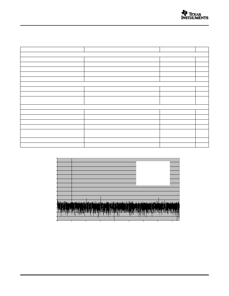
-150
-140
-130
-120
-110
-100
-90
-80
-70
-60
-50
-40
-30
-20
-10
0
0
10
20
30
40
50
60
70
80
F
S
= 170 MSPS
F
IN
= 10.1 MHz
SFDR = 91.5 dBc
SNR = 74.09
dBFS
ADS5545
SLWS180 SEPTEMBER 2005
The dc specifications refer to the condition where the digital outputs are not switching, but are permanently at a valid logic
level 0 or 1 AVDD = DRVDD = 3.3 V, I
O
= 3.5 mA, R
L
= 100
.
(1)
All LVDS and CMOS specifications are characterized, but not tested at production.
PARAMETER
TEST CONDITIONS
MIN
TYP
MAX
UNIT
DIGITAL INPUTS
High-level input voltage
2.4
V
Low-level input voltage
0.8
V
High-level input current
10
µ
A
Low-level input current
10
µ
A
Input capacitance
4
pF
DIGITAL OUTPUTS CMOS MODE
High-level output voltage
3.3
V
Low-level output voltage
0
V
Output capacitance
Output capacitance inside the device, from either
4
pF
output to ground
DIGITAL OUTPUTS LVDS MODE
High-level output voltage
1375
mV
Low-level output voltage
1025
mV
Output differential voltage, |V
OD
|
350
mV
V
OS
Output offset voltage
(1)
Common-mode voltage of OUTP and OUTM
1200
mV
Output capacitance
Output capacitance inside the device, from either
4
pF
output to ground
Change in |V
OD
|, |
V
OD
|
25
mV
Change in |V
OS
|, |
V
OS
|
25
mV
(1)
I
O
refers to the LVDS buffer current setting, R
L
is the differential load resistance between the LVDS output pair.
Figure 1. ADS5545 FFT Plot at 170 MSPS and 10-MHz Input
4
www.ti.com
PRODUCT PREVIEW
-150
-140
-130
-120
-110
-100
-90
-80
-70
-60
-50
-40
-30
-20
-10
0
0
10
20
30
40
50
60
70
80
F
S
= 170 MSPS
F
IN
= 70.1 MHz
SFDR = 87.8 dBc
SNR = 73.5 dBFS
ADS5545
SLWS180 SEPTEMBER 2005
Figure 2. ADS5545 FFT Plot at 170 MSPS and 70-MHz Input
5
Document Outline