Äîêóìåíòàöèÿ è îïèñàíèÿ www.docs.chipfind.ru
8-Channel, 24-Bit
ANALOG-TO-DIGITAL CONVERTER
FEATURES
q
24 BITS NO MISSING CODES
q
0.0015% INL
q
22 BITS EFFECTIVE RESOLUTION
(PGA = 1), 19 BITS (PGA = 128)
q
PGA FROM 1 TO 128
q
SINGLE CYCLE SETTLING MODE
q
PROGRAMMABLE DATA OUTPUT RATES
UP TO 1kHz
q
ON-CHIP 1.25V/2.5V REFERENCE
q
EXTERNAL DIFFERENTIAL REFERENCE
OF 0.1V TO 2.5V
q
ON-CHIP CALIBRATION
q
SPITM COMPATIBLE
q
2.7V TO 5.25V
q
< 1mW POWER CONSUMPTION
DESCRIPTION
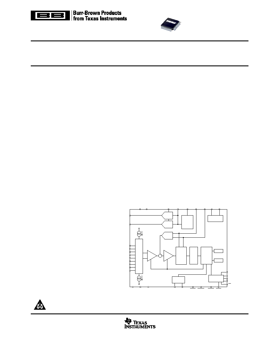
The ADS1216 is a precision, wide dynamic range, delta-sigma, Analog-
to-Digital (A/D) converter with 24-bit resolution operating from 2.7V to
5.25V supplies. The delta-sigma, A/D converter provides up to 24 bits of
no missing code performance and effective resolution of 22 bits.
The eight input channels are multiplexed. Internal buffering can be
selected to provide a very high input impedance for direct connection to
transducers or low-level voltage signals. Burn out current sources are
provided that allow for the detection of an open or shorted sensor. An 8-
bit Digital-to-Analog (D/A) converter provides an offset correction with
a range of 50% of the FSR (Full-Scale Range).
The PGA (Programmable Gain Amplifier) provides selectable gains
of 1 to 128 with an effective resolution of 19 bits at a gain of 128.
The A/D conversion is accomplished with a second-order delta-
sigma modulator and programmable sinc filter. The reference input
is differential and can be used for ratiometric cancellation. The on-
board current DACs (Digital-to-Analog Converters) operate inde-
pendently with the maximum current set by an external resistor.
The serial interface is SPI compatible. Eight bits of digital I/O are
also provided that can be used for input or output. The ADS1216 is
designed for high-resolution measurement applications in smart
transmitters, industrial process control, weight scales, chromatogra-
phy, and portable instrumentation.
APPLICATIONS
q
INDUSTRIAL PROCESS CONTROL
q
LIQUID/GAS CHROMATOGRAPHY
q
BLOOD ANALYSIS
q
SMART TRANSMITTERS
q
PORTABLE INSTRUMENTATION
q
WEIGHT SCALES
q
PRESSURE TRANSDUCERS
ADS1
216
SPI is a registered trademark of Motorola.
BUF
PGA
A = 1:128
+
1.25V or
2.5V
Reference
Clock Generator
Registers
Serial Interface
2nd-Order
Modulator
RAM
Digital I/O
Interface
AGND
AV
DD
IN+
IN
R
DAC
V
REFOUT
V
RCAP
V
REF+
V
REF
X
IN
X
OUT
DSYNC
PDWN
RESET
DRDY
D7
BUFEN
DGND
DV
DD
...
D0
SCLK
POL
D
IN
D
OUT
CS
MUX
A
IN
0
A
IN
1
A
IN
2
A
IN
3
A
IN
4
A
IN
5
A
IN
6
A
IN
7
A
INCOM
IDAC1
Controller
Program-
mable
Digital
Filter
2
µ
A
AV
DD
8-Bit
IDAC
IDAC2
8-Bit
IDAC
Offset
DAC
AGND
2
µ
A
ADS1216
SBAS171B JUNE 2001
www.ti.com
PRODUCTION DATA information is current as of publication date.
Products conform to specifications per the terms of Texas Instruments
standard warranty. Production processing does not necessarily include
testing of all parameters.
Copyright © 2000, Texas Instruments Incorporated
Please be aware that an important notice concerning availability, standard warranty, and use in critical applications of
Texas Instruments semiconductor products and disclaimers thereto appears at the end of this data sheet.
ADS1216
2
SBAS171B
ELECTRICAL CHARACTERISTICS: AV
DD
= 5V
All specifications T
MIN
to T
MAX
, AV
DD
= +5V, DV
DD
= +2.7V to 5.25V, f
MOD
= 19.2kHz, PGA = 1, Buffer ON, R
DAC
= 150k
, f
DATA
= 10Hz,
V
REF
(REF IN+) (REF IN) = +2.5V, unless otherwise specified.
AV
DD
to AGND ...................................................................... 0.3V to +6V
DV
DD
to DGND ...................................................................... 0.3V to +6V
Input Current ............................................................... 100mA, Momentary
Input Current ................................................................. 10mA, Continuous
A
IN
................................................................... GND 0.5V to AV
DD
+ 0.5V
AV
DD
to DV
DD
........................................................................... 6V to +6V
AGND to DGND ................................................................. 0.3V to +0.3V
Digital Input Voltage to GND .................................... 0.3V to DV
DD
+ 0.3V
Digital Output Voltage to GND ................................. 0.3V to DV
DD
+ 0.3V
Maximum Junction Temperature ................................................... +150
°
C
Operating Temperature Range ......................................... 40
°
C to +85
°
C
Storage Temperature Range .......................................... 60
°
C to +100
°
C
Lead Temperature (soldering, 10s) .............................................. +300
°
C
NOTE: (1) Stresses above those listed under "Absolute Maximum Ratings" may
cause permanent damage to the device. Exposure to absolute maximum
conditions for extended periods may affect device reliability.
ABSOLUTE MAXIMUM RATINGS
(1)
PACKAGE
SPECIFIED
DRAWING
TEMPERATURE
PACKAGE
ORDERING
TRANSPORT
PRODUCT
PACKAGE
NUMBER
RANGE
MARKING
NUMBER
(1)
MEDIA
ADS1216Y
TQFP-48
PFB
40 to +85
ADS1216Y
ADS1216Y/250
Tape and Reel
"
"
"
"
"
ADS1216Y/2K
Tape and Reel
NOTE: (1) Models with a slash (/) are available only in Tape and Reel in the quantities indicated (e.g., / 2K indicates 2000 devices per reel). Ordering 2000 pieces
of "ADS1216Y/2K" will get a single 2000-piece Tape and Reel.
PACKAGE/ORDERING INFORMATION
ADS1216
PARAMETER
CONDITIONS
MIN
TYP
MAX
UNITS
ANALOG INPUT (A
IN
0 A
IN
7, A
INCOM
)
Analog Input Range
Buffer OFF
AGND 0.1
AV
DD
+ 0.1
V
Buffer ON
AGND + 0.05
AV
DD
1.5
V
Full-Scale Input Voltage Range
(In+) (In), See Block Diagram
±
V
REF
/PGA
V
Differential Input Impedance
Buffer OFF
5/PGA
M
Input Current
Buffer ON
0.5
nA
Bandwidth
Fast Settling Filter
3dB
0.469 · f
DATA
Hz
Sinc
2
Filter
3dB
0.318 · f
DATA
Hz
Sinc
3
Filter
3dB
0.262 · f
DATA
Hz
Programmable Gain Amplifier
User Selectable Gain Ranges
1
128
Input Capacitance
9
pF
Input Leakage Current
Modulator OFF, T = 25
°
C
5
pA
Burnout Current Sources
2
µ
A
OFFSET DAC
Offset DAC Range
±
V
REF
/(2 · PGA)
V
Offset DAC Monotonicity
8
Bits
Offset DAC Gain Error
±
10
%
Offset DAC Gain Error Drift
1
ppm/
°
C
SYSTEM PERFORMANCE
Resolution
24
Bits
No Missing Codes
sinc
3
Filter
24
Bits
Integral Non-Linearity
End Point Fit
±
0.0015
% of FS
Offset Error
(1)
7.5
ppm of FS
Offset Drift
(1)
0.02
ppm of FS/
°
C
Gain Error
(1)
0.005
%
Gain Error Drift
(1)
0.5
ppm/
°
C
Common-Mode Rejection
at DC
100
dB
f
CM
= 60Hz, f
DATA
= 10Hz
130
dB
f
CM
= 50Hz, f
DATA
= 50Hz
120
dB
f
CM
= 60Hz, f
DATA
= 60Hz
120
dB
Normal-Mode Rejection
f
SIG
= 50Hz, f
DATA
= 50Hz
100
dB
f
SIG
= 60Hz, f
DATA
= 60Hz
100
dB
Output Noise
See Typical Characteristics
Power-Supply Rejection
at DC, dB = 20 log(
V
OUT
/
V
DD
)
(2)
80
95
dB
ELECTROSTATIC
DISCHARGE SENSITIVITY
This integrated circuit can be damaged by ESD. Texas Instru-
ments recommends that all integrated circuits be handled with
appropriate precautions. Failure to observe proper handling
and installation procedures can cause damage.
ESD damage can range from subtle performance degradation
to complete device failure. Precision integrated circuits may
be more susceptible to damage because very small parametric
changes could cause the device not to meet its published
specifications.
3
ADS1216
SBAS171B
ELECTRICAL CHARACTERISTICS: AV
DD
= 5V
(Cont.)
All specifications T
MIN
to T
MAX
, AV
DD
= +5V, DV
DD
= +2.7V to 5.25V, f
MOD
= 19.2kHz, PGA = 1, Buffer ON, R
DAC
= 150k
, f
DATA
= 10Hz,
V
REF
(REF IN+) (REF IN) = +2.5V, unless otherwise specified.
ADS1216
PARAMETER
CONDITIONS
MIN
TYP
MAX
UNITS
VOLTAGE REFERENCE INPUT
Reference Input Range
REF IN+, REF IN
AGND
AV
DD
V
V
REF
V
REF
(REF IN+) (REF IN)
0.1
2.5
2.6
V
Common-Mode Rejection
at DC
120
dB
Common-Mode Rejection
f
VREFCM
= 60Hz, f
DATA
= 60Hz
120
dB
Bias Current
(3)
V
REF
= 2.5V
1.3
µ
A
ON-CHIP VOLTAGE REFERENCE
Output Voltage
REF HI = 1
2.4
2.50
2.6
V
REF HI = 0
1.25
V
Short-Circuit Current Source
8
mA
Short-Circuit Current Sink
50
µ
A
Short-Circuit Duration
Sink or Source
Indefinite
Drift
15
ppm/
°
C
Noise
V
RCAP
= 0.1
µ
F, BW = 0.1Hz to 100Hz
10
µ
Vp-p
Output Impedance
Sourcing 100
µ
A
3
Startup Time
50
µ
s
IDAC
Full-Scale Output Current
R
DAC
= 150k
, Range = 1
0.5
mA
R
DAC
= 150k
, Range = 2
1
mA
R
DAC
= 150k
, Range = 3
2
mA
R
DAC
= 15k
, Range = 3
20
mA
Maximum Short-Circuit Current Duration
R
DAC
= 10k
Indefinite
R
DAC
= 0
10
Minute
Monotonicity
R
DAC
= 150k
8
Bits
Compliance Voltage
0
AV
DD
1
V
Output Impedance
See Typical Characteristics
PSRR
V
OUT
= AV
DD
/2
400
ppm/V
Absolute Error
Individual IDAC
5
%
Absolute Drift
Individual IDAC
75
ppm/
°
C
Mismatch Error
Between IDACs, Same Range and Code
0.25
%
Mismatch Drift
Between IDACs, Same Range and Code
15
ppm/
°
C
POWER-SUPPLY REQUIREMENTS
Power-Supply Voltage
AV
DD
4.75
5.25
V
Analog Current (I
ADC
+ I
VREF
+ I
DAC
)
PDWN = 0, or SLEEP
1
nA
ADC Current (I
ADC
)
PGA = 1, Buffer OFF
140
225
µ
A
PGA = 128, Buffer OFF
430
650
µ
A
PGA = 1, Buffer ON
180
275
µ
A
PGA = 128, Buffer ON
800
1250
µ
A
V
REF
Current (I
VREF
)
250
375
µ
A
I
DAC
Current (I
DAC
)
Excludes Load Current
480
675
µ
A
Digital Current
Normal Mode, DV
DD
= 5V
180
275
µ
A
SLEEP Mode, DV
DD
= 5V
150
µ
A
Read Data Continuous Mode, DV
DD
= 5V
230
µ
A
PDWN
1
nA
Power Dissipation
PGA = 1, Buffer OFF, REFEN = 0,
1.6
2.5
mW
I
DACS
OFF, DV
DD
= 5V
TEMPERATURE RANGE
Operating
40
+85
°
C
Storage
60
+100
°
C
NOTES: (1) Calibration can minimize these errors. (2)
V
OUT
is change in digital result. (3) 12pF switched capacitor at f
SAMP
clock frequency.

ADS1216
4
SBAS171B
ELECTRICAL CHARACTERISTICS: AV
DD
= 3V
All specifications T
MIN
to T
MAX
, AV
DD
= +3V, DV
DD
= +2.7V to 5.25V, f
MOD
= 19.2kHz, PGA = 1, Buffer ON, R
DAC
= 75k
, f
DATA
= 10Hz,
V
REF
(REF IN+) (REF IN) = +1.25V unless otherwise specified.
ADS1216
PARAMETER
CONDITIONS
MIN
TYP
MAX
UNITS
ANALOG INPUT (A
IN
0 A
IN
7, A
INCOM
)
Analog Input Range
Buffer OFF
AGND 0.1
AV
DD
+ 0.1
V
Buffer ON
AGND + 0.05
AV
DD
1.5
V
Full-Scale Input Voltage Range
(In+) (In) See Block Diagram
±
V
REF
/PGA
V
Input Impedance
Buffer OFF
5/ PGA
M
Input Current
Buffer ON
0.5
nA
Bandwidth
Fast Settling Filter
3dB
0.469 · f
DATA
Hz
Sinc
2
Filter
3dB
0.318 · f
DATA
Hz
Sinc
3
Filter
3dB
0.262 · f
DATA
Hz
Programmable Gain Amplifier
User Selectable Gain Ranges
1
128
Input Capacitance
9
pF
Input Leakage Current
Modulator OFF, T = 25
°
C
5
pA
Burnout Current Sources
2
µ
A
OFFSET DAC
Offset DAC Range
±
V
REF
/(2 · PGA)
V
Offset DAC Monotonicity
8
Bits
Offset DAC Gain Error
±
10
%
Offset DAC Gain Error Drift
2
ppm/
°
C
SYSTEM PERFORMANCE
Resolution
24
Bits
No Missing Codes
sinc
3
Filter
24
Bits
Integral Non-Linearity
End Point Fit
±
0.0015
% of FS
Offset Error
(1)
15
ppm of FS
Offset Drift
(1)
0.04
ppm of FS/
°
C
Gain Error
(1)
0.010
%
Gain Error Drift
(1)
1.0
ppm/
°
C
Common-Mode Rejection
at DC
100
dB
f
CM
= 60Hz, f
DATA
= 10Hz
130
dB
f
CM
= 50Hz, f
DATA
= 50Hz
120
dB
f
CM
= 60Hz, f
DATA
= 60Hz
120
dB
Normal-Mode Rejection
f
SIG
= 50Hz, f
DATA
= 50Hz
100
dB
f
SIG
= 60Hz, f
DATA
= 60Hz
100
dB
Output Noise
See Typical Characteristics
Power-Supply Rejection
at DC, dB = 20 log(
V
OUT
/
V
DD
)
(2)
75
90
dB
VOLTAGE REFERENCE INPUT
Reference Input Range
REF IN+, REF IN
0
AV
DD
V
V
REF
V
REF
(REF IN+) (REF IN)
0.1
1.25
1.3
V
Common-Mode Rejection
at DC
120
dB
Common-Mode Rejection
f
VREFCM
= 60Hz, f
DATA
= 60Hz
120
dB
Bias Current
(3)
V
REF
= 1.25V
0.65
µ
A
ON-CHIP VOLTAGE REFERENCE
Output Voltage
REF HI = 0
1.2
1.25
1.3
V
Short-Circuit Current Source
3
mA
Short-Circuit Current Sink
50
µ
A
Short-Circuit Duration
Sink or Source
Indefinite
Drift
15
ppm/
°
C
Noise
V
RCAP
= 0.1
µ
F, BW = 0.1Hz to 100Hz
10
µ
Vp-p
Output Impedance
Sourcing 100
µ
A
3
Startup Time
50
µ
s
IDAC
Full-Scale Output Current
R
DAC
= 75k
, Range = 1
0.5
mA
R
DAC
= 75k
, Range = 2
1
mA
R
DAC
= 75k
, Range = 3
2
mA
R
DAC
= 15k
, Range = 3
20
mA
Maximum Short-Circuit Current Duration
R
DAC
= 10k
Indefinite
R
DAC
= 0
10
Minute
Monotonicity
R
DAC
= 75k
8
Bits
Compliance Voltage
0
AV
DD
1
V
Output Impedance
See Typical Characteristics
PSRR
V
OUT
= AV
DD
/2
600
ppm/V
Absolute Error
Individual IDAC
5
%
Absolute Drift
Individual IDAC
75
ppm/
°
C
Mismatch Error
Between IDACs, Same Range and Code
0.25
%
Mismatch Drift
Between IDACs, Same Range and Code
15
ppm/
°
C
5
ADS1216
SBAS171B
POWER-SUPPLY REQUIREMENTS
Power-Supply Voltage
AV
DD
2.7
3.3
V
Analog Current (I
ADC
+ I
VREF
+ I
DAC
)
PDWN = 0, or SLEEP
1
nA
ADC Current (I
ADC
)
PGA = 1, Buffer OFF
120
200
µ
A
PGA = 128, Buffer OFF
370
600
µ
A
PGA = 1, Buffer ON
170
250
µ
A
PGA = 128, Buffer ON
750
1200
µ
A
V
REF
Current (I
VREF
)
250
375
µ
A
I
DAC
Current (I
DAC
)
Excludes Load Current
480
675
µ
A
Digital Current
Normal Mode, DV
DD
= 3V
90
200
µ
A
SLEEP Mode, DV
DD
= 3V
75
µ
A
Read Data Continuous Mode, DV
DD
= 3V
113
µ
A
PDWN = 0
1
nA
Power Dissipation
PGA = 1, Buffer OFF, REFEN = 0,
0.6
1.2
mW
I
DACS
OFF, DV
DD
= 3V
TEMPERATURE RANGE
Operating
40
+85
°
C
Storage
60
+100
°
C
NOTES: (1) Calibration can minimize these errors. (2)
V
OUT
is change in digital result. (3) 12pF switched capacitor at f
SAMP
clock frequency.
ADS1216
PARAMETER
CONDITIONS
MIN
TYP
MAX
UNITS
ELECTRICAL CHARACTERISTICS: AV
DD
= 3V
(Cont.)
All specifications T
MIN
to T
MAX
, AV
DD
= +3V, DV
DD
= +2.7V to 5.25V, f
MOD
= 19.2kHz, PGA = 1, Buffer ON, R
DAC
= 75k
, f
DATA
= 10Hz,
V
REF
(REF IN+) (REF IN) = +1.25V unless otherwise specified.
PARAMETER
CONDITIONS
MIN
TYP
MAX
UNITS
Digital Input/Output
Logic Family
CMOS
Logic Level: V
IH
0.8 · DV
DD
DV
DD
V
V
IL
DGND
0.2 · DV
DD
V
V
OH
I
OH
= 1mA
DV
DD
0.4
V
V
OL
I
OL
= 1mA
DGND
DGND + 0.4
V
Input Leakage: I
IH
V
I
= DV
DD
10
µ
A
I
IL
V
I
= 0
10
µ
A
Master Clock Rate: f
OSC
1
5
MHz
Master Clock Period: t
OSC
1/f
OSC
200
1000
ns
DIGITAL SPECIFICATIONS: T
MIN
to T
MAX
, DV
DD
2.7V to 5.25V