74AC11378
HEX DÙTYPE FLIPÙFLOP
WITH CLOCK ENABLE
SCAS150 Ù APRIL 1991 Ù REVISED APRIL 1993
Copyright
ˋ
1993, Texas Instruments Incorporated
1
POST OFFICE BOX 655303
ñ
DALLAS, TEXAS 75265
POST OFFICE BOX 1443
ñ
HOUSTON, TEXAS 77251Ù1443
ñ
Contains Six D-Type Flip-Flops
ñ
Clock Enable Latched to Avoid False
Clocking
ñ
Applications Include: Buffer/Storage
Registers, Shift Registers, Pattern
Generators
ñ
Flow-Through Architecture Optimizes PCB
Layout
ñ
Center-Pin V
CC
and GND Pin Configurations
Minimize High-Speed Switching Noise
ñ
EPIC
TM
(Enhanced-Performance Implanted
CMOS) 1-
ç
m Process
ñ
500-mA Typical Latch-Up Immunity at 125
¯
C
ñ
Package Options Include Plastic
Small-Outline Packages, and Standard
Plastic 300-mil DIPs
description
These circuits are positive-edge-triggered D-type flip-flops with a clock-enable input. Information at the D inputs
meeting the setup time requirements is transferred to the Q outputs on the positive-going edge of the clock pulse
if the clock-enable input (CLKEN) is low.
Clock triggering occurs at a particular voltage level and is not directly related to the transition time of the
positive-going pulse. When the clock inputs are at either the high or low level, the data (D) input signal has no
effect at the output. The circuits are designed to prevent false clocking by transitions at the clock-enable
(CLKEN) input.
The 74AC11378 is characterized for operation from Ù 40
¯
C to 85
¯
C.
FUNCTION TABLE
(each flip-flop)
INPUTS
OUTPUT
CLKEN
CLK
D
OUTPUT
Q
H
X
X
QO
L
H
H
L
L
L
X
L
X
QO
PRODUCTION DATA information is current as of publication date.
Products conform to specifications per the terms of Texas Instruments
standard warranty. Production processing does not necessarily include
testing of all parameters.
EPIC is a trademark of Texas Instruments Incorporated.
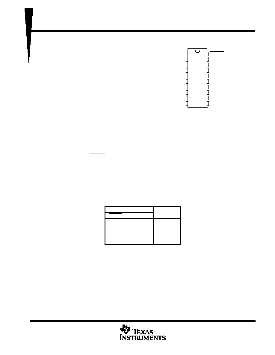
1
2
3
4
5
6
7
8
9
10
20
19
18
17
16
15
14
13
12
11
1Q
2Q
3Q
GND
GND
GND
GND
4Q
5Q
6Q
CLKEN
1D
2D
3D
V
CC
V
CC
4D
5D
6D
CLK
DW OR N PACKAGE
(TOP VIEW)
74AC11378
HEX DÙTYPE FLIPÙFLOP
WITH CLOCK ENABLE
SCAS150 Ù APRIL 1991 Ù REVISED APRIL 1993
2
POST OFFICE BOX 655303
ñ
DALLAS, TEXAS 75265
POST OFFICE BOX 1443
ñ
HOUSTON, TEXAS 77251Ù1443
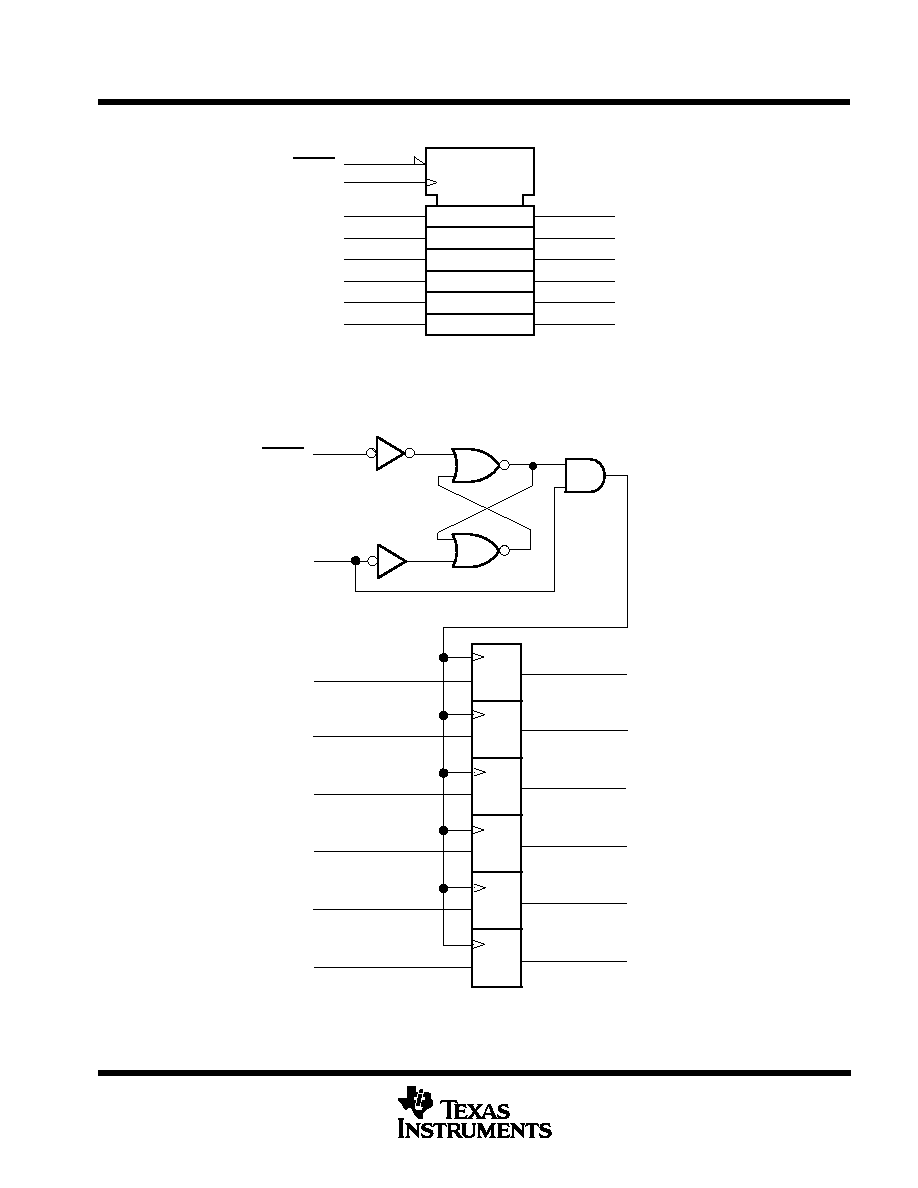
logic symbol
This symbol is in accordance with ANSI/IEEE Std 91-1984 and
IEC Publication 617-12.
2D
19
1D
18
2D
17
3D
G1
20
11
CLK
1Q
1
2Q
2
3Q
3
14
4D
13
5D
12
6D
4Q
8
5Q
9
6Q
10
CLKEN
1C2
logic diagram (positive logic)
CLKEN
1Q
1
C1
1D
1D
19
2Q
2
C1
1D
2D
18
3Q
3
C1
1D
3D
17
4Q
8
C1
1D
4D
14
5Q
9
C1
1D
5D
13
6Q
10
C1
1D
6D
12
CLK
11
20
74AC11378
HEX DÙTYPE FLIPÙFLOP
WITH CLOCK ENABLE
SCAS150 Ù APRIL 1991 Ù REVISED APRIL 1993
3
POST OFFICE BOX 655303
ñ
DALLAS, TEXAS 75265
POST OFFICE BOX 1443
ñ
HOUSTON, TEXAS 77251Ù1443
absolute maximum ratings over operating free-air temperature range (unless otherwise noted)
Supply voltage range, V
CC
Ù 0.5 V to 7 V
. . . . . . . . . . . . . . . . . . . . . . . . . . . . . . . . . . . . . . . . . . . . . . . . . . . . . . . . . .
Input voltage range, V
I
(see Note 1)
Ù 0.5 V to V
CC
+ 0.5 V
. . . . . . . . . . . . . . . . . . . . . . . . . . . . . . . . . . . . . . . . . .
Output voltage range, V
O
(see Note 1)
Ù 0.5 V to V
CC
+ 0.5 V
. . . . . . . . . . . . . . . . . . . . . . . . . . . . . . . . . . . . . . .
Input clamp current, I
IK
(V
I
< 0 or V
I
> V
CC
)
Ý
20 mA
. . . . . . . . . . . . . . . . . . . . . . . . . . . . . . . . . . . . . . . . . . . . . . .
Output clamp current, I
OK
(V
O
< 0 or V
O
> V
CC
)
Ý
50 mA
. . . . . . . . . . . . . . . . . . . . . . . . . . . . . . . . . . . . . . . . . . .
Continuous output current, I
O
(V
O
= 0 to V
CC
)
Ý
50 mA
. . . . . . . . . . . . . . . . . . . . . . . . . . . . . . . . . . . . . . . . . . . . . .
Continuous current through V
CC
or GND pins
Ý
150 mA
. . . . . . . . . . . . . . . . . . . . . . . . . . . . . . . . . . . . . . . . . . . . .
Storage temperature range
Ù 65
¯
C to 150
¯
C
. . . . . . . . . . . . . . . . . . . . . . . . . . . . . . . . . . . . . . . . . . . . . . . . . . . . . . .
Stresses beyond those listed under "absolute maximum ratings" may cause permanent damage to the device. These are stress ratings only, and
functional operation of the device at these or any other conditions beyond those indicated under "recommended operating conditions" is not
implied. Exposure to absolute-maximum-rated conditions for extended periods may affect device reliability.
NOTE 1: The input and output voltage ratings may be exceeded if the input and output clamp-current ratings are observed.
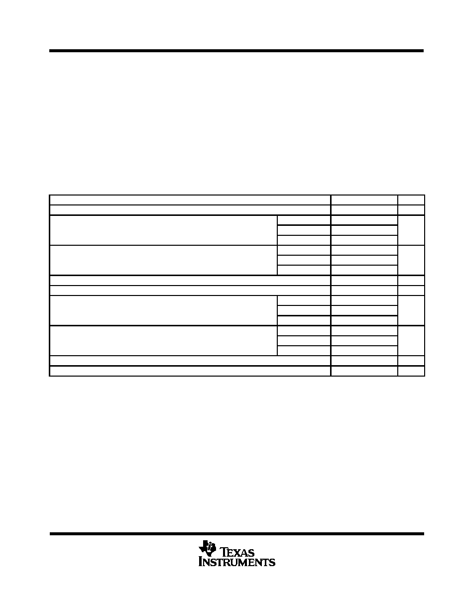
recommended operating conditions
MIN
NOM
MAX
UNIT
VCC
Supply voltage
3
5
5.5
V
VCC = 3 V
2.1
VIH
High-level input voltage
VCC = 4.5 V
3.15
V
VCC = 5.5 V
3.85
VCC = 3 V
0.9
VIL
Low-level input voltage
VCC = 4.5 V
1.35
V
VCC = 5.5 V
1.65
VI
Input voltage
0
VCC
V
VO
Output voltage
0
VCC
V
VCC = 3 V
Ù 4
IOH
High-level output current
VCC = 4.5 V
Ù24
mA
VCC = 5.5 V
Ù24
VCC = 3 V
12
IOL
Low-level output current
VCC = 4.5 V
24
mA
VCC = 5.5 V
24
t/
v
Input transition rise or fall rate
0
10
ns/V
TA
Operating free-air temperature
Ù 40
85
¯
C
74AC11378
HEX DÙTYPE FLIPÙFLOP
WITH CLOCK ENABLE
SCAS150 Ù APRIL 1991 Ù REVISED APRIL 1993
4
POST OFFICE BOX 655303
ñ
DALLAS, TEXAS 75265
POST OFFICE BOX 1443
ñ
HOUSTON, TEXAS 77251Ù1443
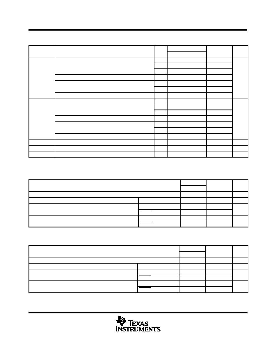
electrical characteristics over recommended operating free-air temperature range (unless
otherwise noted)
PARAMETER
TEST CONDITIONS
VCC
TA = 25
¯
C
MIN
MAX
UNIT
PARAMETER
TEST CONDITIONS
VCC
MIN
TYP
MAX
MIN
MAX
UNIT
3 V
2.9
2.9
IOH = Ù 50
ç
A
4.5 V
4.4
4.4
5.5 V
5.4
5.4
VOH
IOH = Ù 4 mA
3 V
2.58
2.48
V
I
24
A
4.5 V
3.94
3.8
IOL = Ù 24 mA
5.5 V
4.94
4.8
IOH = Ù 75 mA
5.5 V
3.85
3 V
0.1
0.1
IOL = 50
ç
A
4.5 V
0.1
0.1
5.5 V
0.1
0.1
VOL
IOL = 12 mA
3 V
0.36
0.44
V
IOL = 24 mA
4.5 V
0.36
0.44
IOL = 24 mA
5.5 V
0.36
0.44
IOL = 75 mA
5.5 V
1.65
II
VI = VCC or GND
5.5 V
Ý
0.1
Ý
1
ç
A
ICC
VI = VCC or GND,
IO = 0
5.5 V
8
80
ç
A
Ci
VI = VCC or GND
5 V
4
pF
Not more than one output should be tested at a time, and the duration of the test should not exceed 10 ms.
timing requirements over recommended operating free-air temperature range, V
CC
= 3.3 V
Ý
0.3 V
(unless otherwise noted) (see Figure 1)
TA = 25
¯
C
MIN
MAX
UNIT
MIN
MAX
MIN
MAX
UNIT
fclock
Clock frequency
0
90
0
90
MHz
tw
Pulse duration
CLK high or low
5.5
5.5
ns
t
Setup time before CLK
Data
8
8
ns
tsu
Setup time, before CLK
CLKEN high or low
6.5
6.5
ns
th
Hold time after CLK
Data
0
0
ns
th
Hold time, after CLK
CLKEN high or low
0
0
ns
timing requirements over recommended operating free-air temperature range, V
CC
= 5 V
Ý
0.5 V
(unless otherwise noted) (see Figure 1)
TA = 25
¯
C
MIN
MAX
UNIT
MIN
MAX
MIN
MAX
UNIT
fclock
Clock frequency
0
110
0
110
MHz
tw
Pulse duration
CLK high or low
4
4
ns
t
Setup time before CLK
Data
5
5
ns
tsu
Setup time, before CLK
CLKEN high or low
4.5
4.5
ns
th
Hold time after CLK
Data
0
0
ns
th
Hold time, after CLK
CLKEN high or low
0
ns
74AC11378
HEX DÙTYPE FLIPÙFLOP
WITH CLOCK ENABLE
SCAS150 Ù APRIL 1991 Ù REVISED APRIL 1993
5
POST OFFICE BOX 655303
ñ
DALLAS, TEXAS 75265
POST OFFICE BOX 1443
ñ
HOUSTON, TEXAS 77251Ù1443
switching characteristics over recommended operating free-air temperature range,
V
CC
= 3.3 V
Ý
0.3 V (unless otherwise noted) (see Figure 1)
PARAMETER
FROM
TO
TA = 25
¯
C
MIN
MAX
UNIT
PARAMETER
(INPUT)
(OUTPUT)
MIN
TYP
MAX
MIN
MAX
UNIT
fmax
90
115
90
MHz
tPLH
CLK
Any Q
3
7.6
9.5
3
10.9
ns
tPHL
CLK
Any Q
3.6
9.8
12.8
3.6
14
ns
switching characteristics over recommended operating free-air temperature range,
V
CC
= 5 V
Ý
0.5 V (unless otherwise noted) (see Figure 1)
PARAMETER
FROM
TO
TA = 25
¯
C
MIN
MAX
UNIT
PARAMETER
(INPUT)
(OUTPUT)
MIN
TYP
MAX
MIN
MAX
UNIT
fmax
110
140
110
MHz
tPLH
CLK
Any Q
2.4
4.3
7
2.4
7.7
ns
tPHL
CLK
Any Q
3
6.2
8.8
3
9.7
ns
operating characteristics, V
CC
= 5 V, T
A
= 25
¯
C
PARAMETER
TEST CONDITIONS
TYP
UNIT
Cpd
Power dissipation capacitance
CL = 50 pF,
f = 1 MHz
30
pF

74AC11378
HEX DÙTYPE FLIPÙFLOP
WITH CLOCK ENABLE
SCAS150 Ù APRIL 1991 Ù REVISED APRIL 1993
6
POST OFFICE BOX 655303
ñ
DALLAS, TEXAS 75265
POST OFFICE BOX 1443
ñ
HOUSTON, TEXAS 77251Ù1443
From Output
Under Test
500
LOAD CIRCUIT
0 V
0 V
Input
(see Note B)
In-Phase
Output
Out-Of-Phase
Output
tPLH
tPHL
tPHL
tPLH
VOLTAGE WAVEFORMS
PROPAGATION DELAY TIMES
VOH
VOH
VOL
VOL
tw
High-Level
Input
Low-Level
Input
VOLTAGE WAVEFORMS
PULSE DURATIONS
tsu
th
Timing
Input
(see Note B)
Data
Input
VOLTAGE WAVEFORMS
SETUP AND HOLD TIMES
0 V
0 V
VCC
50%
0 V
VCC
VCC
50%
50%
50% VCC
VCC
VCC
CL = 50 pF
(see Note A)
PARAMETER MEASUREMENT INFORMATION
50% VCC
50% VCC
50% VCC
50% VCC
50% VCC
50% VCC
50% VCC
50% VCC
50% VCC
NOTES: A. CL includes probe and jig capacitance.
B. Input pulses are supplied by generators having the following characteristics: PRR
10 MHz, ZO = 50
, tr = 3 ns, tf = 3 ns.
C. The outputs are measured one at a time with one input transition per measurement.
Figure 1. Load Circuit and Voltage Waveforms

IMPORTANT NOTICE
Texas Instruments and its subsidiaries (TI) reserve the right to make changes to their products or to discontinue
any product or service without notice, and advise customers to obtain the latest version of relevant information
to verify, before placing orders, that information being relied on is current and complete. All products are sold
subject to the terms and conditions of sale supplied at the time of order acknowledgement, including those
pertaining to warranty, patent infringement, and limitation of liability.
TI warrants performance of its semiconductor products to the specifications applicable at the time of sale in
accordance with TI's standard warranty. Testing and other quality control techniques are utilized to the extent
TI deems necessary to support this warranty. Specific testing of all parameters of each device is not necessarily
performed, except those mandated by government requirements.
CERTAIN APPLICATIONS USING SEMICONDUCTOR PRODUCTS MAY INVOLVE POTENTIAL RISKS OF
DEATH, PERSONAL INJURY, OR SEVERE PROPERTY OR ENVIRONMENTAL DAMAGE ("CRITICAL
APPLICATIONS"). TI SEMICONDUCTOR PRODUCTS ARE NOT DESIGNED, AUTHORIZED, OR
WARRANTED TO BE SUITABLE FOR USE IN LIFE-SUPPORT DEVICES OR SYSTEMS OR OTHER
CRITICAL APPLICATIONS. INCLUSION OF TI PRODUCTS IN SUCH APPLICATIONS IS UNDERSTOOD TO
BE FULLY AT THE CUSTOMER'S RISK.
In order to minimize risks associated with the customer's applications, adequate design and operating
safeguards must be provided by the customer to minimize inherent or procedural hazards.
TI assumes no liability for applications assistance or customer product design. TI does not warrant or represent
that any license, either express or implied, is granted under any patent right, copyright, mask work right, or other
intellectual property right of TI covering or relating to any combination, machine, or process in which such
semiconductor products or services might be or are used. TI's publication of information regarding any third
party's products or services does not constitute TI's approval, warranty or endorsement thereof.
Copyright
ˋ
1998, Texas Instruments Incorporated