TSL202R
128 y 1 LINEAR SENSOR ARRAY
TAOS032B AUGUST 2002
1
The
LUMENOLOGY
r
Company
t
t
Copyright
E
2002, TAOS Inc.
www.taosinc.com
D
128
×
1 Sensor-Element Organization
D
200 Dots-Per-Inch (DPI) Sensor Pitch
D
High Linearity and Uniformity
D
Wide Dynamic Range . . . 2000:1 (66 dB)
D
Output Referenced to Ground
D
Low Image Lag . . . 0.5% Typ
D
Operation to 5 MHz
D
Single 5-V Supply
D
Replacement for TSL202
Description
The TSL202R linear sensor array consists of two sections of 64 photodiodes and associated charge amplifier
circuitry arranged to form a contiguous 128
×
1 array. The pixels measure 120
µ
m (H) by 70
µ
m (W) with 125-
µ
m
center-to-center spacing and 55-
µ
m spacing between pixels. Operation is simplified by internal control logic that
requires only a serial-input (SI) signal and a clock.
The TSL202R is intended for use in a wide variety of applications including mark detection and code reading,
optical character recognition (OCR) and contact imaging, edge detection and positioning as well as optical linear
and rotary encoding.
Functional Block Diagram (each section -- pin numbers apply to section 1)
2
3
SI
CLK
64-Bit Shift Register
Q64
Switch Control Logic
Integrator
Reset
_
+
Pixel 1
Pixel
2
Pixel
64
Pixel
3
Sample/
Output
Analog
Bus
Q3
Q2
Q1
Output
Amplifier
Gain
Trim
V
DD
AO
GND
5
1
4
R
L
(External
330
W
Load)
t
t
Texas Advanced Optoelectronic Solutions Inc.
800 Jupiter Road, Suite 205
S
Plano, TX 75074
S
(972) 673-0759
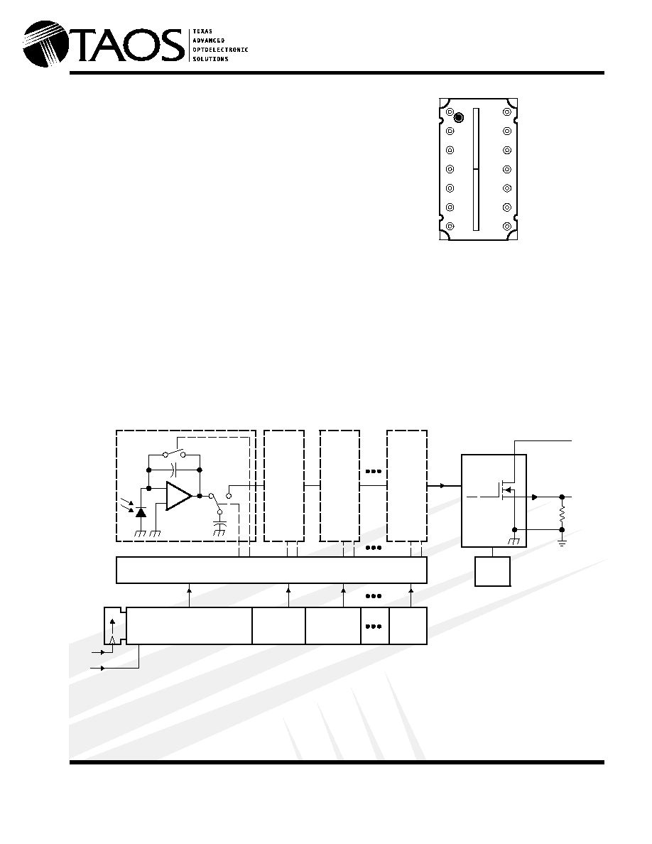
(TOP VIEW)
NC No internal connection
ÉÉ
ÉÉ
ÉÉ
ÉÉ
ÉÉ
ÇÇ
ÇÇ
ÇÇ
ÇÇ
ÇÇ
V
DD
1
SI1 2
CLK 3
AO1 4
GND 5
SO2 6
NC 7
14 NC
13 SO1
12 GND
11 NC
10 SI2
9 NC
8 AO2
TSL202R
128 y 1 LINEAR SENSOR ARRAY
TAOS032B AUGUST 2002
2
t
t
Copyright
E
2002, TAOS Inc.
The
LUMENOLOGY
r
Company
www.taosinc.com
Terminal Functions
TERMINAL
NAME
NO.
DESCRIPTION
AO1
4
Analog output of section 1
AO2
8
Analog output of section 2
CLK
3
Clock. Clk controls charge transfer, pixel output, and reset.
GND
5,12
Ground (substrate). All voltages are referenced to GND.
NC
7, 9, 11, 14
No internal connection
SI1
2
Serial input (section 1). SI1 defines the start of the data-out sequence.
SI2
10
Serial input (section 2). SI2 defines the start of the data-out sequence.
SO1
13
Serial output (section 1). SO1 provides a signal to drive the SI2 input.
SO2
6
Serial output (section 2). SO2 provides a signal to drive the SI input of another device for
cascading or as an end-of-data indication.
V
DD
1
Supply voltage. Supply voltage for both analog and digital circuitry.
Detailed Description
The sensor consists of 128 photodiodes arranged in a linear array. Light energy impinging on a photodiode
generates photocurrent, which is integrated by the active integration circuitry associated with that pixel. During
the integration period, a sampling capacitor connects to the output of the integrator through an analog switch.
The amount of charge accumulated at each pixel is directly proportional to the light intensity and the integration
time. The integration time is the interval between two consecutive output periods.
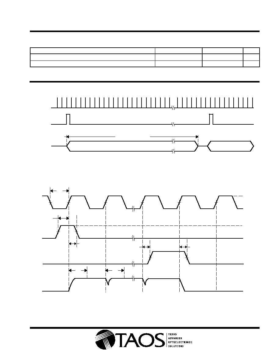
The output and reset of the integrators is controlled by a 128-bit shift register and reset logic. An output cycle
is initiated by clocking in a logic 1 on SI for one positive going clock edge (see Figures1 and 2)
. As the SI pulse
is clocked through the 128-bit shift register, the charge on the sampling capacitor of each pixel is sequentially
connected to a charge-coupled output amplifier that generates a voltage output, AO. When the bit position goes
low, the pixel integrator is reset. On the 129th clock rising edge, the SI pulse is clocked out of the shift register
and the output assumes a high-impedance state. Note that this 129th clock pulse is required to terminate the
output of the 128th pixel and return the internal logic to a known state. A subsequent SI pulse can be presented
as early as the 130th clock pulse, thereby initiating another pixel output cycle.
The voltage developed at analog output (AO) is given by:
V
out
= V
drk
+ (R
e
) (E
e
) (t
int
)
where:
V
out
is the analog output voltage for white condition
V
drk
is the analog output voltage for dark condition
R
e
is the device responsivity for a given wavelength of light given in V/(
µ
J/cm
2
)
E
e
is the incident irradiance in
µ
W/cm
2
t
int
is integration time in seconds
AO is driven by a source follower that requires an external pulldown resistor (330-
typical). The output is
nominally 0 V for no light input, 2 V for normal white-level, and 3.4 V for saturation light level. When the device
is not in the output phase, AO is in a high impedance state.
A 0.1
µ
F bypass capacitor should be connected between V
DD
and ground as close as possible to the device.
For proper operation, after meeting the minimum hold time condition, SI must go low before the next rising edge of the clock.
TSL202R
128 y 1 LINEAR SENSOR ARRAY
TAOS032B AUGUST 2002
3
The
LUMENOLOGY
r
Company
t
t
Copyright
E
2002, TAOS Inc.
www.taosinc.com
Absolute Maximum Ratings
Supply voltage range, V
DD
0.3 V to 6 V
. . . . . . . . . . . . . . . . . . . . . . . . . . . . . . . . . . . . . . . . . . . . . . . . . . . . . . . . . . .
Input voltage range, V
I
0.3 V to V
DD
+ 0.3V
. . . . . . . . . . . . . . . . . . . . . . . . . . . . . . . . . . . . . . . . . . . . . . . . . . . . . . .
Input clamp current, I
IK
(V
I
< 0 or V
I
> V
DD
)
20 mA to 20 mA
. . . . . . . . . . . . . . . . . . . . . . . . . . . . . . . . . . . . . . . .
Output clamp current, I
OK
(V
O
< 0 or V
O
> V
DD
)
25 mA to 25 mA
. . . . . . . . . . . . . . . . . . . . . . . . . . . . . . . . . . . .
Voltage range applied to any output in the high impedance or
power-off state, V
O
0.3 V to V
DD
+ 0.3V
. . . . . . . . . . . . . . . . . . . . . . . . . . . . . . . . . . . . . . . . . . . . . . . . . . .
Continuous output current, I
O
(V
O
= 0 to V
DD
)
25 mA to 25 mA
. . . . . . . . . . . . . . . . . . . . . . . . . . . . . . . . . . . . . .
Continuous current through V
DD
or GND
40 mA to 40 mA
. . . . . . . . . . . . . . . . . . . . . . . . . . . . . . . . . . . . . . . . . .
Analog output current range, I
O
25 mA to 25 mA
. . . . . . . . . . . . . . . . . . . . . . . . . . . . . . . . . . . . . . . . . . . . . . . . . .
Operating free-air temperature range, T
A
25
°
C to 85
°
C
. . . . . . . . . . . . . . . . . . . . . . . . . . . . . . . . . . . . . . . . . . . .
Storage temperature range, T
stg
25
°
C to 85
°
C
. . . . . . . . . . . . . . . . . . . . . . . . . . . . . . . . . . . . . . . . . . . . . . . . . . . .
Lead temperature 1,6 mm (1/16 inch) from case for 10 seconds
260
°
C
. . . . . . . . . . . . . . . . . . . . . . . . . . . . . . .
ESD tolerance, human body model
2000 V
. . . . . . . . . . . . . . . . . . . . . . . . . . . . . . . . . . . . . . . . . . . . . . . . . . . . . . . .
Stresses beyond those listed under "Absolute Maximum Ratings" may cause permanent damage to the device. These are stress ratings only, and
functional operation of the device at these or any other conditions beyond those indicated under "Recommended Operating Conditions" is not
implied. Exposure to absolute-maximum-rated conditions for extended periods may affect device reliability.
Recommended Operating Conditions (see Figure 1 and Figure 2)
MIN
NOM
MAX
UNIT
Supply voltage, V
DD
4.5
5
5.5
V
Input voltage, V
I
0
V
DD
V
High-level input voltage, V
IH
2
V
DD
V
Low-level input voltage, V
IL
0
0.8
V
Wavelength of light source,
400
1000
nm
Clock frequency, f
clock
5
5000
kHz
Sensor integration time, serial, t
int
0.026
100
ms
Sensor integration time, parallel, t
int
0.013
100
ms
Operating free-air temperature, T
A
0
70
°
C
Load resistance, R
L
300
4700
Load capacitance, C
L
420
pF
TSL202R
128 y 1 LINEAR SENSOR ARRAY
TAOS032B AUGUST 2002
4
t
t
Copyright
E
2002, TAOS Inc.
The
LUMENOLOGY
r
Company
www.taosinc.com
Electrical Characteristics at f
clock
= 1 MHz, V
DD
= 5 V, T
A
= 25
°
C,
p
= 640 nm, t
int
= 5 ms,
R
L
= 330
, E
e
= 16.5
µ
W/cm
2
(unless otherwise noted)
PARAMETER
TEST CONDITIONS
MIN
TYP
MAX
UNIT
V
out
Analog output voltage (white, average over 128 pixels)
See Note 1
1.6
2
2.4
V
V
drk
Analog output voltage (dark, average over 128 pixels)
0
50
150
mV
PRNU
Pixel response nonuniformity
See Notes 2 & 3
±
4%
±
10%
Nonlinearity of analog output voltage
See Note 3
±
0.4%
FS
Output noise voltage
See Note 4
1
mVrms
R
e
Responsivity
18
23
30
V/
(µ
J/cm
2
)
SE
Saturation exposure
See Note 5
142
nJ/cm
2
V
sat
Analog output saturation voltage
2.5
3.4
V
DSNU
Dark signal nonuniformity
All pixels
See Note 6
25
120
mV
IL
Image lag
See Note 7
0.5%
I
DD
Supply current, output idle
5
8
mA
I
IH
High-level input current
V
I
= V
DD
10
µ
A
I
IL
Low-level input current
V
I
= 0
10
µ
A
V
OH
High level output voltage SO1 and SO2
I
O
= 50
µ
A
4.5
4.95
V
V
OH
High-level output voltage, SO1 and SO2
I
O
= 4 mA
4.6
V
V
OL
Low level output voltage SO1 and SO2
I
O
= 50
µ
A
0.01
0.1
V
V
OL
Low-level output voltage, SO1 and SO2
I
O
= 4 mA
0.4
V
C
i(SI)
Input capacitance, SI
5
pF
C
i(CLK)
Input capacitance, CLK
10
pF
NOTES: 1. The array is uniformly illuminated with a diffused LED source having a peak wavelength of 640 nm.
2. PRNU is the maximum difference between the voltage from any single pixel and the average output voltage from all pixels of the
device under test when the array is uniformly illuminated at the white irradiance level. PRNU includes DSNU.
3. Nonlinearity is defined as the maximum deviation from a best-fit straight line over the dark-to-white irradiance levels, as a percent
of analog output voltage (white).
4. RMS noise is the standard deviation of a single-pixel output under constant illumination as observed over a 5-second period.
5. Minimum saturation exposure is calculated using the minimum V
sat
, the maximum V
drk
, and the maximum R
e
.
6. DSNU is the difference between the maximum and minimum output voltage in the absence of illumination.
7. Image lag is a residual signal left in a pixel from a previous exposure. It is defined as a percent of white-level signal remaining after
a pixel is exposed to a white condition followed by a dark condition:
IL
+
V
out (IL)
*
V
drk
V
out (white)
*
V
drk
100
Timing Requirements (see Figure 1 and Figure 2)
MIN
NOM
MAX
UNIT
t
su(SI)
Setup time, serial input (see Note 8)
20
ns
t
h(SI)
Hold time, serial input (see Note 8 and Note 9)
0
ns
t
w
Pulse duration, clock high or low
50
ns
t
r
, t
f
Input transition (rise and fall) time
0
500
ns
NOTES: 8. Input pulses have the following characteristics: t
r
= 6 ns, t
f
= 6 ns.
9. SI must go low before the rising edge of the next clock pulse.
TSL202R
128 y 1 LINEAR SENSOR ARRAY
TAOS032B AUGUST 2002
5
The
LUMENOLOGY
r
Company
t
t
Copyright
E
2002, TAOS Inc.
www.taosinc.com
Dynamic Characteristics over recommended ranges of supply voltage and operating free-air
temperature (see Figure 2)
PARAMETER
TEST CONDITIONS
MIN
TYP
MAX
UNIT
t
s
Analog output settling time to
±
1%
R
L
= 330
,
C
L
= 10 pF
185
ns
t
pd(SO)
Propagation delay time, SO1, SO2
50
ns
TYPICAL CHARACTERISTICS
ÎÎÎÎÎÎÎÎÎÎÎÎÎÎÎÎÎÎÎÎ
ÎÎÎÎÎÎÎÎÎÎÎÎÎÎÎÎÎÎÎÎ
ÎÎÎÎÎÎÎÎÎÎÎÎÎÎÎÎÎÎÎÎ
ÎÎÎÎÎÎÎ
ÎÎÎÎÎÎÎ
ÎÎÎÎÎÎÎ
129 Clock Cycles
CLK
SI
AO
Hi-Z
Hi-Z
Figure 1. Timing Waveforms
AO1 (A02)
SI1 (SI2)
CLK
Pixel 64 (128)
t
s
0 V
0 V
5 V
2.5 V
t
h(SI)
5 V
t
su(SI)
t
w
1 (65)
2 (66)
64 (128)
65 (129)
t
s
Pixel 1 (65)
2.5 V
2.5 V
2.5 V
2.5 V
t
pd(SO)
t
pd(SO)
SO1 (SO2)
Figure 2. Operational Waveforms (each section)