July 2003
1/16
®
VNQ660SP
QUAD CHANNEL HIGH SIDE SOLID STATE RELAY
(*) Per each channel
s
OUTPUT CURRENT PER CHANNEL: 6A
s
CMOS COMPATIBLE INPUTS
s
OPEN LOAD DETECTION (OFF STATE)
s
UNDERVOLTAGE & OVERVOLTAGE
n
SHUT- DOWN
s
OVERVOLTAGE CLAMP
s
THERMAL SHUT-DOWN
s
CURRENT LIMITATION
s
VERY LOW STAND-BY POWER DISSIPATION
s
PROTECTION AGAINST:
n
LOSS OF GROUND & LOSS OF V
CC
s
REVERSE BATTERY PROTECTION (**)
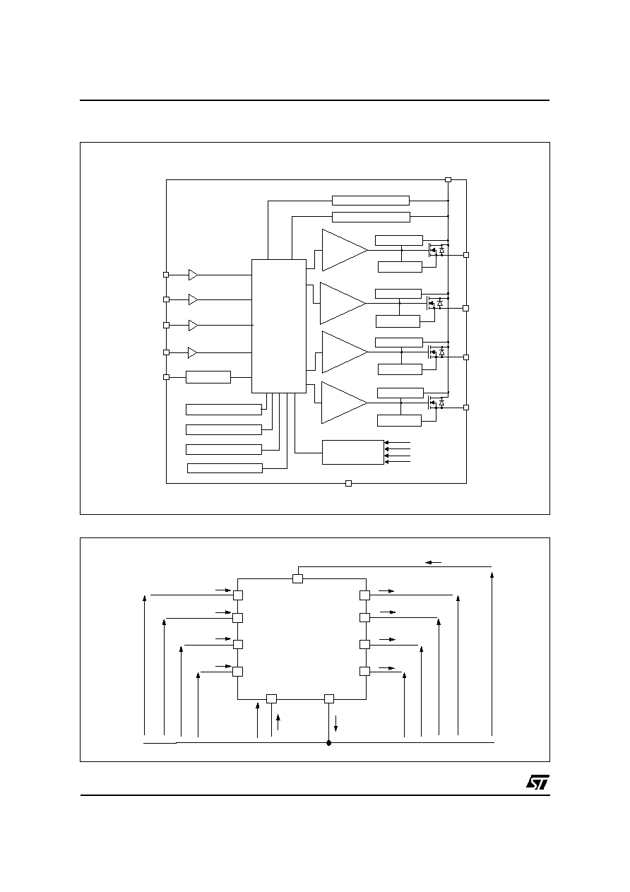
DESCRIPTION
The VNQ660SP is a monolithic device made by
using
|
STMicroelectronics VIPower M0-3
Technology, intended for driving resistive or
inductive loads with one side connected to ground.
This device has four independent channels. Built-
in thermal shut down and output current limitation
protect the chip from over temperature and short
circuit.
TYPE
R
DS(on)
I
OUT
V
CC
VNQ660SP
50m
(*)
6A
36 V
ABSOLUTE MAXIMUM RATING
(**) See application schematic at page 8
Symbol
Parameter
Value
Unit
V
CC
Supply voltage (continuous)
41
V
-V
CC
Reverse supply voltage (continuous)
-0.3
V
I
OUT
Output current (continuous), per each channel
Internally limited
A
I
R
Reverse output current (continuous), per each channel
-15
A
I
IN
Input current
+/- 10
mA
I
STAT
Status current
+/- 10
mA
I
GND
Ground current at T
C
<25
°
C (continuous)
-200
mA
V
ESD
Electrostatic Discharge (Human Body Model: R=1.5K
;
C=100pF)
- INPUT
- STATUS
- OUTPUT
- V
CC
4000
4000
5000
5000
V
V
V
V
P
tot
Power dissipation at T
C
=25
°
C
113.6
W
T
j
Junction operating temperature
-40 to 150
°
C
T
stg
Storage temperature
-65 to 150
°
C
E
C
Non repetitive clamping energy at T
C
=25
°
C
150
mJ
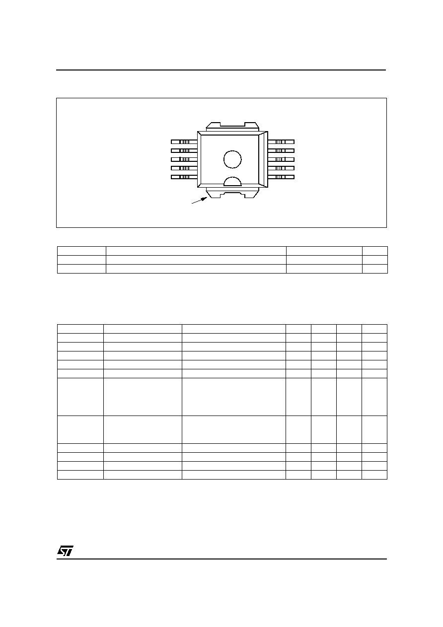
PowerSO-10
TM
1
10
ORDER CODES
PACKAGE
TUBE
T&R
PowerSO-10
TM
VNQ660SP
VNQ660SP13TR
3/16
VNQ660SP
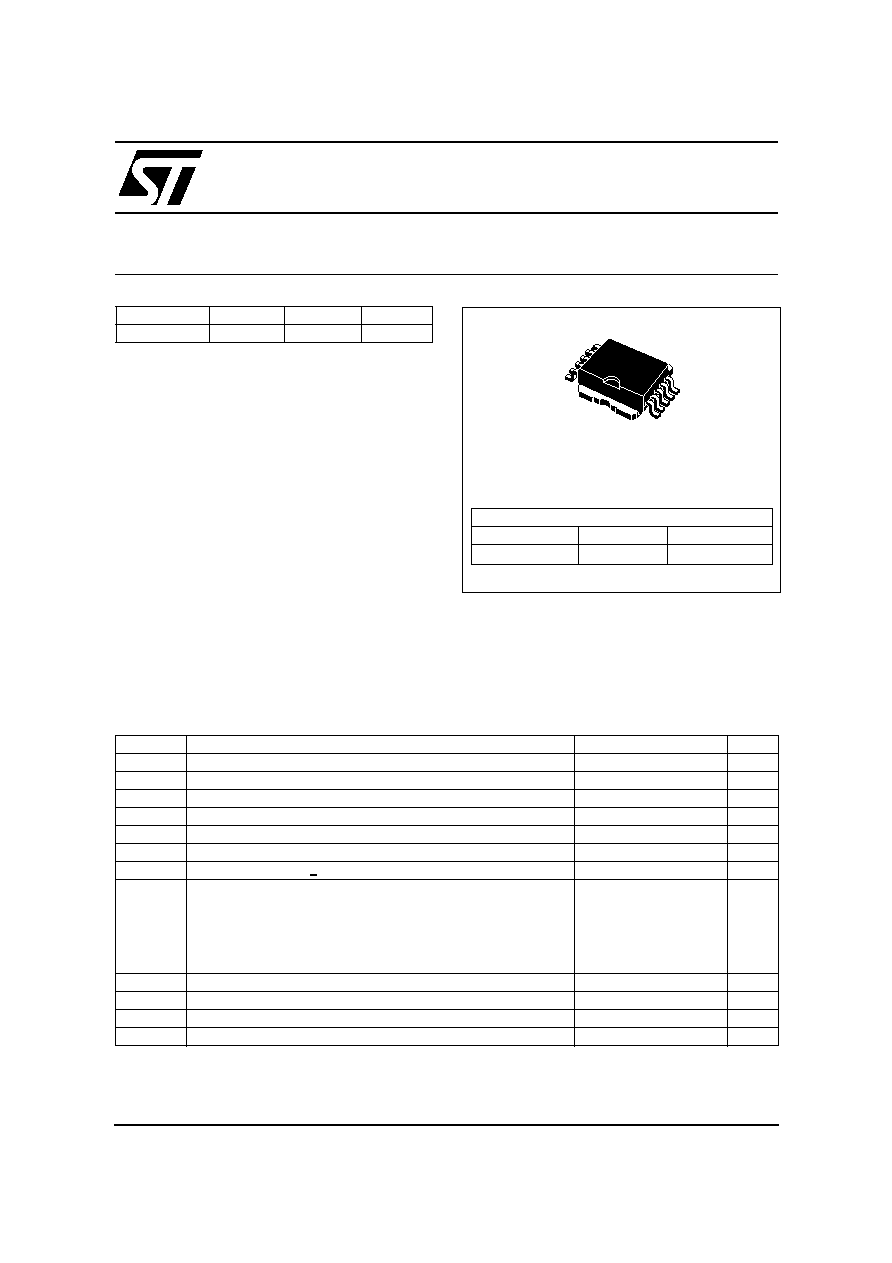
CONNECTION DIAGRAM (TOP VIEW)
1
2
3
4
5
6
7
8
9
10
11
GND
OUTPUT 4
OUTPUT 3
OUTPUT 2
OUTPUT 1
STATUS
INPUT 4
INPUT 3
INPUT 2
INPUT 1
V
CC
THERMAL DATA
(*) When mounted on a standard single-sided FR-4 board with 0.5cm˛ of Cu (at least 35
µ
m thick). Horizontal mounting and no artificial air
flow.
ELECTRICAL CHARACTERISTICS (V
CC
=6V up to 24V; -40
°
C<T
j
<150
°
C unless otherwise specified)
POWER (per each channel)
(**) Per device.
Symbol
Parameter
Value
Unit
R
thj-case
Thermal resistance junction-case (MAX) (all channels on)
1.1
°
C/W
R
thj-amb
Thermal resistance junction-ambient (MAX)
51.1 (*)
°
C/W
Symbol
Parameter
Test Conditions
Min
Typ
Max
Unit
V
CC
(**)
Operating supply voltage
6
13
36
V
V
USD
(**)
Undervoltage shutdown
3.5
4.6
6
V
V
UVhyst
(**)
Undervoltage hysteresis
0.2
1
V
V
OV
(**)
Overvoltage shutdown
36
V
V
OVhyst
(**)
Overvoltage hysteresis
0.25
V
I
S
(**)
Supply current
Off state; Input=0V; V
CC
=13.5V
Off state; Input=0V; V
CC
=13.5V
T
j
=25
°
C
On state Input=3.25V; 9V<V
CC
<18V
12
12
6
40
25
12
µ
A
µ
A
mA
R
DS(on)
On state resistance
I
OUT
=1A; T
j
=25
°
C; 9V<V
CC
<18V
I
OUT
=1A, T
j
=150
°
C; 9V<V
CC
<18V
I
OUT
=1A; V
CC
=6V
40
85
50
100
130
m
m
m
I
L(off1)
Off state output current
V
IN
=V
OUT
=0V
0
50
µ
A
I
L(off2)
Off State Output Current
V
IN
=0V; V
OUT
=3.5V
-75
0
µ
A
I
L(off3)
Off State Output Current
V
IN
=V
OUT
=0V; V
CC
=13V; T
j
=125°C
5
µ
A
I
L(off4)
Off State Output Current
V
IN
=V
OUT
=0V; V
CC
=13V; T
j
=25°C
3
µ
A
4/16
VNQ660SP
ELECTRICAL CHARACTERISTICS (continued)
SWITCHING (V
CC
=13V)
PROTECTIONS (per each channel)
LOGIC INPUT (per each channel)
OPENLOAD DETECTION (off state) per each channel
(*) See Figure 1
Symbol
Parameter
Test Conditions
Min
Typ
Max
Unit
t
d(on)
Turn-on delay time
R
L
=13
channels 1,2,3,4
40
70
µ
s
t
d(off)
Turn-on delay time
R
L
=13
channels 1,2,3,4
40
140
µ
s
dV
OUT
/dt
(on)
Turn-on voltage slope
R
L
=13
channels 1,2,3,4
See
relative
diagram
V
/µ
s
dV
OUT
/dt
(off)
Turn-off voltage slope
R
L
=13
channels 1,2,3,4
See
relative
diagram
V
/µ
s
Symbol
Parameter
Test Conditions
Min
Typ
Max
Unit
T
TSD
Shutdown temperature
150
170
200
°
C
T
R
Reset temperature
135
°
C
T
hyst
Thermal hysteresis
7
15
25
°
C
I
lim
DC Short circuit current
9V<V
CC
<36V
6V<V
CC
<36V
6
10
18
18
A
A
V
demag
Turn-off output voltage
clamp
I
OUT
=2A; V
IN
=0V; L=6mH
V
CC
-41 V
CC
-48 V
CC
-55
V
V
STAT
Status low output
voltage
I
STAT
=1.6mA
0.5
V
I
LSTAT
Status leakage current
Normal operation; V
STAT
=5V
10
µ
A
C
STAT
Status pin input
capacitance
Normal operation; V
STAT
=5V
25
pF
V
SCL
Status clamp voltage
I
STAT
=1mA
I
STAT
=-1mA
6
6.8
-0.7
8
V
V
Symbol
Parameter
Test Conditions
Min
Typ
Max
Unit
V
IL
Input Low Level Voltage
1.25
V
V
IH
Input High Level Voltage
3.25
V
V
HYST
Input Hysteresis Voltage
0.5
V
I
IH
Input high level voltage
V
IN
=3.25V
10
µ
A
I
IL
Input Current
V
IN
=1.25V
1
µ
A
C
IN
Input Capacitance
40
pF
V
ICL
Input Clamp Voltage
I
IN
=1mA
I
IN
=-1mA
6
6.8
-0.7
8
V
V
Symbol
Parameter
Test Conditions
Min
Typ
Max
Unit
t
SDL
Status Delay
(*)
20
µ
s
V
OL
Openload Voltage
Detection Threshold
V
IN
=0V
1.5
2.5
3.5
V
T
DOL
Openload Detection Delay
at Turn Off
V
CC
=18V (*)
300
µ
s
5/16
VNQ660SP
ELECTRICAL TRANSIENT REQUIREMENTS
SWITCHING CHARACTERISTICS
ISO T/R 7637/1
Test Pulse
TEST LEVELS
I
II
III
IV
Delays and
Impedance
1
-25 V
-50 V
-75 V
-100 V
2 ms 10
2
+25 V
+50 V
+75 V
+100 V
0.2 ms 10
3a
-25 V
-50 V
-100 V
-150 V
0.1
µ
s 50
3b
+25 V
+50 V
+75 V
+100 V
0.1
µ
s 50
4
-4 V
-5 V
-6 V
-7 V
100 ms, 0.01
ISO T/R
7637/1
Test Pulse
Test Levels Result
I
II
III
IV
1
C
C
C
C
2
C
C
C
C
3a
C
C
C
C
3b
C
C
C
C
4
C
C
C
C
5
C
E
E
E
Class
Contents
C
All functions of the device are performed as designed after exposure to disturbance.
E
One or more functions of the device is not performed as designed after exposure and cannot be
returned to proper operation without replacing the device.
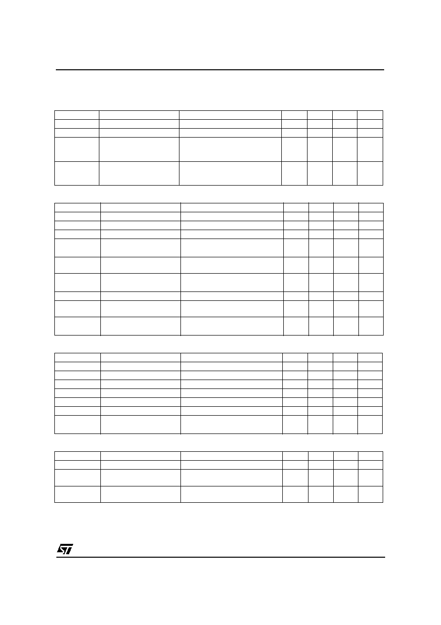
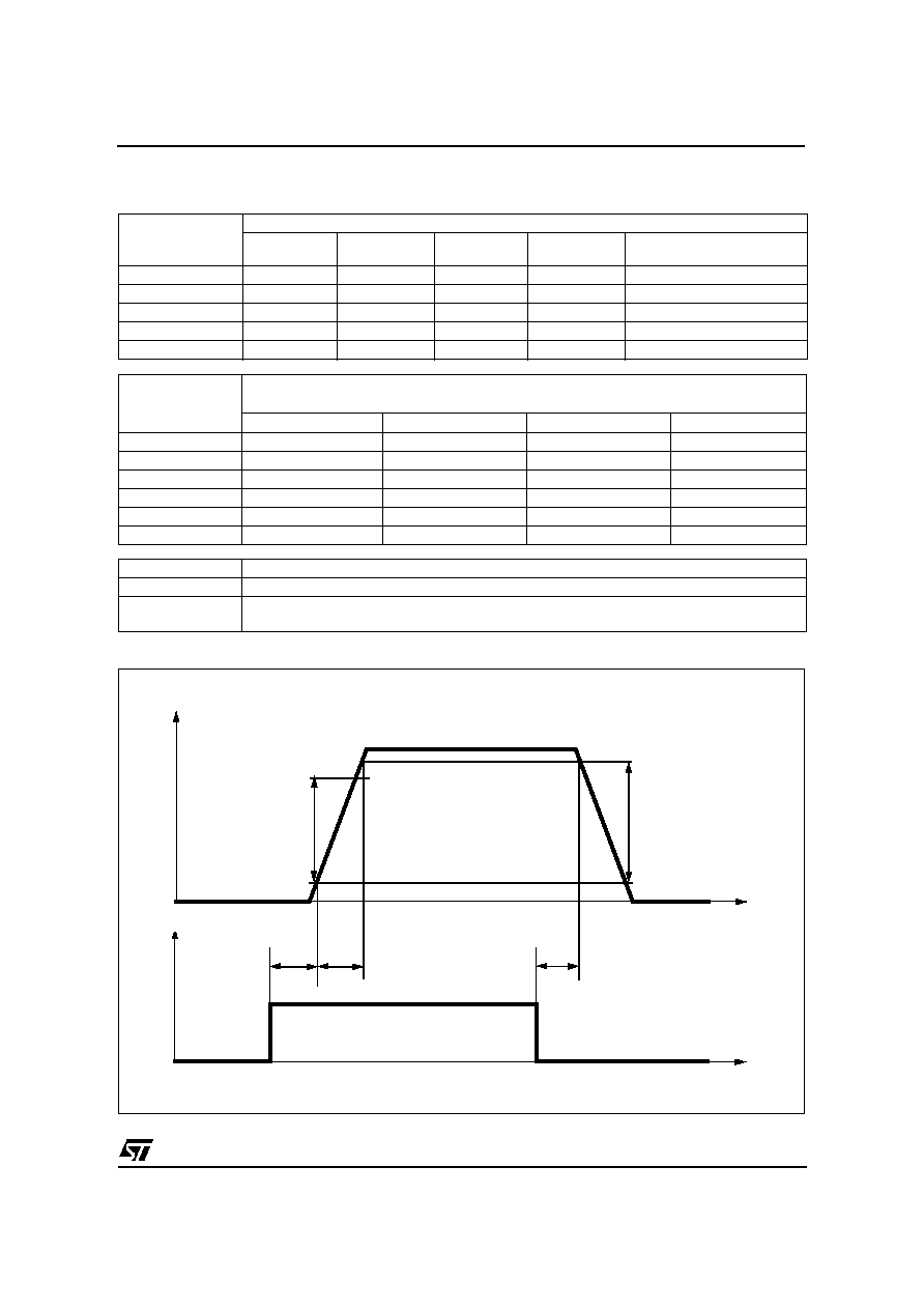
1
t
t
V
LOAD
V
IN
80%
10%
dV
OUT
/dt
(on)
t
d(off)
90%
dV
OUT
/dt
(off)
t
d(on)
t
r