1/18
September 2004
VNH3ASP30-E
AUTOMOTIVE FULLY INTEGRATED
H-BRIDGE MOTOR DRIVER
Rev. 1
Table 1. General Features
s
OUTPUT CURRENT: 30A
s
5V LOGIC LEVEL COMPATIBLE INPUTS
s
UNDERVOLTAGE AND OVERVOLTAGE
SHUT-DOWN
s
OVERVOLTAGE CLAMP
s
THERMAL SHUT DOWN
s
CROSS-CONDUCTION PROTECTION
s
LINEAR CURRENT LIMITER
s
VERY LOW STAND-BY POWER
CONSUMPTION
s
PWM OPERATION UP TO 20 KHz
s
PROTECTION AGAINST:
LOSS OF GROUND AND LOSS OF V
CC
s
CURRENT SENSE OUTPUT PROPORTIONAL
TO MOTOR CURRENT
s
IN COMPLIANCE WITH THE 2002/95/EC
EUROPEAN DIRECTIVE
DESCRIPTION
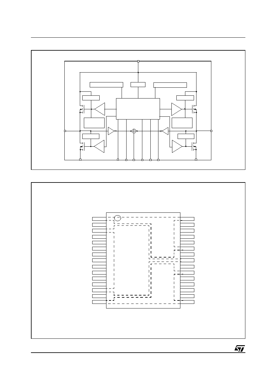
The VNH3ASP30-E is a full bridge motor driver
intended for a wide range of automotive
applications. The device incorporates a dual
monolithic High-Side drivers and two Low-Side
switches. The High-Side driver switch is designed
using STMicroelectronic's well known and proven
proprietary VIPower
TM
M0 technology that allows
to efficiently integrate on the same die a true
Power MOSFET with an intelligent signal/
protection circuitry.
Figure 1. Package
The Low-Side switches are vertical MOSFETs
manufactured using STMicroelectronic's
proprietary EHD (`STripFETTM') process. The
three dice are assembled in MultiPowerSO-30
package on electrically isolated leadframes. This
package, specifically designed for the harsh
automotive environment offers improved thermal
performance thanks to exposed die pads.
Moreover, its fully symmetrical mechanical design
allows superior manufacturability at board level.
The input signals IN
A
and IN
B
can directly
interface to the microcontroller to select the motor
direction and the brake condition. The DIAG
A
/EN
A
or DIAG
B
/EN
B
, when connected to an external
pull-up resistor, enable one leg of the bridge. They
also provide a feedback digital diagnostic signal.
The normal condition operation is explained in the
truth table on page 7. The CS pin allows to monitor
the motor current by delivering a current
proportional to its value. The PWM, up to 20KHz,
lets us to control the speed of the motor in all
possible conditions. In all cases, a low level state
on the PWM pin will turn off both the LS
A
and LS
B
switches. When PWM rises to a high level, LS
A
or
LS
B
turn on again depending on the input pin
state.
Table 2. Order Codes
TYPE
R
DS(on)
I
OUT
V
ccmax
VNH3ASP30-E
42 m
max
(
per leg)
30 A
41 V
MultiPowerSO-30
Package
Tube
Tape and Reel
MultiPowerSO-30
VNH3ASP30-E
VNH3ASP30TR-E
TARGET SPECIFICATION
VNH3ASP30-E
2/18
Figure 2. Block Diagram
Figure 3. Configuration Diagram (Top View)
LOGIC
V
CC
OUT
A
DIAG
A
/EN
A
IN
B
IN
A
GND
A
CS
DIAG
B
/EN
B
LS
A
CLAMP HS
A
LS
A
HS
A
OVERTEMPERATURE A
OVERTEMPERATURE B
O
V
+ U
V
CURRENT
LIMITATION A
OUT
B
GND
B
LS
B
HS
B
CURRENT
LIMITATION B
DRIVER
HS
A
DRIVER
LS
B
DRIVER
HS
B
DRIVER
CLAMP HS
B
CLAMP LS
B
CLAMP LS
A
PWM
1/K
1/K
OUT
A
OUT
A
OUT
A
OUT
B
OUT
B
Nc
V
CC
Nc
IN
A
EN
A
/DIAG
A
Nc
PWM
CS
EN
B
/DIAG
B
IN
B
Nc
Nc
V
CC
OUT
B
Nc
Nc
GND
A
GND
A
GND
A
Nc
V
CC
Nc
GND
B
GND
B
GND
B
1
15
16
30
V
CC
Heat Slug1
OUT
B
Heat Slug2
OUT
A
Heat Slug3
3/18
VNH3ASP30-E
Table 3. Pin Definitions And Functions
Note: (*) GND
A
and GND
B
must be externally connected together.
Table 4. Pin Functions Description
Table 5. Block Descriptions (see Block Diagram)
Pin No
Symbol
Function
1, 25, 30
OUT
A,
Heat Slug2 Source of High-Side Switch A / Drain of Low-Side Switch A
2,4,7,12,14,17, 22, 24,29 NC
Not connected
3, 13, 23
VCC, Heat Slug1
Drain of High-Side Switches and Power Supply Voltage
6
EN
A
/DIAG
A
Status of High-Side and Low-Side Switches A; Open Drain Output
5
IN
A
Clockwise Input
8
PWM
PWM Input
9
CS
Output of Current sense
11
IN
B
Counter Clockwise Input
10
EN
B
/DIAG
B
Status of High-Side and Low-Side Switches B; Open Drain Output
15, 16, 21
OUT
B,
Heat Slug3 Source of High-Side Switch B / Drain of Low-Side Switch B
26, 27, 28
GND
A
Source of Low-Side Switch A (*)
18, 19, 20
GND
B
Source of Low-Side Switch B (*)
Name
Description
V
CC
Battery connection.
GND
A
GND
B
Power grounds, must always be externally connected together.
OUT
A
OUT
B
Power connections to the motor.
IN
A
IN
B
Voltage controlled input pins with hysteresis, CMOS compatible. These two pins control the state of
the bridge in normal operation according to the truth table (brake to V
CC
, Brake to GND, clockwise and
counterclockwise).
PWM
Voltage controlled input pin with hysteresis, CMOS compatible.Gates of Low-Side FETS get
modulated by the PWM signal during their ON phase allowing speed control of the motor
EN
A
/DIAG
A
EN
B
/DIAG
B
Open drain bidirectional logic pins.These pins must be connected to an external pull up resistor. When
externally pulled low, they disable half-bridge A or B. In case of fault detection (thermal shutdown of
a High-Side FET or excessive ON state voltage drop across a Low-Side FET), these pins are pulled
low by the device (see truth table in fault condition).
CS
Analog current sense output. This output sources a current proportional to the motor current. The
information can be read back as an analog voltage across an external resistor.
Name
Description
LOGIC CONTROL
Allows the turn-on and the turn-off of the High Side and the Low Side
switches according to the truth table.
OVERVOLTAGE + UNDERVOLTAGE
Shut-down the device outside the range [5.5V..16V] for the battery
voltage.
HIGH SIDE AND LOW SIDE CLAMP
VOLTAGE
Protect the High Side and the Low Side switches from the high voltage
on the battery line in all configuration for the motor.
HIGH SIDE AND LOW SIDE DRIVER
Drive the gate of the concerned switch to allow a proper R
DS(on)
for the
leg of the bridge.
LINEAR CURRENT LIMITER
Limits the motor current, by reducing the High Side Switch gate-source
voltage when short-circuit to ground occurs.
OVERTEMPERATURE PROTECTION
In case of short-circuit with the increase of the junction's temperature,
shuts-down the concerned High Side to prevent its degradation and to
protect the die.
FAULT DETECTION
Signalize an abnormal behavior of the switches in the half-bridge A or
B by pulling low the concerned ENx/DIAGx pin.
VNH3ASP30-E
4/18
Table 6. Absolute Maximum Rating
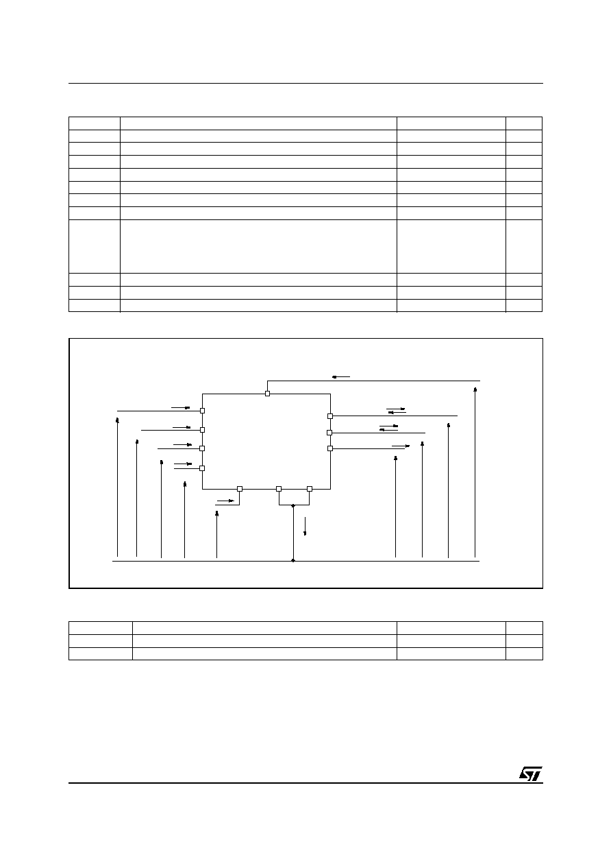
Figure 4. Current and Voltage Conventions
Table 7. Thermal Data
Note: (*) When mounted using the recommended pad size on FR-4 board (see MultiPowerSO-30 Mechanical data).
Symbol
Parameter
Value
Unit
V
CC
Supply Voltage
+ 41
V
I
max
Maximum Output Current (continuous)
30
A
I
R
Reverse Output Current (continuous)
-30
A
I
IN
Input Current (IN
A
and IN
B
pins)
+/- 10
mA
I
EN
Enable Input Current (DIAG
A
/EN
A
and DIAG
B
/EN
B
pins)
+/- 10
mA
I
pw
PWM Input Current
+/- 10
mA
V
CS
Current Sense Maximum Voltage
-3/+15
V
V
ESD
Electrostatic Discharge (R=1.5k
, C=100pF)
- CS pin
- logic pins
- output pins: OUT
A
, OUT
B
, V
CC
2
4
5
kV
kV
kV
T
j
Junction Operating Temperature
Internally Limited
°C
T
c
Case Operating Temperature
-40 to 150
°C
T
STG
Storage Temperature
-55 to 150
°C
Symbol
Parameter
Value
Unit
R
thj-case
Thermal resistance junction-case (Per leg)
(MAX)
1.0
°C/W
R
thj-amb
(*)
Thermal resistance junction-ambient
(MAX)
20
°C/W
V
CC
IN
A
GND
B
I
S
I
OUTA
I
INA
V
INA
V
CC
V
OUTA
I
SENSE
V
OUTB
DIAG
A
/EN
A
I
ENA
I
GND
I
OUTB
IN
B
I
INB
DIAG
B
/EN
B
I
ENB
V
ENB
V
ENA
V
INB
V
SENSE
OUT
A
OUT
B
PWM
CS
I
pw
V
pw
GND
A
GND

5/18
VNH3ASP30-E
ELECTRICAL CHARACTERISTICS
(V
CC
=9V up to 16V; -40
°
C<T
j
<150
°
C; unless otherwise specified)
Table 8. Power
Table 9. Logic Inputs (IN
A
, IN
B
, EN
A
, EN
B
)
Symbol
Parameter
Test Conditions
Min
Typ
Max
Unit
V
CC
Operating supply voltage
5.5
16
V
I
S
Supply Current
Off state:
IN
A
=IN
B
=PWM=0;
T
j
=25
°
C;
V
CC
=13V
IN
A
=IN
B
=PWM=0
12
30
TBD
µ
A
µ
A
On state:
IN
A
or IN
B
=5V, no PWM
IN
A
or IN
B
=5V; PWM=20kHz
10
TBD
mA
mA
R
ONHS
Static High-Side resistance
I
OUT
=12A; T
j
=25°C
I
OUT
=12A; T
j
= - 40
to
150°C
30
60
m
m
R
ONLS
Static Low-Side resistance
I
OUT
=12A; T
j
=25°C
I
OUT
=12A; T
j
= - 40
to
150°C
12
24
m
m
V
f
High Side Free-wheeling
Diode Forward Voltage
I
f
=12A
0.8
1.1
V
I
L(off)
High Side Off State Output
Current (per channel)
T
j
=25°C; V
OUTX
=EN
X
=0V;
V
CC
=13V
T
j
=125°C; V
OUTX
=EN
X
=0V;
V
CC
=13V
3
5
µ
A
µ
A
I
RM
Dynamic Cross-conduction
Current
I
OUT
=12A (see fig. 9)
1.7
A
Symbol
Parameter
Test Conditions
Min
Typ
Max
Unit
V
IL
Input Low Level Voltage
Normal operation (DIAG
X
/EN
X
pin acts as an input pin)
1.25
V
V
IH
Input High Level Voltage
Normal operation (DIAG
X
/EN
X
pin acts as an input pin)
3.25
V
V
IHYST
Input Hysteresis Voltage
Normal operation (DIAG
X
/EN
X
pin acts as an input pin)
0.5
V
V
ICL
Input Clamp Voltage
I
IN
=1mA
I
IN
=-1mA
5.5
-1.0
6.3
-0.7
7.5
-0.3
V
V
I
INL
Input Current
V
IN
=1.25 V
1
µ
A
I
INH
Input Current
V
IN
=3.25 V
10
µ
A
V
DIAG
Enable Output Low Level
Voltage
Fault operation (DIAG
X
/EN
X
pin
acts as an output pin); I
EN
=1mA
0.4
V