1/20
October 2004
VND810-E
DOUBLE CHANNEL HIGH SIDE DRIVER
Rev. 1
Table 1. General Features
(*)
Per each channel
s
CMOS COMPATIBLE INPUTS
s
OPEN DRAIN STATUS OUTPUTS
s
ON STATE OPEN LOAD DETECTION
s
OFF STATE OPEN LOAD DETECTION
s
SHORTED LOAD PROTECTION
s
UNDERVOLTAGE AND OVERVOLTAGE
SHUTDOWN
s
PROTECTION
AGAINST
LOSS OF GROUND
s
VERY LOW STAND-BY CURRENT
s
REVERSE BATTERY PROTECTION (**)
s
IN COMPLIANCE WITH THE 2002/95/EC
EUROPEAN DIRECTIVE
DESCRIPTION
The VND810-E is a monolithic device designed in
STMicroelectronics VIPower M0-3 Technology,
intended for driving any kind of load with one side
connected to ground.
Active V
CC
pin voltage clamp protects the device
against low energy spikes (see ISO7637 transient
compatibility table).
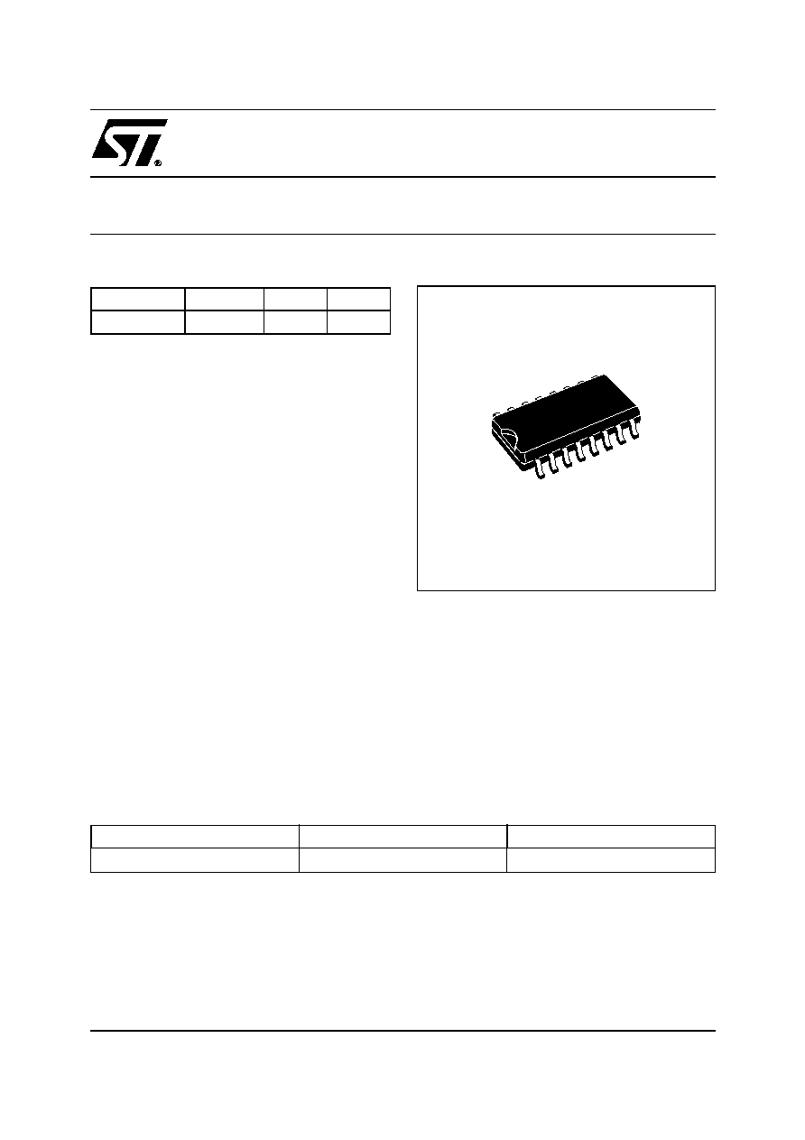
Figure 1. Package
Active current limitation combined with thermal
shutdown and automatic restart protects the
device against overload. The device detects open
load condition both in on and off state. Output
shorted to V
CC
is detected in the off state. Device
automatically turns off in case of ground pin
disconnection.
Table 2. Order Codes
Note: (**) See application schematic at page 9
Type
R
DS(on)
I
out
V
CC
VND810-E
160 m
(*)
3.5A (*)
36 V
SO-16
Package
Tube
Tape and Reel
SO-16
VND810-E
VND810TR-E

VND810-E
2/20
Figure 2. Block Diagram
Table 3. Absolute Maximum Ratings
Symbol
Parameter
Value
Unit
V
CC
DC Supply Voltage
41
V
- V
CC
Reverse DC Supply Voltage
- 0.3
V
- I
GND
DC Reverse Ground Pin Current
- 200
mA
I
OUT
DC Output Current
Internally Limited
A
- I
OUT
Reverse DC Output Current
- 6
A
I
IN
DC Input Current
+/- 10
mA
I
stat
DC Status Current
+/- 10
mA
V
ESD
Electrostatic Discharge (Human Body Model:
R=1.5K
;
C=100pF)
- INPUT
- STATUS
- OUTPUT
- V
CC
4000
4000
5000
5000
V
V
V
V
E
MAX
Maximum Switching Energy
(L=1.5mH; R
L
=0
; V
bat
=13.5V; T
jstart
=150şC;
I
L
=5A)
26
mJ
P
tot
Power Dissipation T
C
=25°C
8.3
W
T
j
Junction Operating Temperature
Internally Limited
°C
T
c
Case Operating Temperature
- 40 to 150
°C
T
stg
Storage Temperature
- 55 to 150
°C
OVERTEMP. 1
V
cc
GND
INPUT1
OUTPUT1
OVERVOLTAGE
LOGIC
DRIVER 1
STATUS1
V
cc
CLAMP
UNDERVOLTAGE
CLAMP 1
OPENLOAD ON 1
CURRENT LIMITER 1
OPENLOAD OFF 1
OUTPUT2
DRIVER 2
CLAMP 2
OPENLOAD ON 2
OPENLOAD OFF 2
OVERTEMP. 2
INPUT2
STATUS2
CURRENT LIMITER 2

3/20
VND810-E
Figure 3. Configuration Diagram (Top View) & Suggested Connections for Unused and N.C. Pins
Figure 4. Current and Voltage Conventions
Table 4. Thermal Data
Note: 1. When mounted on a standard single-sided FR-4 board with 0.5cm
2
of Cu (at least 35
µ
m thick) connected to all V
CC
pins. Horizontal
mounting and no artificial air flow.
Note: 2. When mounted on a standard single-sided FR-4 board with 4cm
2
of Cu (at least 35
µ
m thick) connected to all V
CC
pins. Horizontal
mounting and no artificial air flow.
Symbol
Parameter
Value
Unit
R
thj-lead
Thermal Resistance Junction-lead
15
°C/W
R
thj-amb
Thermal Resistance Junction-ambient
77
(1)
57
(2)
°C/W
Connection / Pin Status
N.C.
Output
Input
Floating
X
X
X
X
To Ground
X
Through 10K
resistor
V
CC
V
CC
OUTPUT 2
OUTPUT 2
OUTPUT 1
V
CC
OUTPUT 1
V
CC
V
CC
INPUT 2
STATUS 2
STATUS 1
INPUT 1
V
CC
GND
N.C.
1
8
9
16
(*) V
Fn
= V
CCn
- V
OUTn
during reverse battery condition
I
S
I
GND
OUTPUT 2
V
CC
GND
STATUS 2
INPUT 2
I
OUT2
I
IN2
I
STAT2
V
STAT2
V
IN2
V
CC
V
OUT2
OUTPUT 1
I
OUT1
V
OUT1
INPUT 1
I
IN1
STATUS 1
I
STAT1
V
IN1
V
STAT1
V
F1
(*)
VND810-E
4/20
ELECTRICAL CHARACTERISTICS
(8V<V
CC
<36V; -40°C < T
j
<150°C, unless otherwise specified)
(Per each channel)
Table 5. Power Output
Note: (**) Per device.
Table 6. Protection (see note 1)
Note: 1. To ensure long term reliability under heavy overload or short circuit conditions, protection and related diagnostic signals must be
used together with a proper software strategy. If the device is subjected to abnormal conditions, this software must limit the duration
and number of activation cycles
Table 7. V
CC
- Output Diode
Symbol
Parameter
Test Conditions
Min.
Typ.
Max.
Unit
V
CC
(**)
Operating Supply Voltage
5.5
13
36
V
V
USD
(**)
Undervoltage Shut-down
3
4
5.5
V
V
OV
(**)
Overvoltage Shut-down
36
V
R
ON
On State Resistance
I
OUT
=1A; T
j
=25°C
I
OUT
=1A; V
CC
>8V
160
320
m
m
I
S
(**)
Supply Current
Off State; V
CC
=13V; V
IN
=V
OUT
=0V
Off State; V
CC
=13V; V
IN
=V
OUT
=0V;
T
j
=25
°C
On State; V
CC
=13V; V
IN
=5V; I
OUT
=0A
12
12
5
40
25
7
µ
A
µ
A
mA
I
L(off1)
Off State Output Current
V
IN
=V
OUT
=0V
0
50
µ
A
I
L(off2)
Off State Output Current
V
IN
=0V; V
OUT
=3.5V
-75
0
µ
A
I
L(off3)
Off State Output Current
V
IN
=V
OUT
=0V; V
CC
=13V; T
j
=125°C
5
µ
A
I
L(off4)
Off State Output Current
V
IN
=V
OUT
=0V; V
CC
=13V; T
j
=25°C
3
µ
A
Symbol
Parameter
Test Conditions
Min.
Typ.
Max.
Unit
T
TSD
Shut-down Temperature
150
175
200
°C
T
R
Reset Temperature
135
°C
T
hyst
Thermal Hysteresis
7
15
°C
t
SDL
Status Delay in Overload
Conditions
T
j
>T
TSD
20
µ
s
I
lim
Current limitation
5.5V<V
CC
<36V
3.5
5
7.5
7.5
A
A
V
demag
Turn-off Output Clamp
Voltage
I
OUT
=1A; L=6mH
V
CC
-
41
V
CC
-48
V
CC
-
55
V
Symbol
Parameter
Test Conditions
Min
Typ
Max
Unit
V
F
Forward on Voltage
-I
OUT
=0.5A; T
j
=150°C
0.6
V

5/20
VND810-E
ELECTRICAL CHARACTERISTICS (continued)
Table 8. Status Pin
Table 9. Switching (V
CC
=13V)
Table 10. Openload Detection
Table 11. Logic Input
Symbol
Parameter
Test Conditions
Min
Typ
Max
Unit
V
STAT
Status Low Output Voltage I
STAT
= 1.6 mA
0.5
V
I
LSTAT
Status Leakage Current
Normal Operation; V
STAT
= 5V
10
µ
A
C
STAT
Status Pin Input
Capacitance
Normal Operation; V
STAT
= 5V
100
pF
V
SCL
Status Clamp Voltage
I
STAT
= 1mA
I
STAT
= - 1mA
6
6.8
-0.7
8
V
V
Symbol
Parameter
Test Conditions
Min
Typ
Max
Unit
t
d(on)
Turn-on Delay Time
R
L
=13
from V
IN
rising edge to
V
OUT
=1.3V
30
µ
s
t
d(off)
Turn-off Delay Time
R
L
=13
from V
IN
falling edge to
V
OUT
=11.7V
30
µ
s
dV
OUT
/dt
(on)
Turn-on Voltage Slope
R
L
=13
from V
OUT
=1.3V to
V
OUT
=10.4V
See
relative
diagram
V/
µ
s
dV
OUT
/dt
(off)
Turn-off Voltage Slope
R
L
=13
from V
OUT
=11.7V to
V
OUT
=1.3V
See
relative
diagram
V/
µ
s
Symbol
Parameter
Test Conditions
Min
Typ
Max
Unit
I
OL
Openload ON State
Detection Threshold
V
IN
=5V 20
40
80
mA
t
DOL(on)
Openload ON State
Detection Delay
I
OUT
=0A 200
µ
s
V
OL
Openload OFF State
Voltage Detection
Threshold
V
IN
=0V
1.5
2.5
3.5
V
t
DOL(off)
Openload Detection Delay
at Turn Off
1000
µ
s
Symbol
Parameter
Test Conditions
Min
Typ
Max
Unit
V
IL
Input Low Level
1.25
V
I
IL
Low Level Input Current
V
IN
= 1.25V
1
µ
A
V
IH
Input High Level
3.25
V
I
IH
High Level Input Current
V
IN
= 3.25V
10
µ
A
V
I(hyst)
Input Hysteresis Voltage
0.5
V
V
ICL
Input Clamp Voltage
I
IN
= 1mA
I
IN
= -1mA
6
6.8
-0.7
8
V
V