
1/13
January 2005
This is preliminary information on a new product now in development. Details are subject to change without notice.
VN5016AJ-E
SINGLE CHANNEL HIGH SIDE DRIVER WITH ANALOG
CURRENT SENSE FOR AUTOMOTIVE APPLICATIONS
Rev. 2
Table 1. General Features
OUTPUT CURRENT: 40A
3.0V
CMOS COMPATIBLE INPUT
CURRENT SENSE DISABLE
PROPORTIONAL LOAD CURRENT SENSE
UNDERVOLTAGE SHUT-DOWN
OVERVOLTAGE CLAMP
THERMAL SHUT DOWN
CURRENT AND POWER LIMITATION
VERY LOW STAND-BY CURRENT
PROTECTION AGAINST LOSS OF GROUND
AND LOSS OF V
CC
VERY LOW ELECTROMAGNETIC
SUSCEPTIBILITY
OPTIMIZED ELECTROMAGNETIC EMISSION
REVERSE BATTERY PROTECTION (*)
IN COMPLIANCE WITH THE 2002/95/EC
EUROPEAN DIRECTIVE
DESCRIPTION
The VN5016AJ-E is a monolithic device made
using STMicroelectronics VIPower technology. It
is intended for driving resistive or inductive loads
with one side connected to ground. Active V
CC
pin
voltage clamp protects the device against low
energy spikes (see ISO7637 transient
compatibility table).
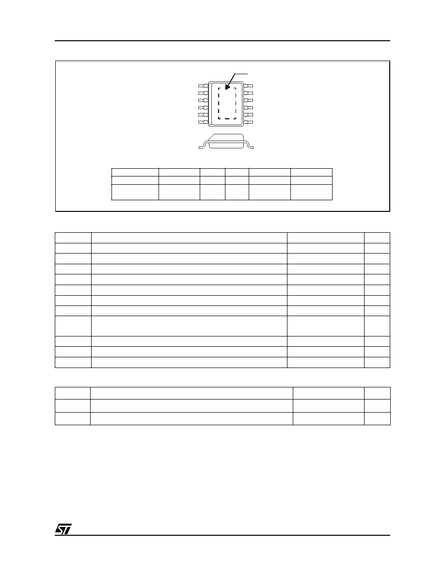
Figure 1. Package
This device integrates an analog current sense
which delivers a current proportional to the load
current (according to a known ratio) when CS_DIS
is driven low or left open.
When CS_DIS is driven high, the CURRENT
SENSE pin is in a high impedance condition.
Output current limitation protects the device in
overload condition. In case of long overload
duration, the device limits the dissipated power to
safe level up to thermal shut-down intervention.
Thermal shut-down with automatic restart allows
the device to recover normal operation as soon as
fault condition disappears.
Table 2. Order Codes
Note: (*) See application schematic at page 8
TYPE
V
CC
R
DS(on)
I
D
VN5016AJ-E
41V
16m
40A
PowerSSO-12
Package
Tube
Tape and Reel
PowerSSO-12
VN5016AJ-E
VN5016AJTR-E
ADVANCE DATA

VN5016AJ-E
2/13
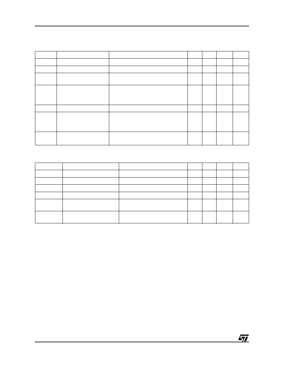
Figure 2. Block Diagram
Table 3. Pin Function
Figure 3. Current and Voltage Conventions
Name
Function
V
CC
Battery connection
OUTPUT
Power output
GND
Ground connection. Must be reverse battery protected by an external diode/resistor network
INPUT
Voltage controlled input pin with hysteresis, CMOS compatible. Controls output switch state
CURRENT SENSE
Analog current sense pin, delivers a current proportional to the load current
CS_DIS
Active high CMOS compatible pin, to disable the current sense pin
LOGIC
UNDERVOLTAGE
OVERTEMP.
I
LIM
PwCLAMP
K
I
OUT
GND
INPUT
V
CC
OUTPUT
CURRENT
SENSE
DRIVER
V
CC
CLAMP
V
DSLIM
CS_DIS
Pwr
LIM
I
S
I
GND
V
CC
V
CC
V
SENSE
OUTPUT
I
OUT
CURRENT SENSE
I
SENSE
INPUT
I
IN
V
IN
V
OUT
GND
CS_DIS
I
CSD
V
CSD
V
F
3/13
VN5016AJ-E
Figure 4. Configuration Diagram (Top View) & Suggested Connections For Unused and n.c. Pins
Table 4. Absolute Maximum Ratings
Table 5. Thermal Data
Note: 1. When mounted on a standard single-sided FR4 board with 0.5cm
2
of Cu (at least 35 µm thick) connected to TAB.
Symbol
Parameter
Value
Unit
V
CC
DC supply voltage
41
V
-V
CC
Reverse DC supply voltage
-0.3
V
- I
GND
DC reverse ground pin current
-200
mA
I
OUT
DC output current
Internally limited
A
- I
OUT
Reverse DC output current
-30
A
I
IN
DC input current
-1 to 10
mA
I
CSD
DC current sense disable input current
-1 to 10
mA
V
CSENSE
Current sense maximum voltage
V
CC
-41
+V
CC
V
V
V
ESD
Electrostatic discharge (R=1.5k
; C=100pF)
2000
V
T
j
Junction operating temperature
-40 to 150
°C
T
stg
Storage temperature
-55 to 150
°C
Symbol
Parameter
Max Value
Unit
R
thj-case
Thermal resistance junction-case
2.3
°C/W
R
thj-amb
Thermal resistance junction-ambient
75 (see note 1)
°C/W
Connection / Pin Current Sense
N.C.
Output
Input
CS_DIS
Floating
X
X
X
X
To Ground
Through 1K
resistor
X
Through 10K
resistor
Through 10K
resistor
TAB = V
cc
OUTPUT
OUTPUT
OUTPUT
OUTPUT
OUTPUT
OUTPUT
12
11
10
9
8
7
1
2
3
4
5
6
V
CC
V
CC
INPUT
CURRENT SENSE
GND
CS_DIS
VN5016AJ-E
4/13
ELECTRICAL CHARACTERISTICS (8V<V
CC
<36V; -40
°C
<T
j
<150
°C
, unless otherwise specified)
Table 6. Power Section
Note: (**) PowerMOS leakage included
Table 7. Switching (V
CC
=13V)
Symbol
Parameter
Test Conditions
Min.
Typ.
Max.
Unit
V
CC
Operating supply voltage
4.5
13
36
V
V
USD
Undervoltage shutdown
3
4.5
V
V
USDhyst
Undervoltage Shut-down
hysteresis
0.5
V
R
ON
On state resistance
I
OUT
=5A; T
j
=25°C
I
OUT
=5A; T
j
=150°C
I
OUT
=5A; V
CC
=5V; T
j
=25°C
16
32
20
m
m
m
V
clamp
Clamp Voltage
I
S
=20mA
41
46
52
V
I
S
Supply current
Off State; V
CC
=13V; T
j
=25°C;
V
IN
=V
OUT
=V
SENSE
=V
CSD
=0V
On State; V
CC
=13V; V
IN
=5V; I
OUT
=0A
2(**)
1.5
5(**)
3
µ
A
mA
I
L(off)
Off state output current
V
IN
=V
OUT
=0V; V
CC
=13V; T
j
=25°C
V
IN
=V
OUT
=0V; V
CC
=13V; T
j
=125°C
0
0
3
5
µ
A
Symbol
Parameter
Test Conditions
Min.
Typ.
Max.
Unit
t
d(on)
Turn-on delay time
R
L
=2.6
15
µ
s
t
d(off)
Turn-off delay time
R
L
=2.6
40
µ
s
(dV
OUT
/dt)
on
Turn-on voltage slope
R
L
=2.6
0.3
V
/µ
s
(dV
OUT
/dt)
off
Turn-off voltage slope
R
L
=2.6
0.35
V
/µ
s
W
ON
Switching losses energy at
turn-on
R
L
=2.6
TBD
mJ
W
OFF
Switching losses energy at
turn-off
R
L
=2.6
TBD
mJ

5/13
VN5016AJ-E
ELECTRICAL CHARACTERISTICS (continued)
Table 8. Logic Input
Table 9. Protections and Diagnostics (see note 2)
Note: 2. To ensure long term reliability under heavy overload or short circuit conditions, protection and related diagnostic signals must be
used together with a proper software strategy. If the device is subjected to abnormal conditions, this software must limit the duration
and number of activation cycles
Symbol
Parameter
Test Conditions
Min.
Typ.
Max.
Unit
V
IL
Input low level voltage
0.9
V
I
IL
Low level input current
V
IN
=0.9V
1
µ
A
V
IH
Input high level voltage
2.1
V
I
IH
High level input current
V
IN
=2.1V
10
µ
A
V
I(hyst)
Input hysteresis voltage
0.25
V
V
ICL
Input clamp voltage
I
IN
=1mA
I
IN
=-1mA
5.5
-0.7
TBD
V
V
V
CSDL
CS_DIS low level voltage
0.9
V
I
CSDL
Low level CS_DIS current
V
CSD
=0.9V
1
µ
A
V
CSDH
CS_DIS high level voltage
2.1
V
I
CSDH
High level CS_DIS current
V
CSD
=2.1V
10
µ
A
V
CSD(hyst)
CS_DIS hysteresis voltage
0.25
V
V
CSCL
CS_DIS clamp voltage
I
CSD
=1mA
I
CSD
=-1mA
5.5
-0.7
TBD
V
V
Symbol
Parameter
Test Conditions
Min.
Typ.
Max.
Unit
I
limH
DC Short circuit current
V
CC
=13V
5V<V
CC
<36V
40
60
80
80
A
A
I
limL
Short circuit current
during thermal cycling
V
CC
=13V T
R
<T
j
<T
TSD
24
A
T
TSD
Shutdown temperature
150
175
200
°C
T
R
Reset temperature
T
RS
+ 1
T
RS
+ 5
°C
T
RS
Thermal reset of STATUS
135
°C
T
HYST
Thermal hysteresis
(T
TSD
-T
R
)
7
°C
V
DEMAG
Turn-off output voltage
clamp
I
OUT
=2A; V
IN
=0; L=6mH
V
CC
-41
V
CC
-46 V
CC
-52
V
V
ON
Output voltage drop
limitation
I
OUT
=0.3A; T
j
= -40°C...+150°C
(see figure 9)
25
mV